
Design and Optimization of High-Responsivity High-Speed Ge/Si Avalanche Photodiode in the C+L Band

1
State Key Laboratory of Functional Materials for Informatics, Shanghai Institute of Microsystem and Information Technology, Chinese Academy of Sciences, Shanghai 200050, China
2
University of Chinese Academy of Sciences, Beijing 100049, China
3
Shanghai Industrial Technology Research Institute, Shanghai 201800, China
*
Authors to whom correspondence should be addressed.
Micromachines 2023, 14(1), 108; https://doi.org/10.3390/mi14010108
Submission received: 15 December 2022
/
Revised: 27 December 2022
/
Accepted: 28 December 2022
/
Published: 30 December 2022
(This article belongs to the Special Issue Silicon Photonic Devices and Integration)
Abstract
:We present the design of Ge/Si avalanche photodetectors with SiN stressor-induced Ge strain for the C+L band light detection. By optimizing the placement position and thickness of the SiN layer with compressive stress, a uniform strain distribution with a maximum magnitude of 0.59% was achieved in Ge. The surface-illuminated APDs have been studied in respect of the photo-dark current, responsivity, gain, and 3-dB bandwidth. After introducing SiN stressor, the APD exhibits high primary responsivity of 0.80 A/W at 1.55 μm, 0.72 A/W at 1.625 μm, and 3-dB bandwidth of 17.5 GHz. The increased tensile strain in Ge can significantly improve the responsivity and broaden the response band of the device. This work provides a constructive approach to realizing high-responsivity high-speed Ge/Si APD working in the C+L band.
1. Introduction
In view of the high optical absorption of germanium in the near-infrared band, the research on germanium/silicon avalanche photodiodes (APDs) mostly focuses on the wavelength of 1.31 μm [1,2,3]. The Intel team first proposed a separate-absorption-charge-multiplication (SACM) APD structure and achieved a primary responsivity of 0.55 A/W at 1.31 μm and high gain-bandwidth product of 340 GHz, which was equivalent to commercial III-V compound APDs [4]. Nevertheless, applications like sensing, laser radar, and medical diagnostics require APDs with higher responsivity and wider detection bands [5,6]. Limited by the energy band structure of Ge, its absorption coefficient starts to drop sharply from 1.55 μm, resulting in the low responsivity of traditional Ge/Si APDs in the C+L band. To enhance light absorption, surface-illuminated APDs usually adopt thick absorption layers. However, this also leads to an increased carrier transit time and reduced 3-dB bandwidth. The vertical surface-illuminated SACM-APD proposed by the IME achieved a primary responsivity of 0.3 A/W and a 3 dB bandwidth of 13 GHz at 1.55 μm with a 1 μm thick Ge layer [7]. Therefore, how to realize high-speed and high-responsivity surface-illuminated APD in the C+L band is an urgent issue to be addressed.
A diverse range of measures, including on-silicon lead-free halide perovskite single-crystalline thin film (SCTF), nanostalagmite structures, Ge nanowires, grating structures, graphene interlayer, reflector mirror, and tensile strain, have been investigated to enable high-performance photodetectors [8,9,10,11,12,13,14]. Of them, tensile strain is considered an effective measure to enhance the optical properties of Ge [15]. Several methods have been proposed for introducing the strain in Ge, such as thermally induced strain during epitaxial growth on Si, the use of a stressor layer, etc. [16]. Among these, the application of silicon nitride as a stressor layer has been widely studied, mainly because of its compatibility with CMOS processes and flexible control of stress transfer to attain high tensile strain in Ge [17]. Moustafa El Kurdi et al. used an omnidirectional SiN stressor to coat Ge microdisk, achieved a biaxial tensile strain of 1.75%, and transformed Ge into a direct bandgap semiconductor [18]. Besides, Lin Y et al. employed a recessed SiN stressor to elevate the tensile strain of Ge to 0.56% in germanium-on-insulator (GOI) metal-semiconductor-metal photodiodes, with an extra 10~60% rise in the absorption coefficient of C+L band [19].
In this paper, a high-performance surface-illuminated SACM Ge/Si APD was designed. The SiN stressor layer was used to introduce tensile strain into Ge to strengthen its absorption coefficient in the C+L band. The influence of the SiN stressor on the in-plane strain εxx distribution in Ge was explored and uniformly distributed εxx of 0.59% amplitude was obtained. Furthermore, the device structure was optimized considering the constraint relationship between the responsivity and bandwidth. The optimal structure of this design improved the primary responsivity of 0.80 A/W at 1.55 μm, 0.72 A/W at 1.625 μm with a high speed of 17.5 GHz 3-dB bandwidth.
2. Design of Si-Based Strained Ge APD
Under the theory of deformation potential [20], the introduction of tensile strain will cause the reduction of Γ and L valleys in the conduction band and the separation of light- and heavy-hole valence bands of Ge, attaining lower direct and indirect bandgaps of Ge which can be described as quadratic polynomials of the strain [21]:
, are the bandgaps of each valley to the light hole and heavy hole, is the bandgap of bulk Ge. Where , , indicate the in-plane strain and the strain perpendicular to the film, respectively, with the relationship . and are the deformation potential constants of Ge, is the spin-orbit separation energy. The direct bandgap absorption coefficient of strained Ge can be expressed as:
where is a constant related to the effective mass of the materials. As the bandgap of strained Ge shrinks, the absorption coefficient in its response band increases as well as the response wavelength extends to the L-band [22].
Since the different thermal expansion coefficients of Ge/Si, the Ge-on-Si epitaxial growth and cooling resulted in an inherent tensile strain of 0.15~0.3% in Ge [23,24], it was assumed that an initial even strain is 0.25% [25]. The location of the SiN stressor will affect the magnitude and uniformity of the introduced strain in Ge. Multi-physics simulation is used to investigate the x-directional strain εxx distribution in Ge transferred from SiN stressor under different device structures. Owing to the centrosymmetric nature of the surface-illuminated APD, εxx can be expressed as an in-plane strain. The diameter of the mesa structure on the N+ electrode is 5 µm, the pre-stress in SiN is set to be 3 GPa. It can be observed that only the upper surface of Ge is subjected to the stress transmitted by SiN stressor in Figure 1a,c. The distribution of εxx in Ge is less uniform. However, because of the addition of SiN stressor on the sides of the mesa and the lower steps, both the left and right Ge are subjected to the stress transfer as well, the evenness of εxx in Ge in Figure 1b,d was significantly enhanced. Furthermore, it can be found that by replacing the SiO2 layer in the SOI substrate with SiN stressor, the overall tensile strain in Ge is raised. The maximum value of εxx has been increased from 0.28% to 0.34%. At the same time, Ge is affected by stress transfer from all directions, the strain homogeneity is remarkably improved. Structure 4 has achieved an evenly distributed εxx with an amplitude of 0.34%, which is the most optimal structure. The following will analyze several factors affecting the tensile strain in Ge based on structure 4.
In structure 4, the thickness of the upper and lower SiN stressors will influence the strain distribution in Ge. When the thickness of the upper and lower SiN layers is both 0.6 µm and the sidewall SiN is 0.3 µm, the profile of εxx in Ge is exhibited in Figure 1d. The strain values of εxx in regions 1–4 are 0.329%, 0.331%, 0.270%, and 0.248%, respectively, which revealed a high degree of homogeneity. Moreover, these values increase synchronously with the thickness of the upper SiN stressor (Figure 2a). When the thickness of top SiN layer is only 0.2 µm, the values of εxx in regions 1–4 are 0.217%, 0.227%, 0.213%, and 0.225%, respectively. While as the SiN thickness reaches 0.8 µm, the strain then rises to 0.355%, 0.341%, 0.279%, 0.251%, and the speed of increasing gradually slows down. In addition, the strain at the bottom part of Ge (region 3 and 4) elevates rapidly as the thickness of the underlying SiN layer is added, exhibiting a ~1.75x enhancement (Figure 2b). When the thickness of lower SiN is 0.2 µm, the values of εxx in regions 1–4 are 0.279%, 0.282%, 0.193%, 0.163%, and then increase to 0.347%, 0.348%, 0.301%, 0.279% when the thickness becomes 0.8 µm. The uniformity of the strain distribution is also improved. The thicker the SiN stressor is, the higher the overall strain εxx in Ge. Nevertheless, excessively thick SiN stressor deposition will lead to larger wafer warpage, which is not conducive for process integration. 0.6 µm thickness of the upper and lower SiN layers are selected to obtain up to 0.34% in-plane tensile strain in Ge.
Figure 3 simulates the in-plane strain εxx in Ge for structure 4 with different mesa diameters under the same SiN stressor setting. In the previous study, the εxx in Ge was uniformly distributed and reached 0.329% in region 1, the strain in the edge area was slightly higher at 0.34%. It can be seen that when the mesa diameter is 10 µm (Figure 3a), the maximum strain in Ge keeps shifting toward the edge region and the amplitude drops to 0.26%. The strain in the central region of Ge continuously diminishes to the range of 0.05~0.1%, only about 0.23% strain exists in the edge region, upon the diameter of the mesa increases to 20 µm (Figure 3b). Furthermore, when the mesa diameter is 30 µm, the low strain region in the middle of Ge expands and remains the range of 0~0.05%, the edge region still maintains a strain of about 0.23% (Figure 3c). It can also be seen from the curves of the variation of εxx in region 1 and 2 with mesa diameter in Figure 3d, the larger the size of Ge, the more dispersion of the SiN stress transfer and the lower the overall strain, which is detrimental to the optimization of Ge light absorption.
Based on the above analysis, both structures 2 and 4 achieve a relatively uniform strain distribution in Ge. The strain amplitude in Ge of structure 2 can reach 0.53%, while structure 4 has the most homogeneous strain distribution and a maximum magnitude of 0.59%, which is the optimal strain level. Figure 4 presents the three-dimensional structure as well as the doping and thickness of each layer for the SACM APD based on structure 2. Due to the excellent chemical stability of SiN, it can be used as a device surface protection film. SiN also features good optical properties with a refractive index of around 2.0. The SiN on the photosensitive surface can be applied as an anti-reflective coating (ARC) layer to reduce the reflection of incident light utilizing the thin film interference principle. Since aluminum can attain over 85% reflectivity for the light range of 0.4~10 μm [26], a 0.1 μm thick aluminum layer was added to the back of the device as a reflective layer [27]. Under the effect of the resonant cavity formed by the top ARC layer and the bottom reflective layer, the incident light was reflected in it to generate resonance enhancement (RCE) with the goal of raising the responsivity of the device [28].
3. Results and Discussion
3.1. IV Characteristics
Although structure 4 is better than structure 2 in terms of homogeneity and strain amplitude, achieving the optimal strain level, structure 2 is more manufacturable in practical fabrication. Consequently, the device performance simulations employing technology computer-aided design (TCAD) software will be carried out for the surface-illuminated APDs with structures 2 and 4.
Figure 5a shows the curves of the photocurrent density as a function of applied reverse bias voltage for the four types of APDs in Table 1. According to Figure 5b, the dark current reaches 10−4 A at −20.2 V, which can be defined as the avalanche multiplication voltage Vbr. The photocurrent density is achieved at a normal incidence of 2 W/cm2 light intensity at 1.55 μm wavelength. At 0.95Vbr, the photocurrent density of type 1 is only 1.07 × 10⁻⁶ A/μm, the corresponding device optical absorption is 45.1%. When the resonant cavity is added to form RCE, the photocurrent density of type 2 reaches 1.35 × 10⁻⁶ A/μm, the optical absorption increases significantly to 62.3%. The tensile strain amplitude in Ge of type 3 is up to 0.53% as well as the photocurrent density and absorption rate reach 1.45 × 10⁻⁶ A/μm and 67.2%, separately. Because type 4 employs the optimal strain simulation structure, the strain in Ge is as high as 0.59% with 1.47 × 10⁻⁶ A/μm photocurrent density and 68.2% light absorption. The introduction of the RCE structure together with the SiN stressor notably enhances the light absorption of the device. The gap between type 3 and type 4 in terms of photocurrent and device optical absorption is inconspicuous.
Analyzing the rectification behavior of the device for dark current density variation displayed in Figure 5b. When the bias voltage Vbias is above −5 V, the depletion region exists only in Si at a relatively low dark current. As the Vbias increases, the depletion region expands into Ge, leading to a rise in dark current due to the generation-recombination current in the absorption region [29]. The punch-through of Ge occurs between −12 and −5 V, and the capacitance characteristics of APD also confirm that Ge is completely depleted at −12 V with the minimum value of 2.82fF.
3.2. Responsivity Characteristics
The primary responsivity (gain = 1) Rp can be obtained by responsivity testing of p-i-i-n device without a charge layer. The Rp of the four types of APDs in the incident light wavelength range of 1.3~1.66 μm is illustrated in Figure 6a. For type 1, considering only the initial strain in Ge, its Rp at 1.55 μm is only 0.54 A/W. Type 2 demonstrates a high Rp of 0.71 A/W at 1.55 μm after the addition of the RCE. By contrast, type 3 extends the response band to L band upon the adoption of SiN stressor, where the Rp rises to 0.78 A/W at 1.55 μm and 0.64 A/W at 1.625 μm. As the improved strain uniformity and amplitude in Ge of type 4, the Rp is overall higher than that of type 3, especially in the L-band, reaching 0.80 A/W at 1.55 μm and 0.72 A/W at 1.625 μm.
The SiN served as the top mirror in the RCE structure is not as thick as possible. As shown in Figure 6b, it can be found that when the thickness of upper SiN is 0.6 μm, the Rp of type 3 and type 4 are maximized at 1.55 and 1.625 μm, and the highest light absorption rate of type 3, 4 reach 67.3%, 68.3% at 1.55 μm and 54.7%, 59.7% at 1.625 μm, respectively. Hence, the optimal thickness of SiN as the upper surface ARC layer is 0.6 μm, which is consistent with the size used in the strain simulation.
The responsivity and gain at 1.55 and 1.625 μm wavelength incident light of 2 W/cm2 light intensity as a function of Vbias is further investigated for type 4 device (Figure 6c). At 0.95Vbr, the responsivity along with the gain at 1.55 μm is 14.7 A/W and 18.4, while those at 1.625 μm are 13.5 A/W and 18.8.
3.3. Trade-Off between Responsivity and Bandwidth
Since the photon propagation path of the surface-illuminated APD is in the same direction as the carrier multiplication path, there is a restrictive relationship between the responsivity and bandwidth [30]. Then three groups of different Ge absorption layer thicknesses (0.6 μm, 0.7 μm, 0.8 μm) were chosen for type 3 and type 4 to simulate the Rp and 3-dB bandwidth f3-dB, select the appropriate thickness to attain high-performance device.
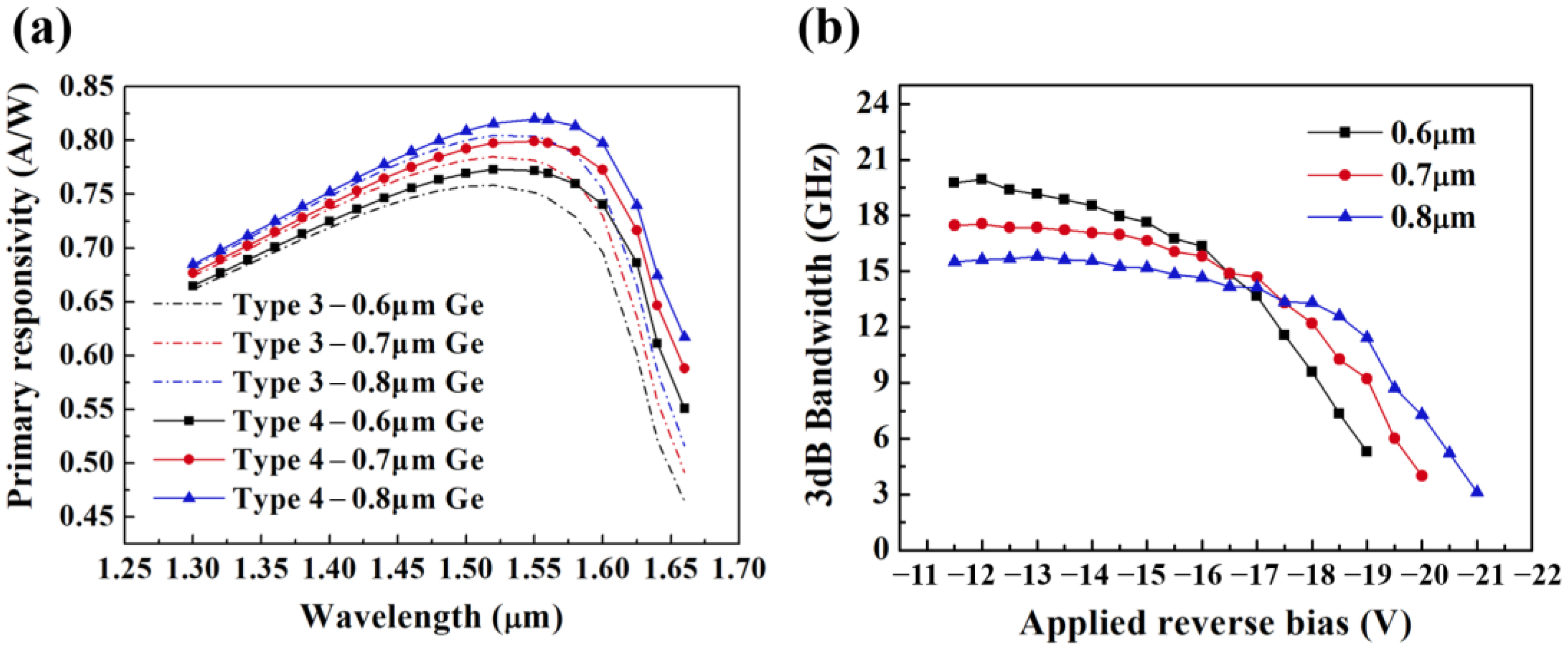
Figure 7a presents the changing curves of Rp in the 1.3~1.7 μm band for APDs with different absorption layer thicknesses. As the Ge thickness grows, the length of the absorption region grows and the Rp goes up. The Rp of type 3 and type 4 at 1.55 μm increases from 0.75, 0.77 A/W to 0.80, 0.82 A/W, and the Rp at 1.625 μm rises from 0.60, 0.69 A/W to 0.67, 0.74 A/W along with the thickness goes up from 0.6 to 0.8 μm. Figure 7b illustrates the variation of the f3-dB values as a function of Vbias for different Ge thickness. Since type 3 and type 4 utilize the same SACM structure, the f3-dB values are almost identical. As the thickness of Ge absorption layer increases from 0.6 um to 0.8 um, the carrier transit time rises with the f3-dB at low gain and decreases from 19.8 to 15.5 GHz continuously. Rp and f3-dB values of the surface-illuminated APD vary in opposite trends with absorption layer thickness. Hence, a Ge absorption layer with 0.7 μm thickness is chosen as a compromise to realize high-responsivity and high-speed Ge/Si APD.
Table 2 summarizes the reported experimental performance parameters of Ge/Si APDs. As the waveguide-integrated APDs can elongate the length of the absorption region to capture high responsivity without affecting the response speed. The waveguide APD using thin silicon achieved 25 GHz f3-dB and 0.75 A/W at 1.55 μm [31]. However, the operating voltage gain value inversely proportional to the thickness of the multiplication zone is 12, lower than the conventional surface incidence APDs. Moreover, this structure is not as capable of collecting scattered light signals in the domain of freely spatial communication as the surface incidence structure [32]. The surface-illuminated APD designed from this work exhibits a high bandwidth simulation value of 17.5 GHz through reduction of the multiplication region, which is better than the reported surface incident APDs and comparable to the waveguide types. The gain value at 0.95Vbr thus drops to 18 with a gain-bandwidth product (GBP) of 162 GHz. Besides, the Rp of this design achieves 0.8 A/W at 1.55 μm, which is superior to the reported results in Table 2 and second only to the 0.9 A/W of the APD with the optimized RCE structure by SiFotonics, whose responsivity plummeted in the L band [28]. In stark contrast, the present APD attains an Rp of 0.72 A/W at 1.625 μm. In summary, there are advantages of Ge/Si surface-illuminated APD with SiN stressor in both responsivity and bandwidth according to the simulation results. Moreover, the effect of RCE structure on the responsivity is also very considerable, and the design of the resonant cavity can be carefully optimized subsequently to further enhance the device’s performance.
4. Conclusions
A high-performance surface-illuminated Ge/Si APD applied to C+L band light detection is designed using SiN stressor to improve the optical properties of Ge. Two structures with a homogeneous distribution of tensile strain in Ge and magnitude up to 0.53% and 0.59%, respectively, are proposed. The adoption of the resonant cavity substantially boots the light absorption in the response band of APD, and the elevation of tensile strain in Ge slightly raises the responsivity of the device in the C-band, simultaneously extending the detection band to the L-band. For the optimized design of Ge/Si APD with 0.59% amplitude tensile strain in Ge captures an Rp of 0.80 A/W at 1.55 μm and 0.72 A/W at 1.625 μm, the f3-dB at a low gain is maintained at 17.5 GHz. This work demonstrates that mechanical strain engineering is a promising scheme to achieve high-speed, high-responsivity Ge/Si APDs in the C+L band.
Author Contributions
Data curation, C.L.; formal analysis, C.L.; investigation, C.L.; methodology, C.L. and X.L.; software, C.L. and X.L.; supervision, W.W. and Y.C.; visualization, C.L.; writing—original draft preparation, C.L.; writing—review and editing, W.W., Y.C. and M.Y. All authors have read and agreed to the published version of the manuscript.
Funding
This research was funded by the National Key R&D Program of China (2021YFB0301000); and Strategic Pioneer Research Projects of Defense Science and Technology (XDB43020500).
Data Availability Statement
Not applicable.
Conflicts of Interest
The authors declare no conflict of interest.
References
- Xiang, Y.; Cao, H.; Liu, C.; Dai, D. High-performance waveguide Ge/Si avalanche photodiode with a lateral separate-absorption-charge-multiplication structure. Opt. Express 2022, 30, 11288–11297. [Google Scholar] [CrossRef]
- Park, S.; Malinge, Y.; Dosunmu, O.; Lovell, G.; Slavin, S.; Magruder, K.; Kang, Y.; Liu, A. 50-Gbps Receiver Subsystem Using Ge/Si Avalanche Photodiode and Integrated Bypass Capacitor. In Proceedings of the 2019 Optical Fiber Communications Conference and Exposition (OFC), San Diego, CA, USA, 3–7 March 2019; p. M3A.3. [Google Scholar]
- Huang, M.; Cai, P.; Li, S.; Hou, G.; Zhang, N.; Su, T.-I.; Hong, C.; Pan, D. 56GHz waveguide Ge/Si avalanche photodiode. In Proceedings of the 2018 Optical Fiber Communications Conference and Exposition (OFC), San Diego, CA, USA, 11–15 March 2018; p. W4D.6. [Google Scholar]
- Kang, Y.; Liu, H.D.; Morse, M.; Paniccia, M.J.; Zadka, M.; Litski, S.; Sarid, G.; Pauchard, A.; Kuo, Y.H.; Chen, H.W.; et al. Monolithic germanium/silicon avalanche photodiodes with 340 GHz gain–bandwidth product. Nat. Photonics 2009, 3, 59–63. [Google Scholar] [CrossRef]
- Ng, J.S.; Tan, C.H.; Davide, J.P.R. Avalanche Photodiodes beyond 1.65μm. Proc. of SPIE 2009, 7320, 73200V1–73200V11. [Google Scholar]
- Dong, Y.; Wang, W.; Xu, X.; Gong, X.; Lei, D.; Zhou, Q.; Xu, Z.; Loke, W.K.; Yoon, S.F.; Liang, G.; et al. Germanium-Tin on Si avalanche photodiode: Device design and technology demonstration. IEEE Trans. Electron Devices 2015, 62, 128–135. [Google Scholar] [CrossRef]
- Duan, N.; Liow, T.Y.; Lim, A.E.-J.; Ding, L.; Lo, G.Q. 310 GHz gain-bandwidth product Ge/Si avalanche photodetector for 1550 nm light detection. Opt. Express 2012, 20, 11031–11036. [Google Scholar] [CrossRef] [PubMed]
- Li, Z.; Liu, X.; Zuo, C.; Yang, W.; Fang, X. Supersaturation-Controlled Growth of Monolithically Integrated Lead-Free Halide Perovskite Single-Crystalline Thin Film for High-Sensitivity Photodetectors. Adv. Mater. 2021, 31, 2103010. [Google Scholar] [CrossRef]
- Zhang, Y.; Loh, J.Y.Y.; Kherani, N.P. Facilely Achieved Self-Biased Black Silicon Heterojunction Photodiode with Broadband Quantum Efficiency Approaching 100%. Adv. Mater. 2022, 9, 2203234. [Google Scholar] [CrossRef]
- Gao, F.; Wang, J.H.; Watzinger, H.; Hu, H.; Rancic, M.J.; Zhang, J.Y.; Wang, T.; Yao, Y.; Wang, G.L.; Kukucka, J.; et al. Site-Controlled Uniform Ge/Si Hut Wires with Electrically Tunable Spin-Orbit Coupling. Adv. Mater. 2020, 32, 1906523. [Google Scholar] [CrossRef] [PubMed] [Green Version]
- Zhu, X.; Choy, W.C.H.; Xie, F.; Duan, C.; Wang, C.; He, W.; Huang, F.; Cao, Y. A study of optical properties enhancement in low-bandgap polymer solar cells with embedded PEDOT:PSS gratings. Sol. Energy Mater. Sol. Cells 2012, 99, 327–332. [Google Scholar] [CrossRef]
- Lin, L.; Ou, Y.; Zhu, X.; Stamate, E.; Wu, K.; Liang, M.; Liu, Z.; Yi, X.; Herstrom, B.; Boisen, A.; et al. InGaN/GaN ultraviolet LED with a graphene/AZO transparent current spreading layer. Opt. Mater. Express 2018, 8, 1818–1826. [Google Scholar] [CrossRef] [Green Version]
- Yuan, Y.; Huang, Z.; Zeng, X.; Liang, D.; Sorin, W.V.; Fiorentino, M.; Beausoleil, R.G. High Responsivity Si-Ge Waveguide Avalanche Photodiodes Enhanced by Loop Reflector. IEEE J. Sel. Top. Quantum Electron 2021, 28, 1–8. [Google Scholar] [CrossRef]
- Tani, K.; Oda, K.; Okumura, T.; Takezaki, T.; Kasai, J.-i.; Mine, T.; Ido, T. Enhanced Electroluminescence from Germanium Waveguides by Local Tensile Strain with Silicon Nitride Stressors. In Proceedings of the 2013 International Conference on Solid State Devices and Materials (SSDM), Fukuoka, Japan, 23–27 September 2013; pp. 1032–1033. [Google Scholar]
- Saito, S.; Gardes, F.Y.; Al-Attili, A.Z.; Tani, K.; Oda, K.; Suwa, Y.; Ido, T.; Ishikawa, Y.; Kako, S.; Iwamoto, S.; et al. Group IV Light Sources to Enable the Convergence of Photonics and Electronics. Front. Mater. 2014, 1, 1–15. [Google Scholar] [CrossRef] [Green Version]
- Xiong, W.; Wang, G.; Li, J.; Zhao, C.; Wang, W.; Radamson, H.H. SiN-based platform toward monolithic integration in photonics and electronics. J Mater Sci: Mater. Electron. 2021, 32, 1–18. [Google Scholar] [CrossRef]
- Millar, R.W.; Gallacher, K.; Frigerio, J.; Ballabio, A.; Bashir, A.; MacLaren, I.; Isella, G.; Paul, D.J. Analysis of Ge micro-cavities with in-plane tensile strains above 2%. Opt. Express 2016, 24, 4365–4374. [Google Scholar] [CrossRef] [Green Version]
- Kurdi, M.E.; Prost, M.; Ghrib, A.; Sauvage, S.; Checoury, X.; Beaudoin, G.; Sagnes, I.; Picardi, G.; Ossikovski, R.; Boucaud, P. Direct Band Gap Germanium Microdisks Obtained with Silicon Nitride Stressor Layers. ACS Photonics 2016, 3, 443–448. [Google Scholar] [CrossRef]
- Lin, Y.; Ma, D.; Lee, K.H.; Wen, R.T.; Syaranamual, G.; Kimerling, L.C.; Tan, C.S.; Michel, J. PIC-integrable, uniformly tensile-strained Ge-on-insulator photodiodes enabled by recessed SiNx stressor. Photonics Res. 2021, 9, 1255–1263. [Google Scholar] [CrossRef]
- Van de Walle, C.G. Band lineups and deformation potentials in the model-solid theory. Phys. Rev. B. 1989, 39, 1871–1883. [Google Scholar]
- Liu, J.; Cannon, D.D.; Wada, K.; Ishikawa, Y.; Danielson, D.T.; Jongthammanurak, S.; Michel, J.; Kimerling, L.C. Deformation potential constants of biaxially tensile stressed Ge epitaxial films on Si (100). Phys. Rev. B. 2004, 70, 155309. [Google Scholar] [CrossRef]
- Liu, J.; Sun, X.; Pan, D.; Wang, X.; Kimerling, L.C.; Koch, T.L.; Michel, J. Tensile-strained, n-type Ge as a gain medium for monolithic laser integration on Si. Opt. Express 2007, 15, 11272–11277. [Google Scholar] [CrossRef]
- Yurasov, D.V.; Bobrov, A.I.; Daniltsev, V.M.; Novikov, A.V.; Pavlov, D.A.; Skorokhodov, E.V.; Shaleev, M.V.; Yunin, P.A. Impact of growth and annealing conditions on the parameters of Ge/Si (001) relaxed layers grown by molecular beam epitaxy. Semiconductors 2015, 49, 1415–1420. [Google Scholar] [CrossRef]
- Capellini, G.; Seta, M.D.; Zaumseil, P.; Kozlowski, G.; Schroeder, T. High temperature x ray diffraction measurements on Ge/Si (001) heterostructures: A study on the residual tensile strain. J. Appl. Phys. 2012, 111, 073518. [Google Scholar] [CrossRef]
- Novikov, A.V.; Yurasov, D.V.; Morozova, E.E.; Skorohodov, E.V.; Verbus, V.A.; Yablonskiy, A.N.; Baidakova, N.A.; Gusev, N.S.; Kudryavtsev, K.E.; Nezhdanov, A.V.; et al. Formation and Properties of Locally Tensile Strained Ge Microstructures for Silicon Photonics. Semiconductors 2018, 52, 1442–1447. [Google Scholar] [CrossRef]
- Cheng, B.W.; Li, C.B.; Yao, F.; Xue, C.L.; Zhang, J.G.; Mao, R.W.; Zuo, Y.H.; Luo, L.P.; Wang, Q.M. Silicon membrane resonant-cavity-enhanced photodetector. Appl. Phys. Lett. 2005, 87, 061111. [Google Scholar] [CrossRef]
- Li, G.; André, N.; Poncelet, O.; Gérard, P.; Ali, S.Z.; Udrea, F.; Francis, L.A.; Zeng, Y.; Flandre, D. Operation of Suspended Lateral SOI PIN Photodiode with Aluminum Back Gate. In Proceedings of the 2016 Joint International EUROSOI Workshop and International Conference on Ultimate Integration on Silicon (EUROSOI-ULIS), Vienna, Austria, 25–27 January 2016; pp. 155–158. [Google Scholar]
- Huang, M.; Li, S.; Cai, P.; Hou, G.; Su, T.I.; Chen, W.; Hong, C.Y.; Pan, D. Germanium on Silicon Avalanche Photodiode. IEEE J. Sel. Top. Quantum Electron 2018, 24, 1–11. [Google Scholar] [CrossRef]
- Kang, Y.; Zadka, M.; Litski, S.; Sarid, G.; Morse, M.; Paniccia, M.J.; Kuo, Y.H.; Bowers, J.; Beling, A.; Liu, H.D.; et al. Epitaxially-grown Ge/Si avalanche photodiodes for 1.3μm light detection. Opt. Express 2008, 16, 9365–9371. [Google Scholar] [CrossRef] [PubMed]
- Wang, B.; Mu, J. High-speed Si-Ge avalanche photodiodes. PhotoniX 2022, 3, 1–22. [Google Scholar] [CrossRef]
- Huang, Z.; Li, C.; Liang, D.; Yu, K.; Santori, C.; Fiorentino, M.; Sorin, W.; Palermo, S.; Beausoleil, R.G. A 25Gbps low-voltage waveguide Si-Ge avalanche photodiode. Optica 2016, 3, 793–798. [Google Scholar] [CrossRef]
- Liu, X.; Li, X.; Li, Y.; Li, Y.; Zhi, Z.; Tao, M.; Chen, B.; Zhang, L.; Guo, P.; Lo, G.; et al. Three-terminal germanium-on-silicon avalanche photodiode with extend p-charge layer for dark current reduction. Photonics Res. 2022, 10, 1956–1963. [Google Scholar] [CrossRef]
- Srinivasan, S.A.; Berciano, M.; Heyn, P.D.; Lardenois, S.; Pantouvaki, M.; Campenhout, J.V. 27 GHz Silicon-Contacted Waveguide-Coupled Ge/Si Avalanche Photodiode. J. Lightwave Technol. 2020, 38, 3044–3050. [Google Scholar] [CrossRef]
- Benedikovic, D.; Virot, L.; Aubin, G.; Hartmann, J.M.; Amar, F.; Roux, X.L.; Alonso-Ramos, C.; Cassan, E.; Marris-Morini, D.; Crozat, P.; et al. 40 Gbps heterostructure germanium avalanche photo receiver on a silicon chip. Optica 2020, 7, 775–783. [Google Scholar] [CrossRef]
- Zeng, X.; Huang, Z.; Wang, B.; Liang, D.; Fiorentino, M.; Beausoleil, R.G. Silicon–germanium avalanche photodiodes with direct control of electric field in charge multiplication region. Optica 2019, 6, 772–777. [Google Scholar] [CrossRef]
- Hsin, C.L.; Chou, C.H. Buffer-Free Ge/Si by Rapid Melting Growth Technique for Separate Absorption and Multiplication Avalanche Photodetectors. IEEE Electron. Device. Lett. 2019, 40, 945–948. [Google Scholar] [CrossRef]
Figure 1.
2D cross-sectional view at the centrosymmetric point of the Ge/Si APDs adopting (a) structure 1 and (b) structure 2 and (c) structure 3 and (d) structure 4 with strain profiles in Ge.
Figure 1.
2D cross-sectional view at the centrosymmetric point of the Ge/Si APDs adopting (a) structure 1 and (b) structure 2 and (c) structure 3 and (d) structure 4 with strain profiles in Ge.
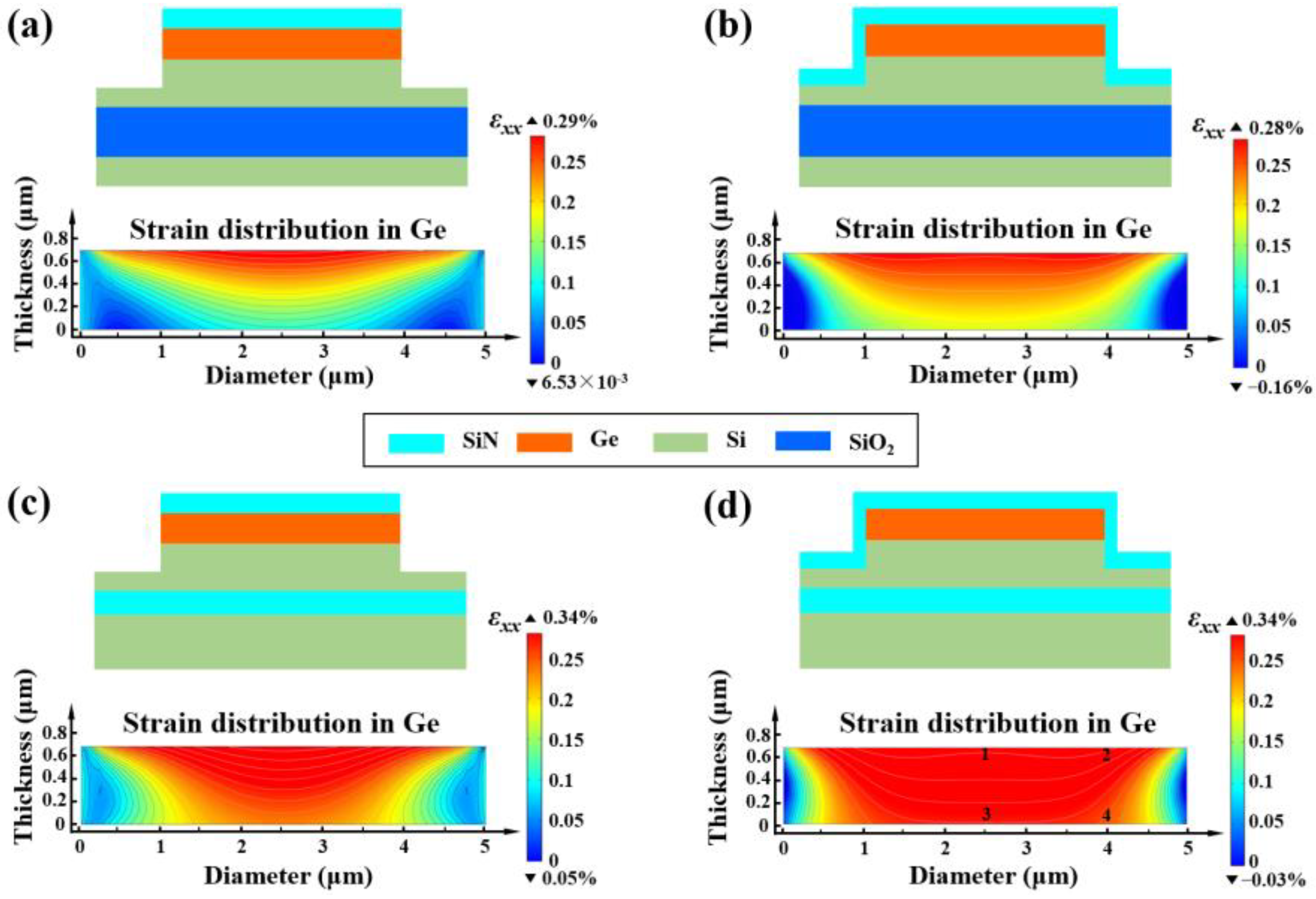
Figure 2.
The introduced strain εxx values in regions 1–4 for different thickness of (a) upper SiN stressor layer and (b) lower SiN stressor layer.
Figure 2.
The introduced strain εxx values in regions 1–4 for different thickness of (a) upper SiN stressor layer and (b) lower SiN stressor layer.

Figure 3.
The strain profiles in Ge with (a) 10 µm mesa diameter and (b) 20 µm mesa diameters and (c) 30 µm mesa diameter. (d) The value of introduced strain in region 1–2 with various mesa diameters.
Figure 3.
The strain profiles in Ge with (a) 10 µm mesa diameter and (b) 20 µm mesa diameters and (c) 30 µm mesa diameter. (d) The value of introduced strain in region 1–2 with various mesa diameters.
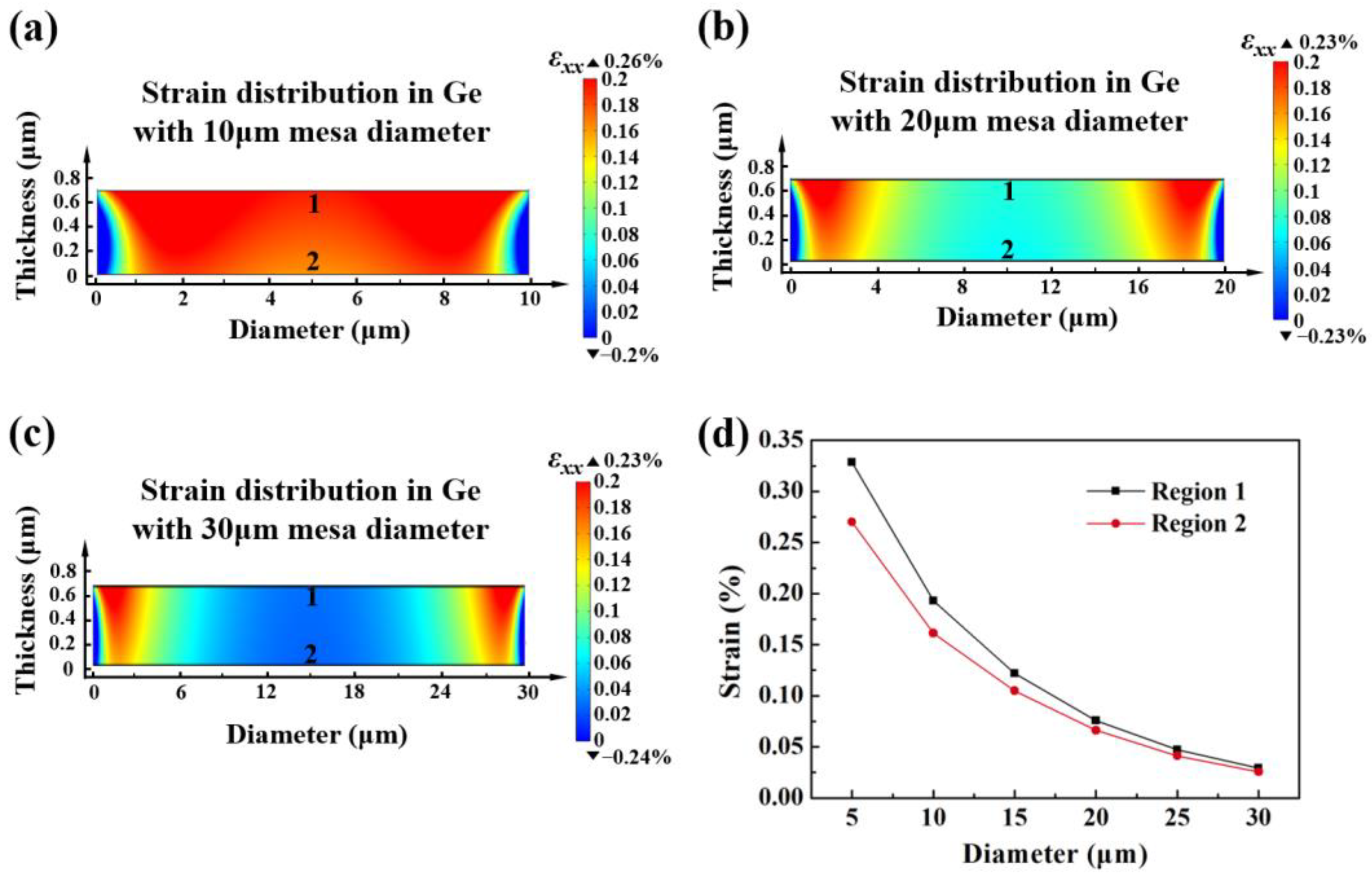
Figure 4.
3D schematic of the surface-illuminated SACM Ge/Si APD.

Figure 5.
(a) Photocurrent density of four types of devices vs. applied reverse bias voltage. (b) Dark current density and capacitance vs. applied reverse bias voltage.
Figure 5.
(a) Photocurrent density of four types of devices vs. applied reverse bias voltage. (b) Dark current density and capacitance vs. applied reverse bias voltage.
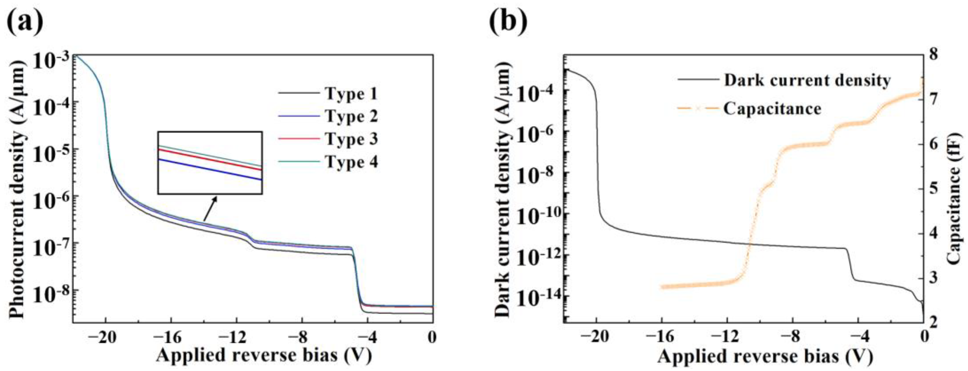
Figure 6.
The primary responsivity of (a) four device types at various wavelengths and (b) type 3 and type 4 with different thicknesses of ARC layer at 1.55 and 1.625 μm wavelength. (c) DC photoresponsivity and gain vs. applied reverse bias voltage characteristics of type 4 at 1.55 and 1.625 μm wavelength.
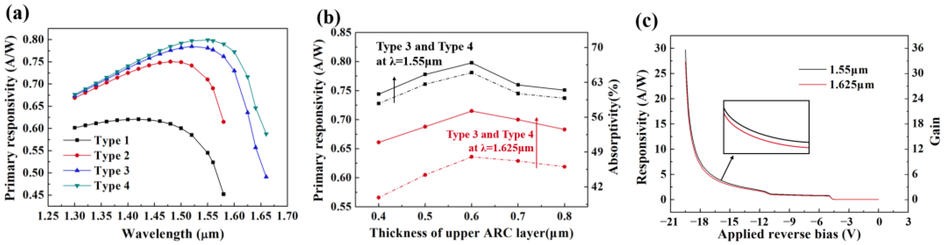
Figure 7.
(a) The primary responsivity and (b) 3-dB bandwidth of APDs based on type 3 and type 4 with different Ge absorption layer thicknesses (0.6, 0.7 μm, 0.8 μm).
Figure 7.
(a) The primary responsivity and (b) 3-dB bandwidth of APDs based on type 3 and type 4 with different Ge absorption layer thicknesses (0.6, 0.7 μm, 0.8 μm).

Table 1.
Four types of Ge/Si APDs with various structures.
| Type | Device Structure | RCE | SiN Stressor |
|---|---|---|---|
| 1 | Structure 2 | × | × |
| 2 | Structure 2 | √ | × |
| 3 | Structure 2 | √ | √ |
| 4 | Structure 4 | √ | √ |
Table 2.
Performance comparison of reported Ge/Si APDs.
| Ref. | λ (μm) | Device Type | Device Structure | Vbr (V) | Id (μA) | Rp (A/W) | Gain | f3-dB (GHz) | GBP (GHz) |
|---|---|---|---|---|---|---|---|---|---|
| [31] | 1.55 | Waveguide-integrated | Vertical SACM | −10 | 1 | 0.75 | 12 | 25 | 276 |
| [33] | 1.55 | Waveguide-integrated | Lateral SACM | −12 | 100 | 0.78 | 36 | 27 | 300 |
| [34] | 1.55 | Waveguide-integrated | Lateral PIN | −11 | 100 | 0.49 | 13 | 16 | 210 |
| [35] | 1.55 | Waveguide-integrated | Three-Terminal | −6 | 1000 | 0.48 | 15 | 18.9 | / |
| [7] | 1.55 | Surface-illuminated | Vertical SACM | −29.0 | 5 | 0.3 | 39 | 13 * | 310 |
| [28] | 1.55 | Surface-illuminated | Vertical SACM | −28.5 | 3 | 0.9 | 12 | 7 (M = 12) | 84 * |
| [36] | 1.55 | Surface-illuminated | Vertical SACM | −27 | 100 | 0.26 | 34.5 | / | / |
| This work | 1.55 | Surface-illuminated | Vertical SACM | −20.2 | 7.85 | 0.80 | 18 | 17.5 | 162 |
| 1.625 | 0.72 |
* These values were not clearly reported but were inferred from the reports.
Disclaimer/Publisher’s Note: The statements, opinions and data contained in all publications are solely those of the individual author(s) and contributor(s) and not of MDPI and/or the editor(s). MDPI and/or the editor(s) disclaim responsibility for any injury to people or property resulting from any ideas, methods, instructions or products referred to in the content. |
© 2022 by the authors. Licensee MDPI, Basel, Switzerland. This article is an open access article distributed under the terms and conditions of the Creative Commons Attribution (CC BY) license (https://creativecommons.org/licenses/by/4.0/).
Share and Cite
MDPI and ACS Style
Li, C.; Li, X.; Cai, Y.; Wang, W.; Yu, M. Design and Optimization of High-Responsivity High-Speed Ge/Si Avalanche Photodiode in the C+L Band. Micromachines 2023, 14, 108. https://doi.org/10.3390/mi14010108
AMA Style
Li C, Li X, Cai Y, Wang W, Yu M. Design and Optimization of High-Responsivity High-Speed Ge/Si Avalanche Photodiode in the C+L Band. Micromachines. 2023; 14(1):108. https://doi.org/10.3390/mi14010108
Chicago/Turabian StyleLi, Chuan, Xinyu Li, Yan Cai, Wei Wang, and Mingbin Yu. 2023. "Design and Optimization of High-Responsivity High-Speed Ge/Si Avalanche Photodiode in the C+L Band" Micromachines 14, no. 1: 108. https://doi.org/10.3390/mi14010108
Note that from the first issue of 2016, this journal uses article numbers instead of page numbers. See further details here.