Article

Impact of Nitridation on Bias Temperature Instability and Hard Breakdown Characteristics of SiON MOSFETs

IMEC, Kapeldreef 75, 3001 Leuven, Belgium
*
Author to whom correspondence should be addressed.
Micromachines 2023, 14(8), 1514; https://doi.org/10.3390/mi14081514
Submission received: 30 June 2023 / Revised: 24 July 2023 / Accepted: 26 July 2023 / Published: 28 July 2023
(This article belongs to the Special Issue Reliability Issues in Advanced Transistor Nodes)

Abstract

:
We study how nitridation, applied to SiON gate layers, impacts the reliability of planar metal-oxide-semiconductor field effect transistors (MOSFETs) subjected to negative and positive bias temperature instability (N/PBTI) as well as hard breakdown (HBD) characteristics of these devices. Experimental data demonstrate that p-channel transistors with SiON layers characterized by a higher nitrogen concentration have poorer NBTI reliability compared to their counterparts with a lower nitrogen content, while PBTI in n-channel devices is negligibly weak in all samples independently of the nitrogen concentration. The Weibull distribution of HBD fields extracted from experimental data in devices with a higher N density are shifted towards lower values with respect to that measured in MOSFETs, and SiON films have a lower nitrogen concentration. Based on these findings, we conclude that a higher nitrogen concentration results in the aggravation of BTI robustness and HBD characteristics.

1. Introduction

The breath-taking development of micro- and nanoelectronics relies on the rapid scaling of the metal–oxide–semiconductor field effect transistor (MOSFET) based on silicon. To meet requirements dictated by mobile/portable electronic products and applications for long battery lifetimes and hence reduced OFF-currents and optimized ON/OFF-current ratio, novel transistor architectures—starting from planar devices and going to 3D geometries such as finFETs [1,2] and continuing to nanosheet [3,4], forksheet [5,6,7], and complementary FETs [8,9]—have been introduced. However, before the launching of any new transistor node, its reliability characteristics should be carefully assessed together with the performance, power consumption, etc. Among reliability issues featured by modern MOSFETs, the most detrimental ones are bias temperature instability (BTI) [10,11], time-dependent dielectric breakdown/hard breakdown (TDDB/HBD) [12,13], and hot-carrier degradation (HCD) [14,15,16]. Although HCD has been repeatedly flagged as a very severe degradation concern in confined 3D transistor architectures [17,18], it lies outside the scope of this paper. The reason for that is that BTI and HBD are intimately linked with the gate stack quality, while HCD is rather related to carrier acceleration by the electric field, which is determined by the voltage partition in the transport (i.e., source-drain) direction [19,20,21,22,23,24]. Therefore, rather than focusing on the device architecture optimization aiming to mitigate HCD, the focus of this work is put on optimization of SiON layers to suppress such reliability issues as BTI and HBD.
Among various techniques aimed at alleviating BTI and improving breakdown characteristics of the gate stack, nitridation of the gate dielectric layers has been the subject of extensive studies performed by several groups. Regarding the impact of nitridation on TDDB/HBD, to the best of our knowledge, there are a very limited number of publications addressing this subject. Among them, are the papers by Joo et al. [25] and Mazumder et al. [26], which analyzed how nitridation in NO 2 ambient impacts TDDB and concluded that low-pressure nitridation results in the improvement of TDDB robustness, while nitridation at an increased pressure leads to poorer TDDB characteristics. A TDDB lifetime improvement due to annealing in the NO ambience was reported by Chen et al. [27], while Lee et al. [28] demonstrated that ex situ N annealing has a very weak impact on TDDB. Therefore, one can summarize these studies, and depending on nitridation conditions, this fabrication step can either improve TDDB/HBD robustness or aggravate it.
Very similar to the case of TDDB/HBD, a consensus regarding the impact of nitridation on BTI reliability has not been reached so far. On the one hand, several groups suggest that the incorporation of N into a gate stack suppresses BTI. Thus, O’Sullivan et al. demonstrated that N (or F) diffusion into the gate dielectric layer can shift the band of donor-like traps, thereby impeding negative BTI (NBTI) [29]. In [30], O’Connor et al. reported that N passivates traps in HfSiO layers but this behavior can be reversed during stress, thereby giving rise to NBTI and a stress-induced leakage current (which accompanies TDDB). Further, Maheta et al. [31] speculated that the impact of N on NBTI is very intricate and is comprised of changing properties of interface traps and oxide states, thereby resulting in different characteristic energies for trap activation and NBTI time exponents. Joshi et al. [32] published a reduction of BTI due to N incorporation. On the other hand, Garros et al. claimed that in their MOSFETs with high-k/metal gate stacks N results in severe aggravation of BTI reliability [33,34]. Their results are consistent with data published by Reisinger et al., which demonstrate stronger NBTI in nitrided oxides compared to non-nitrided ones [35]. Finally, Takasaki et al. [36] used the charge-pumping technique to resolve the interface trap density in devices with different parameters of the nitridation process subjected to BTI stress. Their results suggest that BTI aggravates transistors with a higher N content.
Renewed interest in BTI and HBD reliability of MOSFETs with nitrided gate oxides is related to the introduction of the forksheet transistor architecture, where n- and pFET sheets are separated by an Si 3 N 4 (or SiON) wall. Recent experimental studies of reliability issues in forksheet FETs did not show extra charge trapping in the Si 3 N 4 (or SiON) wall [37]. From the simulation perspective, this behavior was explained to be exclusively due to electrostatic reasons, i.e., the corresponding voltage partition in the forksheet wall [38]. However, for further boosting device reliability, it is important to understand whether N incorporation into SiO 2 and SiON films improves or aggravates transistor robustness. Moreover, the knowledge on the reliability of SiON gate stacks acquired in this work should also be of relevance for novel FET architectures employing SiON related materials outside their gate stack, e.g., in the forksheet FET wall, transistor spacers, etc.
Therefore, the scope of this paper is an experimental investigation on the impact of nitridation of gate SiON layers on BTI and HBD characteristics. We also aim at contributing towards reconciling controversies regarding the impact of nitridation on gate oxide reliability.

2. Devices

We employed planar n- and p-channel MOSFETs fabricated in a 300 mm line using a standard gate first flow. These transistors have a gate stack made of an SiON layer and a 100 nm polySi layer deposited in situ. To fabricate the SiON layer, first an SiO 2 film was grown by steam generation in a rapid thermal processing system and then this film was subjected to nitridation in the N 2 ambient, followed by a post-nitridation anneal. We used two types of nitridation processes:
  • The process of reference (POR), which includes plasma nitridation at a higher value of the radio frequency (RF) power of 1000 W under a pressure of 20 Torr for 12 s.
  • The alternative process with softer nitridation (SN) conducted at a lower RF power of 900 W under a pressure of 20 Torr for 12 s.
Let us emphasize that these two transistor splits are close to each other, but we have a narrow device target window specified by the targeted equivalent oxide thickness (EOT), the gate leakage current density, etc. Therefore, in order to ensure that these splits fit into the specified window, we were limited in variations of the fabrication process parameters.
Devices with a targeted physical thickness of the SiON layer of 1.9 nm were fabricated using both the POR (this sample is labeled as “S #1”) and the process including the SN step (this sample is labeled as “S #2”), see Table 1. In addition to this, MOSFETs with a 2 Å thicker SiON layer (targeted physical thickness is 2.1 nm) were fabricated by the POR, (S #3, Table 1). Finally, with the SN-based process, transistors with a 2 Å thinner SiON film (targeted thickness is 1.7 nm, S #4 and 5) were also grown. The EOT values for all samples, obtained using capacitance-voltage measurements combined with the CVC model for EOT extraction [39], are summarized in Table 1. Within the EOT extraction procedure, the potential partition in the depleted poly-Si layer and correction due to quantum confinement at the Si/SiON interface were taken into account.
Threshold voltage values were extracted from transfer characteristics ( I d V g , where I d is the drain current and V g is the gate voltage) using the maximum transconductance method; see Table 1. From Table 1, it can be observed that although samples S #4 and S #5 have the same targeted thickness, which is 2 Å less than that of the POR device (sample S #1), in practice, their EOT is comparable to the EOT of the reference sample (sample S #1). In addition, their V t values substantially deviate from those of other samples. As a consequence, one can expect that S #4 and S #5 have an inferior reliability among the entire set of devices.
The extracted threshold voltage values are consistent with the parameters of the nitridation step. Indeed, N incorporated in the gate dielectric is known to result in positive charges distributed throughout the layer, which, in turn, induce a threshold voltage shift towards lower values. Samples #1 and 2 have the same targeted physical thickness, but, in the latter case, nitridation was carried out with lower power; therefore, S #2 has a lower N content compared to S #1. The corresponding V t voltages are consistent with this trend, i.e., V t values of S #2 are higher for both n- and pMOSFETs as compared to those of S #1. The wafers S #4 and 5 were fabricated by the same process as S #2, but the physical thickness of their SiON layers is the lowest among all devices used in this study; therefore, they have the highest concentration of nitrogen and hence the lowest values of V t . Finally, for S #1 and 3, the same nitridation process was employed; however, the wafer S #3 has a 2 Å thicker SiON layer and therefore a lower N content and higher threshold voltages. A summary of N content can be found in the last column of Table 1, where a higher rank corresponds to a higher concentration, i.e., ‘1’ corresponds to the lowest N content and ‘4’ to the highest N concentration.
We would like to note that although a comparison of BTI and HBD characteristics of MOSFETs with SiON films against those acquired in devices with pure SiO 2 as a gate dielectric would be informative, such a comparison was not performed in this study. The reason for that is that the reliability measurements were carried out to qualify the gate oxide integrity for the 65 nm technology node with polySi/SiON gate stack. Therefore, in this EOT range (see Table 1), it is required to employ SiON as high-k dielectric to ensure lower gate leakage and better electrostatic control of the channel. Consequently, we do not have SiO 2 -based MOSFETs at our disposal.

3. Experiment and Data Processing

In ultra-scaled FETs, characteristics of pristine devices can vary from sample-to-sample. This is called “time-zero variability” [40], which originates from several sources such as random dopant fluctuations, metal gate granularity, line edge roughness, fluctuations in material properties, oxide thickness variations, etc. [41,42,43,44,45,46]. Degradation of device characteristics is due to generation/activation of defects. Ultra-scaled FETs contain just a handful of defects (and their precursors), which are randomly distributed throughout a transistor; therefore, contributions of individual defects to degradation can be discernible. Thus, BTI and HCD types of stress leads to time-dependent variability in small-area MOSFETs [47,48,49]. In contrast, in large-area devices, BTI/HCD is due to a collective response of a very large number of defects, and a sample-to-sample scattering of degradation characteristics is not prominent. Hence, in order to avoid BTI-induced variability, we intentionally chose large-area devices. Regarding TDDB/HBD, this type of degradation is driven by defect build-up across the dielectric film resulting in the formation of a percolation path. Hence, for the processing/interpretation of experimental HBD data, stochastic approaches are typically employed for both large- and small-area devices [12,50]. To summarize, for BTI and HBD measurements, we chose MOSFETs with a gate length ( L g ) and a width (W) of 1 μm.
The studied samples were subjected to ramped voltage stress (RVS) in BTI and HBD regimes at room temperature. For both degradation modes, we used the RVS technique developed by Kerber et al. [51,52]. Note that for BTI, the extended measure–stress–measure procedure (eMSM) [53] is commonly employed, while for HBD studies, the standard routine is constant voltage stress (CVS) [54,55,56]. Despite the fact that the eMSM and CVS techniques provide a more comprehensive insight into BTI and HBD, respectively, the RVS scheme was proven to have same accuracy for both BTI [51,52] and TDDB/HBD [57] degradation modes. On the other hand, the RVS technique allows us to dramatically reduce the experimental time, thereby making itself the routine of choice for conducted BTI and HBD investigations.
In these experiments, n-channel transistors were stressed under positive gate bias V g (in both BTI and HBD regimes), while their p-channel counterparts were subjected to RVS stress at negative V g .

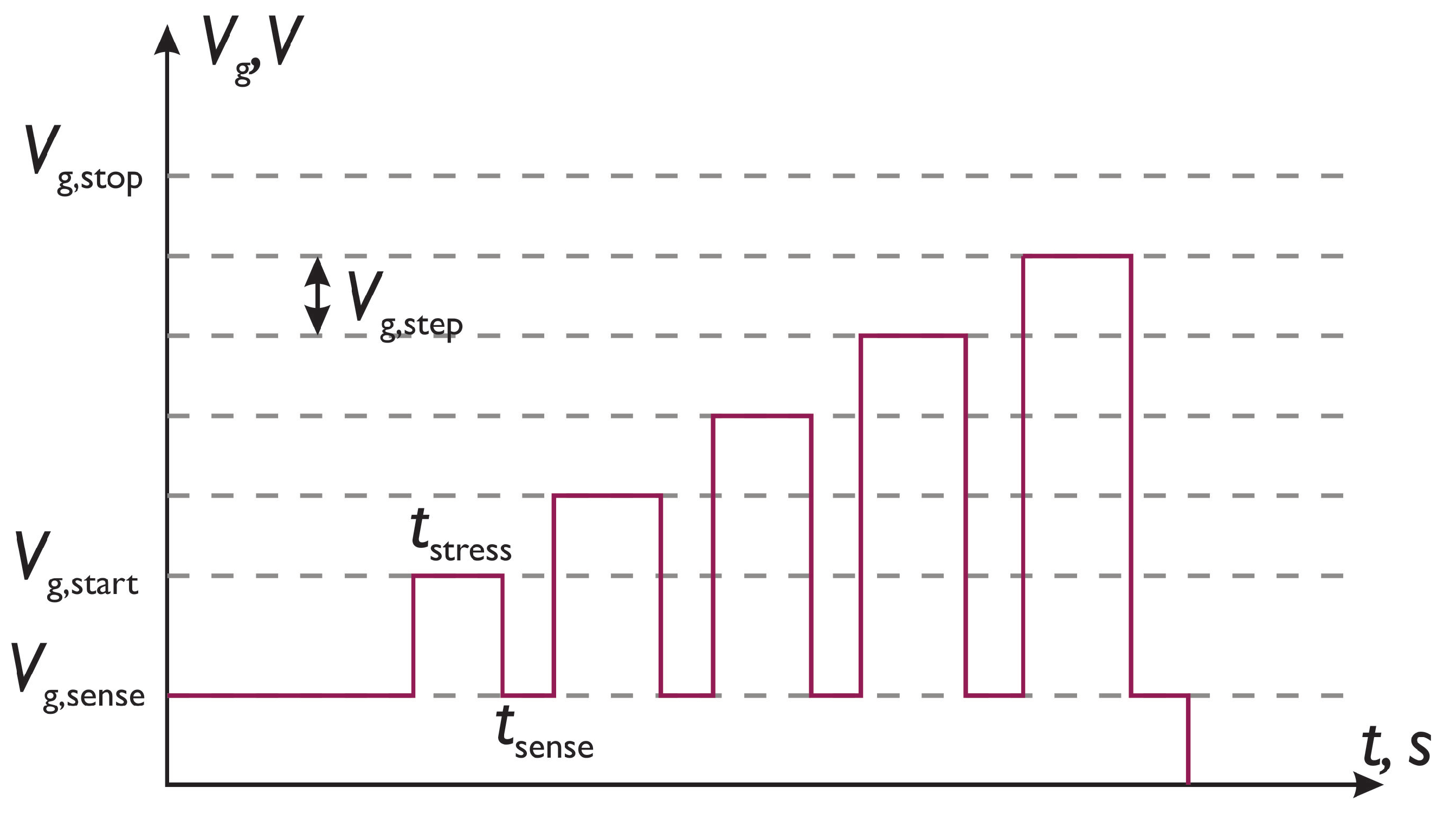
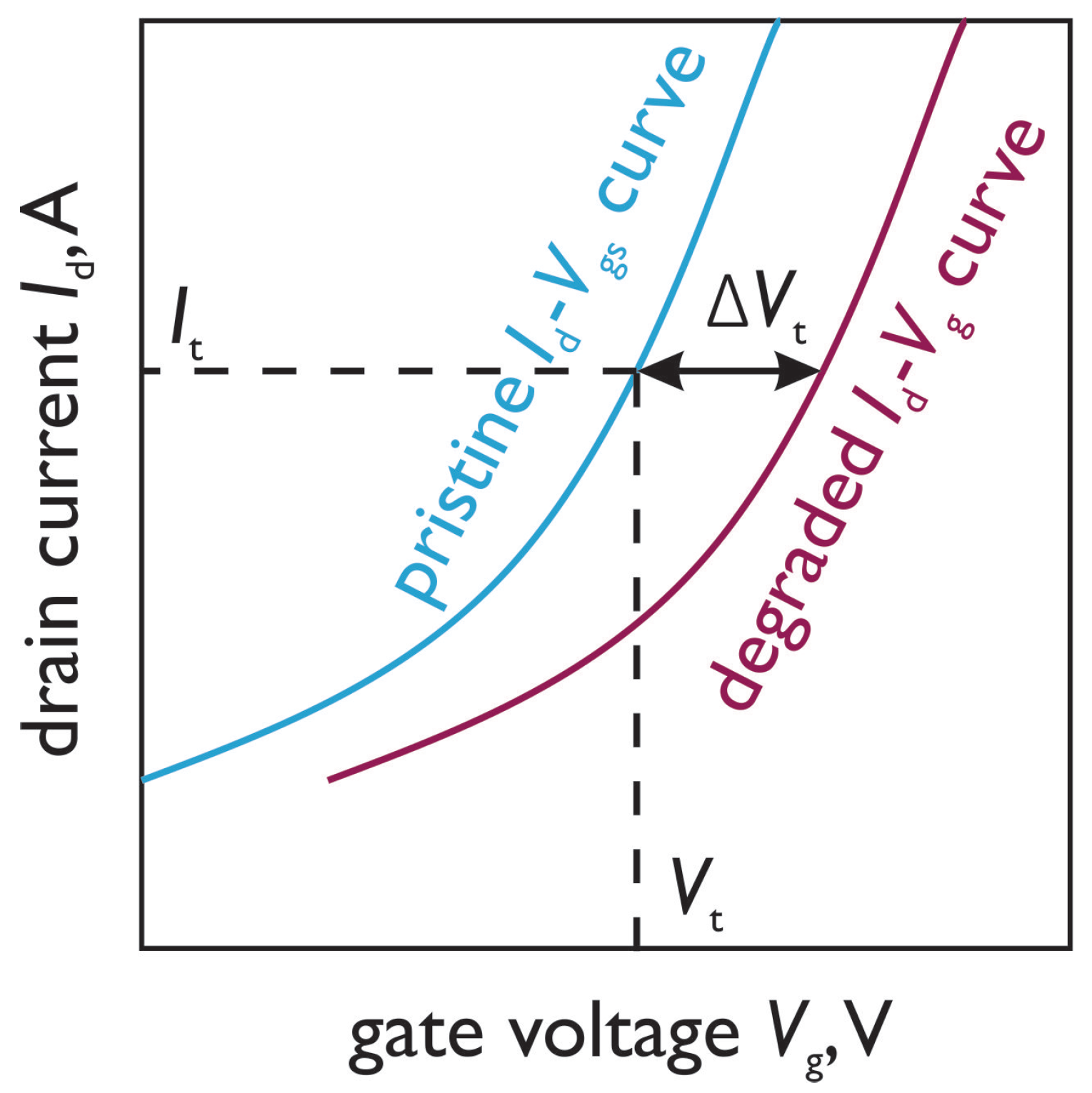
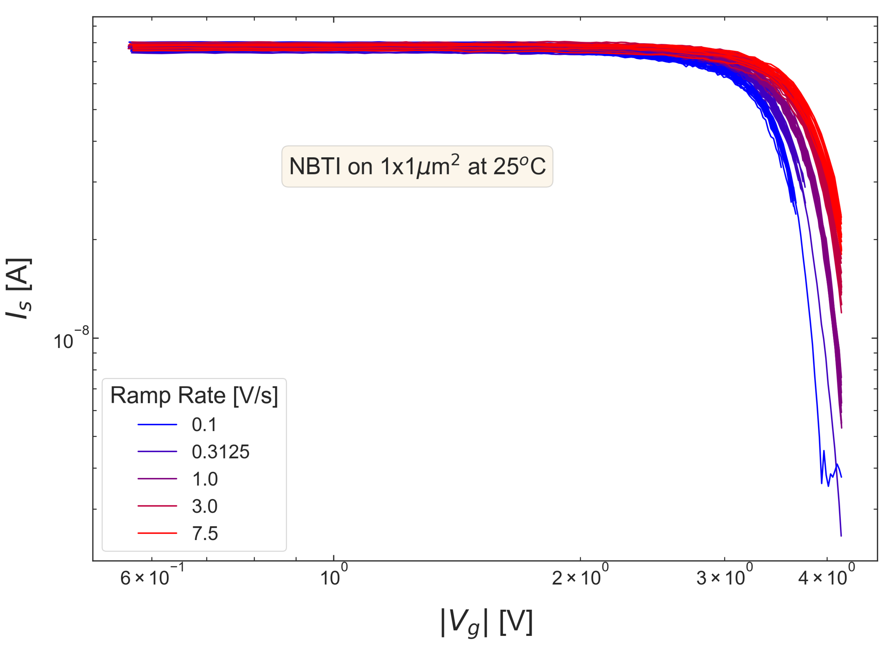
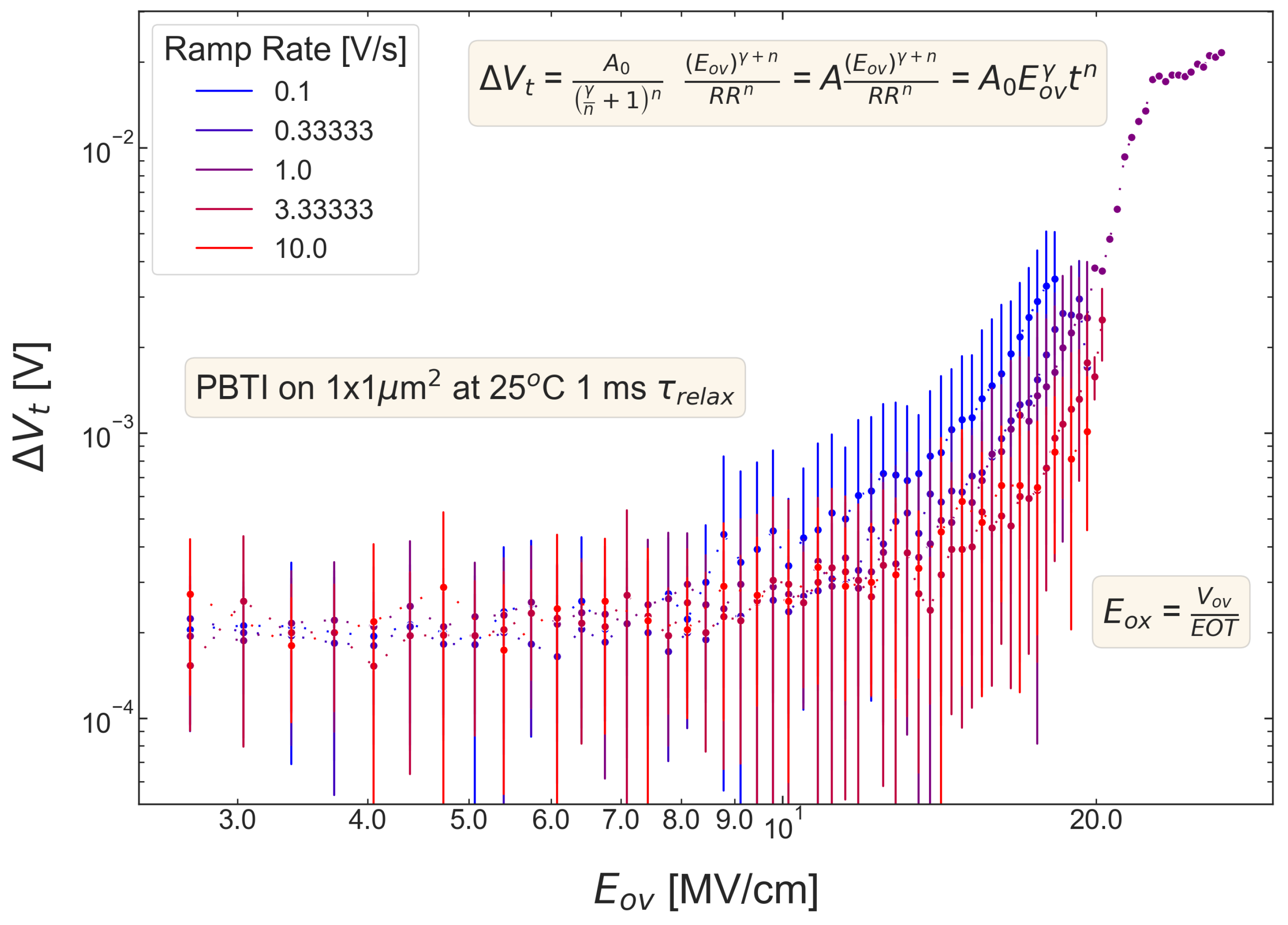
3.1. Bias Temperature Instability
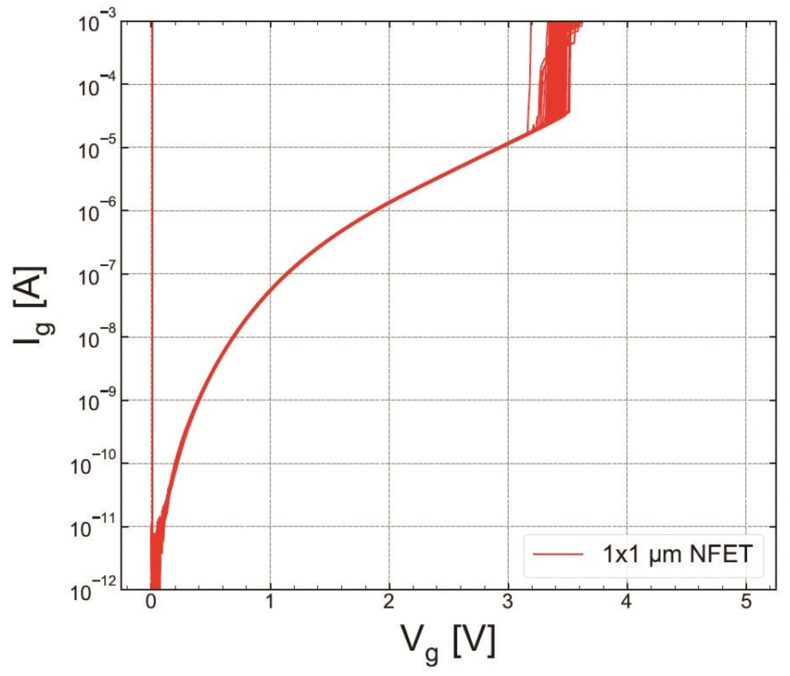
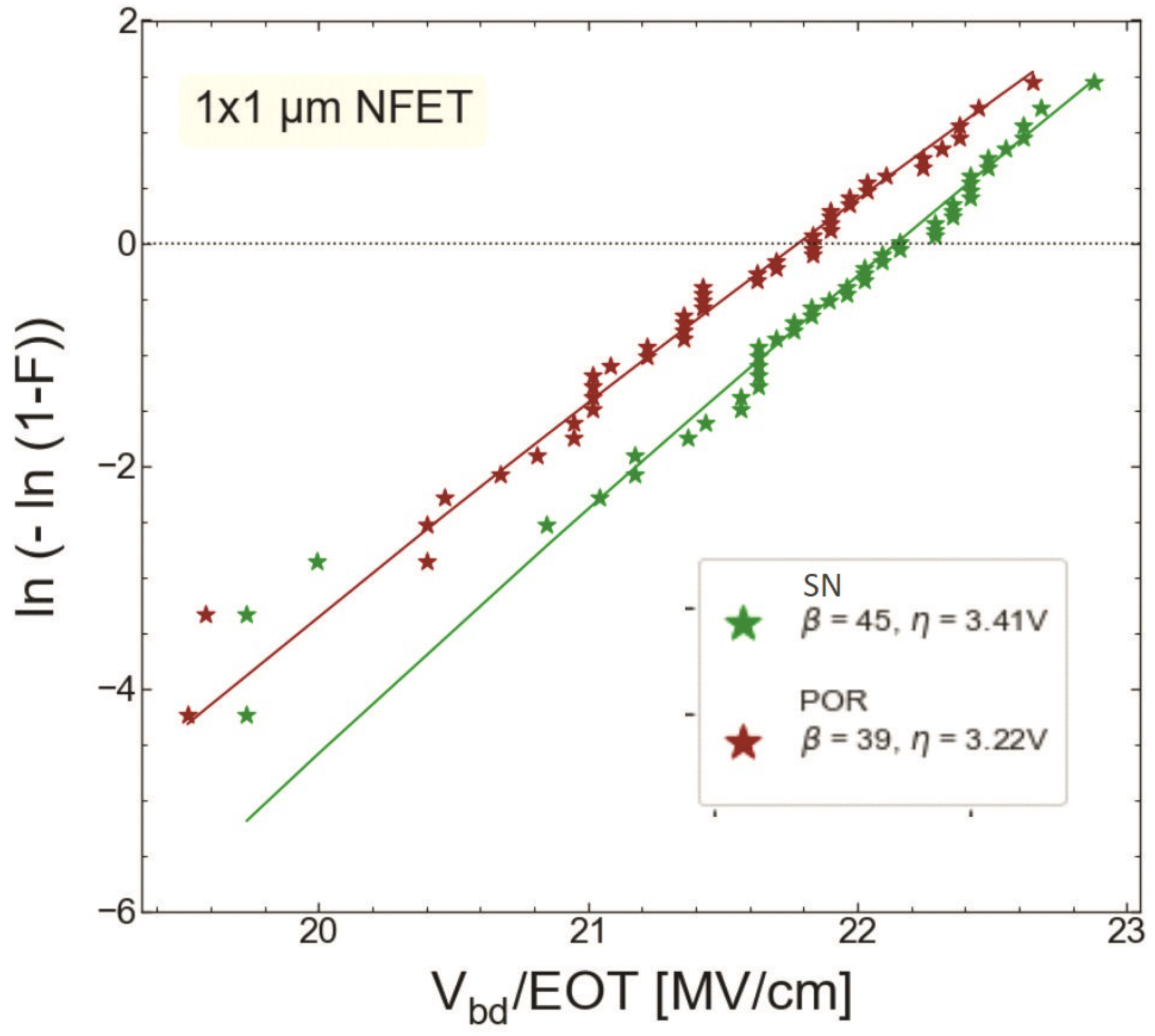
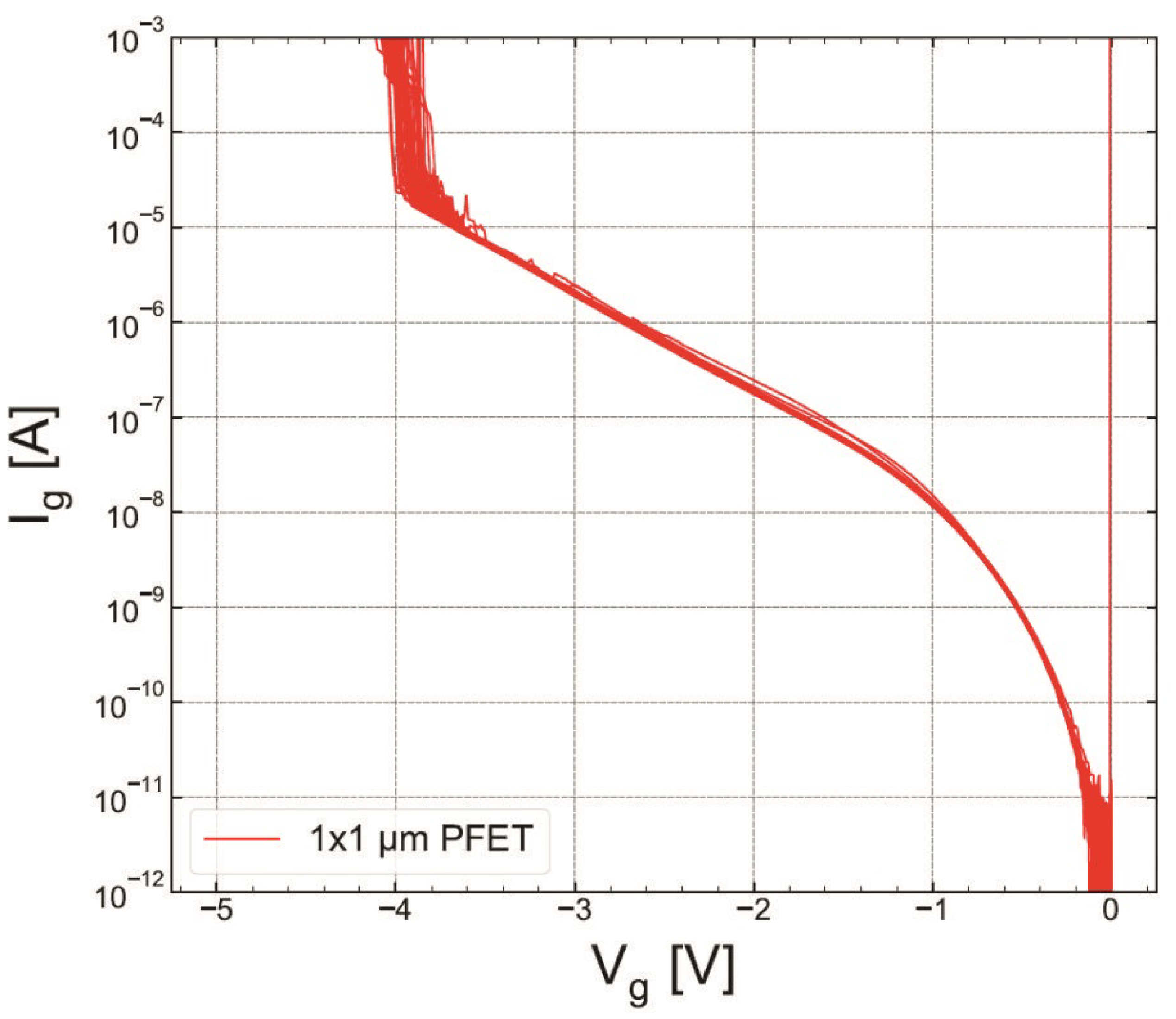
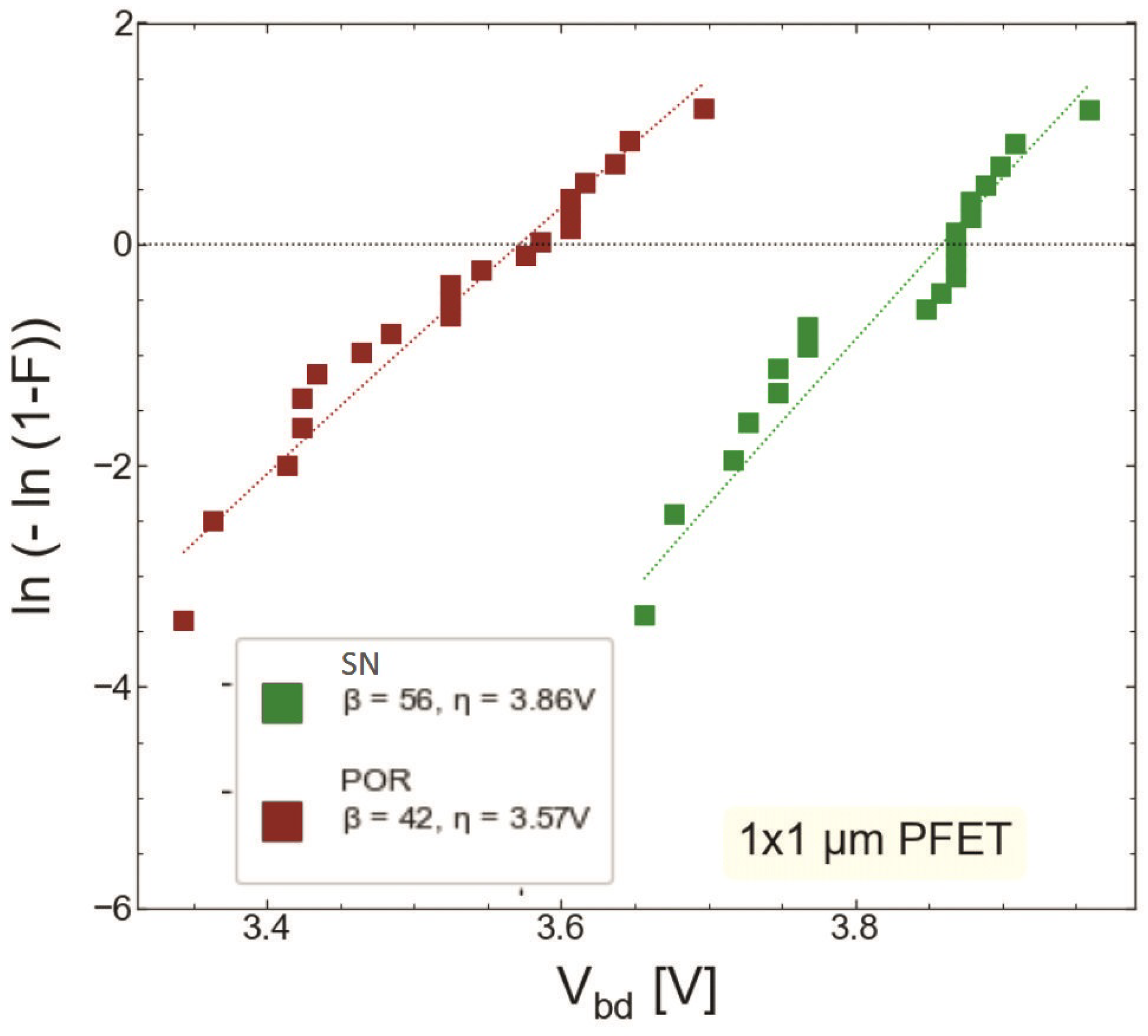
The RVS measurement procedure for BTI, which is comprised of sense and stress phases, is schematically depicted in Figure 1. Prior to BTI stress, I d V g curves in a limited V g range (we used | V g | sweeping the range of [0; 1.0] V) of pristine transistors were measured. I d V g characteristics were then employed to extract the V t value and the corresponding drain current I t = I d ( V g = V t ) . Next, we applied a stress pulse of a duration of t stress with an increasing amplitude: for the stress phase i, the signal amplitude is V g,start + i × V g,step . These ramps sweep the voltage range of [ V g,start ; V g,stop ], increasing the amplitude each time by V g,step , see Figure 1. Each stress phase labeled with i is followed by a phase (with the same index i) when we interrupt the stress and extract V t .
V t is determined as the gate voltage which satisfies the criterion: I t = I d ( V g ) ; see Figure 2. The obtained value is V t ( t ) , with t being the cumulative stress time: t i × t stress . Therefore, the stress-induced shift in the threshold voltage is determined as Δ V t = | V t ( t ) V t ( 0 ) |. Another important parameter of the RVS routine is the ramp rate R R = V g,step / t stress . It is noteworthy that a lower R R , ceteris paribus, results in a larger Δ V t . This is because the stress time at each voltage step is longer for the slower ramp rate (i.e., if the V g,step value is constant and t stress is longer, then their ratio V g,step / t tstress , defined as R R , is lower). For each R R value and type of MOSFETs (i.e., n- and p-channels and the fabrication process flow) we used eight samples.
For NBTI measurements, we used the following parameters: V g,start = V t 0.4 V, V g,stop = V t 4.0 V; the voltage step V g,step and the pulse duration t stress were chosen to ensure five different ramp rates of 0.1, 0.3, 1.0, 3.0, and 7.5 V/s. The drain voltage V d was set to −0.05 V. PBTI measurements were conducted in a similar fashion with V g,start = V t + 0.4 V, V g,stop = V t + 4.0 V, and R R = 0.1, 0.3, 1.0, 10.0, and 3.3 V/s; V d = 0.05 V.
To process BTI data acquired using the RVS routine, we assume the following Δ V t dependency on the stress time and gate bias:
Δ V t A 0 | V g V t ( 0 ) | t ox γ t n = A 0 | V ov | t ox γ t n = A 0 E ov γ t n ,
where A 0 is a prefactor (accounting for the thermal activation of the BTI process), t ox is the EOT of the gate dielectric layer, V ov = V g V t is the overdrive voltage, E ov = V ov / t ox , while n and γ are exponents determining time dependency and field acceleration of BTI, respectively. According to Kerber et al. [51,52], this formula can be rewritten in a manner to link Δ V t to the ramp rate R R :
Δ V t = A 0 γ n + 1 n E ov R R n .
Therefore, if the threshold voltage shift was measured as a function of V ov / E ov and the R R , its time dependency can be extracted.

3.2. Hard Breakdown

In case of HBD, we used the scheme very similar to the RVS BTI measurement routine. However, instead of the sense phase, we monitored the gate leakage current I g . In order to detect an HBD event, which manifests itself by an abrupt increase in the gate current observed at a stress voltage V BD , we aimed at sweeping the [ V g,start ; V g,stop ] range with the minimum V g,step available at our measurement setup. Therefore, for HBD in nMOSFETs, we employed V g,start = 0.0 V, V g,stop = 5.0 V, and V g,step = 0.01 V; for the ramp rate, we used a single value of R R = 0.09 V/s. pMOSFETs were stressed at V g,start = 0.0 V, V g,stop = 5.0 V. In all cases V d = 0 V. For acquiring a comprehensive statistical set required for the extraction of the breakdown voltage distribution, we used 48 samples for each channel polarity and type of transistors (summarized in Table 1).
Extracted V BD values are then binned into a Weibull distribution. First, using the Bénard approximation [58], we calculate probabilities F i = F i ( V BD , i ) and then convert them to weibits W i . Next, we fit the W ( V BD ) dependency with a Weibull distribution and extract its parameters β (the shape factor) and η (the scale factor). To achieve this goal, we use the maximum likelihood estimation method.

4. Results and Discussion

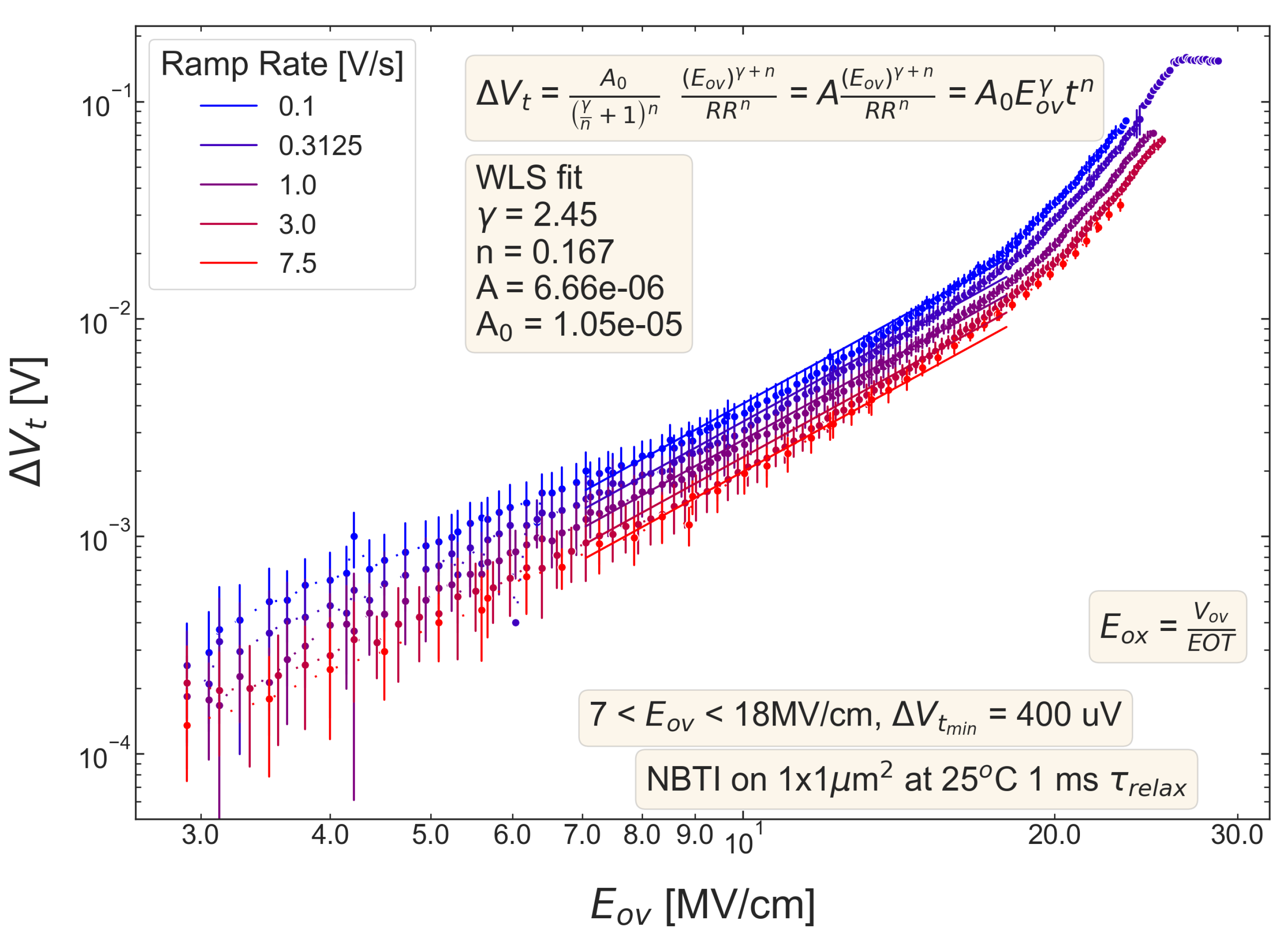
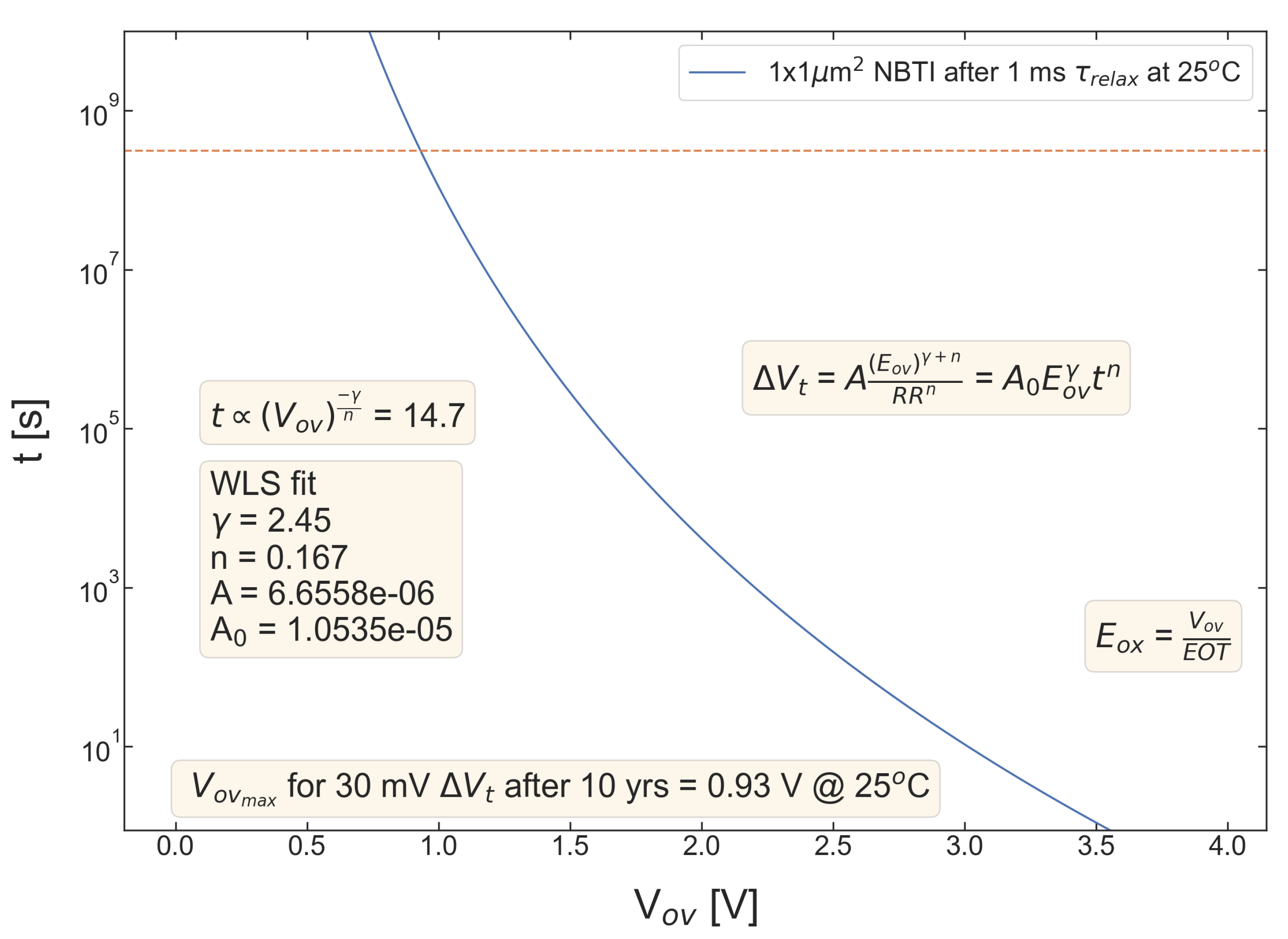
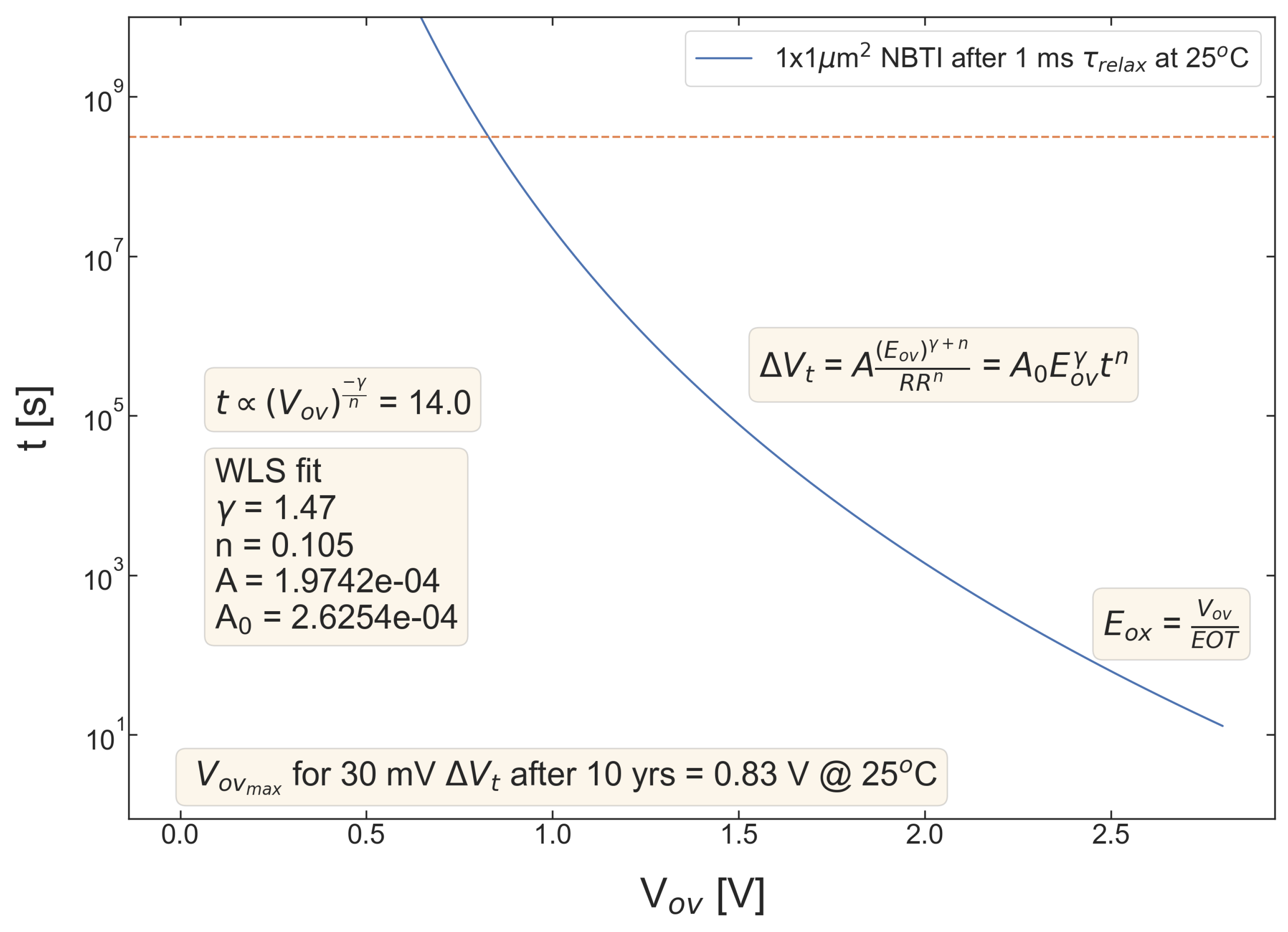
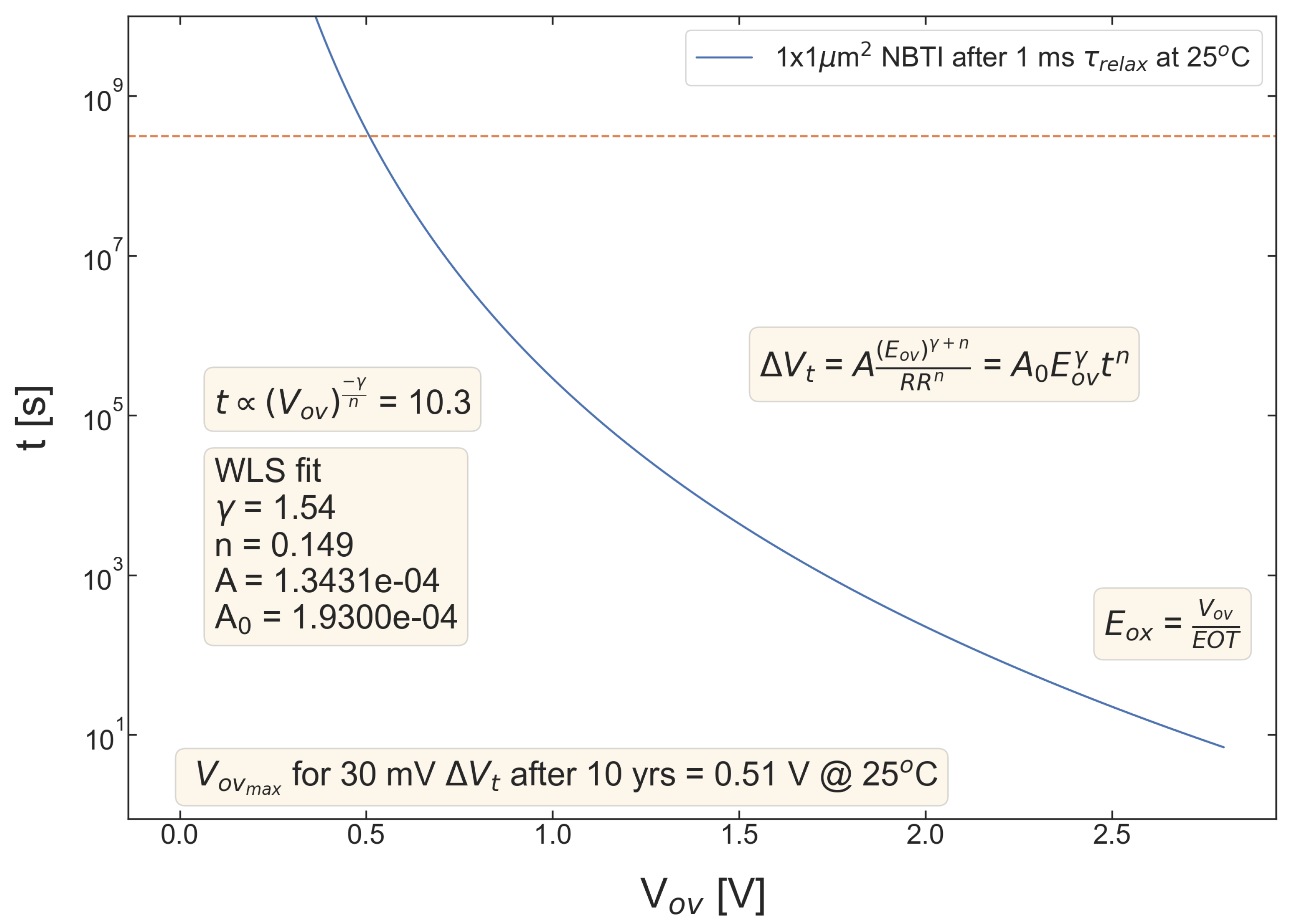
4.1. Bias Temperature Instability
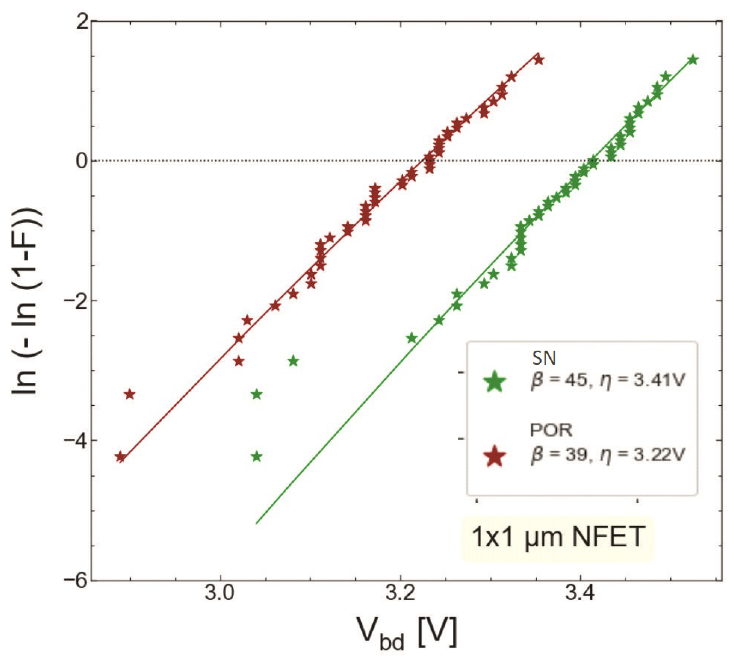
In RVS BTI measurements, at each sense phase, we recorded the drain current I d and plotted I d values as a function of stress voltage V g . An example of these I d traces obtained during NBTI stress for the pMOSFET fabricated using soft nitridation and with the targeted SiON thickness of 1.9 nm (wafer S #2) is given in Figure 3. The degradation of the device performance manifests itself by I d reduction, and, this reduction, as discussed before, becomes more pronounced at lower ramp rates. The recorded I d dependencies allowed us to extract threshold voltage shifts Δ V t for each sense phase.
For all five pMOSFETs subjected to NBTI, dependencies of the threshold voltage Δ V t shift on E ov = V ov / t ox are shown in Figure 4, Figure 5, Figure 6, Figure 7 and Figure 8. Δ V t changes are mean values obtained by averaging over the entire ensemble of eight Δ V t ( E ov ) curves measured at a given R R rate. In Figure 4, Figure 5, Figure 6, Figure 7 and Figure 8, the error bars for threshold voltage changes are also shown; we conclude that although standard deviations of Δ V t ( E ov ) values are discernible, they are small. One can observe that Δ V t values become larger at lower ramp rates and this trend agrees with Equation (2). Another pronounced peculiarity is that at high electric fields of E ov 20 MV/cm, the slope of Δ V t ( E ov ) dependencies increases; this behavior is typical for all considered samples. Such a peculiarity is most probably related to non-equilibrium BTI driven by electrons traveling in the SiON conduction band, which can gain substantially high energies due to acceleration by the electric field and induce hydrogen release at the SiON/Si interface. Generation of interface traps according to this scenario was reported by the group from IBM [59,60] and recently by Bastos et al. [61]. However, this process occurs at very high electric fields and is related to another physical mechanism than that responsible for “conventional” BTI. Hence, we do not consider this degradation scenario while extracting device time-to-failure (TTF). It is worth mentioning that BTI measurements continued up to high V g values, and before reaching these voltages most of the devices broke down. During the processing of BTI data, we applied a filtering of HBD-induced current jumps; therefore, HBD events are not pronounced in Figure 4, Figure 5, Figure 6, Figure 7 and Figure 8.
Experimental Δ V t ( E ov ) curves were captured by Formula (2) and the exponents γ and n were extracted; from Figure 4, Figure 5, Figure 6, Figure 7 and Figure 8, it can be observed that the agreement is good. For the fitting procedure, we employed the weighted linear regression method. Note that under a considerable threshold voltage shift, we assume Δ V t 1 mV; therefore, V t values below this level were down-weighted. This also resulted in a more narrow—compared to the range determined by the used V g,start and V g,stop values (Figure 1)– E ov range. For instance, one can observe that for S #2 (Figure 5) we carried out fitting for E ov 7 MV/cm because at lower fields the threshold voltage shift is below 1 mV, i.e., negligibly small. In contrast, NBTI demonstrated by samples S #4 and 5 is much more significant; therefore, we could fit experimental data without limiting the E ov range at the low value side. We also avoided the aforementioned E ov region with a higher slope of the Δ V t ( E ov ) curve (e.g., for S #1, this change is visible at E ov 17 MV/cm, see Figure 4). Considering this E ov range would result in an overestimated TTF value, which is determined as a stress time at which Δ V t reaches a margin of 30 mV. This is because we extract the device lifetime by extrapolating the dependency of Δ V t on V ov (or E ov ) from the experimentally available range to cover the operating voltage ( V dd ) value. However, a steeper Δ V t ( V ov ) curve would result in a smaller Δ V t ( V dd ) shift and hence larger TTF.
From Figure 4, Figure 5, Figure 6, Figure 7 and Figure 8, one can observe, that, as expected (see Section 2), devices S #4 and 5 have poor NBTI characteristics, i.e., relatively high Δ V t values already at a low E ov ; the most gradual slope of Δ V t ( E ov ) curves determined by the parameter γ . On the contrary, the MOSFET S #2, which received soft nitridation and has a larger physical thickness of SiON than S #4 and 5, features the best NBTI reliability throughout the entire sample selection: negligibly small Δ V t shift up to E ov 8 MV/cm and the largest value of the exponent γ . If we compare S #1 and S #3, which have the same process flow but differ in the targeted physical thickness, one can observe that the latter one (with a lower N content) has substantially better NBTI reliability. Based on data presented in Figure 4, Figure 5, Figure 6, Figure 7 and Figure 8, we conclude that MOSFETs with a lower N concentration (see Table 1) in their SiON layers demonstrate superior NBTI behavior.
Figure 9, Figure 10, Figure 11, Figure 12 and Figure 13 summarize stress time values t corresponding to Δ V th = 30 mV plotted as a function of V ov for all devices. These curves allow us to determine the upper limit of the safe operating area of these devices, as the V ov value of each device lifetime is equal to 10 years. As consistent with the data set from Figure 4, Figure 5, Figure 6, Figure 7 and Figure 8, S #4 and 5 have the lowest V ov ( t = 10 yrs ) voltages, while S #2 is again the winner. More general, MOSFETs with a lower nitrogen content have longer TTF values.
PBTI stress was applied to nMOSFETs. Figure 14 summarizes Δ V t ( E ov ) curves obtained using samples from the wafer with the SiON film, which was grown by the POR and has the targeted thickness of 1.9 nm (S #1). It is pronounced that at low electric fields, Δ V t values hardly overcome the noise level, and values measured at different ramp rates are not discernible. Even at such a high field as E ov = 20 MV/cm, the threshold voltage shift reaches a level of 4 mV, thereby suggesting that PBTI is very weak. Due to this reason, we perform neither a fitting of Δ V t ( E ov ) with Equation (2) nor an extraction of the V ov corresponding to TTF of 10 years at the margin of Δ V t = 30 mV. Let us emphasize that this behavior is typical for all samples examined in this work (data are not shown). Therefore, we can conclude that in all these nMOSFETs, the PBTI is negligibly weak; therefore, we cannot judge which samples demonstrate superior PBTI reliability.
Note that weak PBTI in nMOSFETs is very typical for transistors with silicon oxides/nitrides [10]. This can be explained assuming that the physical mechanism underlying BTI is the capture/emission of charge carriers by/from traps in the dielectric layer [11], and, in the case of PBTI in n-channel FETs with SiO 2 / SiON / SiN gate dielectric layers, the energetical position of the trap band is so that these traps are not accessible for the carriers (which are inversion electrons in the case of PBTI in nMOSFETs) [62].

4.2. Hard Breakdown

We compared HBD experimental data sets obtained only for MOSFETs with the targeted thickness of 1.9 nm fabricated by the POR (S #1) and with the SN step (S #2). Figure 15 and Figure 16 show the gate current I g as a function of stress gate voltage V g for n-channel transistors from wafers S #1 and S #2, respectively. Gate voltage values corresponding to HBD events ( V BD ) were extracted and binned into distributions, which are represented as Weibit plots in Figure 17. One can observe that the Weibull distribution of ( V BD ) extracted for the transistor fabricated by the SN process is shifted by 0.2 V towards higher voltages compared to that obtained for the POR MOSFET. However, these samples have slightly different EOT values; therefore, the Weibull distribution of the breakdown field E BD (the ratio between V BD and EOT) shown in (Figure 18) appears to be more informative. From Figure 18, we conclude that the POR nMOSFET has lower breakdown fields compared to their counterparts fabricated with the softer nitridation step.
As for RVS-HBD in pMOSFETs, I g ( V g ) dependencies for both POR and SN samples are shown in Figure 19 and Figure 20, respectively. The extracted V BD (Figure 21) and E BD (Figure 22) distributions confirm again that the SN sample has superior HBD robustness. However, the shift of the E BD distribution towards higher E BD values for the SN sample with respect to that extracted for the POR sample is not significant.

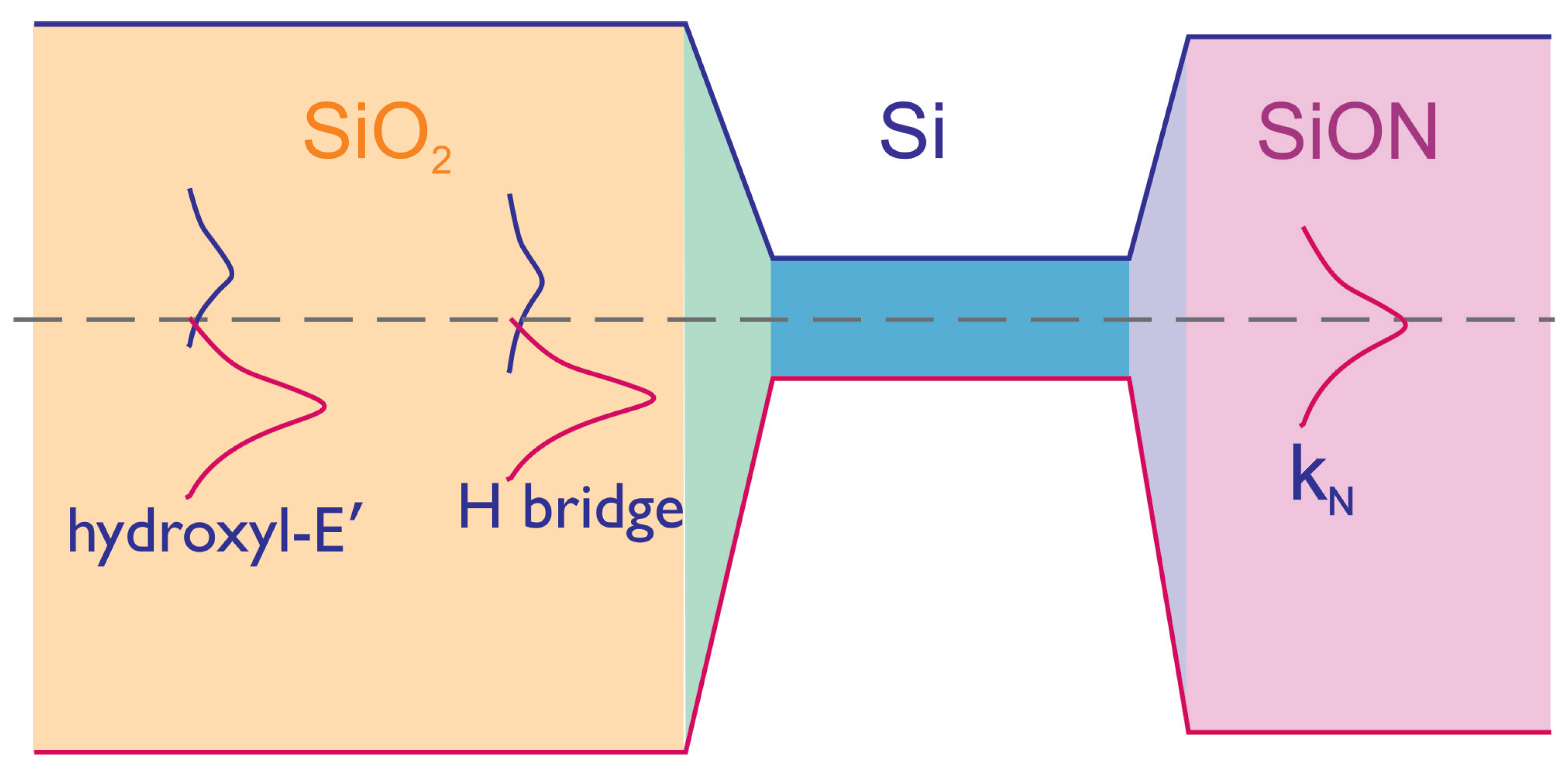
4.3. Interpretation of the Results

According to the current understanding of the microscopic nature of BTI in SiO 2 -based transistors, traps responsible for this detrimental phenomenon are the hydrogen bridges and the hydroxyl-E’ centers [63]. These traps form two bands in the band gap of SiO 2 : the band of acceptor-like states, which is situated in the upper half of the band gap, and the band of donor-like states in the lower half of the band gap [62,64]; see Figure 23. The centroid of the band of donor-like traps is situated below the Si valence band edge; therefore, the charge exchange between these traps and the valence band results in NBTI (and its recovery). On the other hand, the energetical levels of acceptor-like traps are close to the conduction band of Si, but their density-of-states is low; therefore, they provide a negligible contribution to PBTI (this behavior is consistent with experimental data reported in this work). As for traps responsible for BTI in SiON/Si 3 N 4 -based MOSFETs, they were identified as k N centers with the corresponding trap density-of-states featuring a peak close to the center of the Si band gap [64,65,66,67]. As a result, they are more easily accessible for holes, thereby making the NBTI stronger in MOSFETs with SiON/Si 3 N 4 layers compared to their SiO 2 -based counterparts (under the same stress conditions). Therefore, an increasing N content in the SiON film leads to the “transition” from the hydrogen bridges and hydroxyl-E’ centers to k N centers and hence more prominent NBTI. This picture is consistent with the explanation of stronger NBTI typical for SiON-based devices compared to MOSFETs with SiO 2 as the gate dielectric given by Reisinger et al. [35,68].
As for HBD, this event is a terminal stage of TDDB when a local concentration of generated defects is so high that these defects form a percolation path (with ohmic conductivity) [12,50]. Recent studies suggested that the microscopic mechanism underlying defect creation during TDDB/HBD is generation of O vacancies driven by the double trapping of electrons at wide angle O-Si-O sites (defect precursors) [69,70]. Although we are not aware of any papers studying the structure of TDDB-related defects and their precursors at a varying concentration of N in SiON, we can speculate that, at a higher N concentration, the energetical position of defect precursors becomes more favorable for phonon-assisted tunneling, thereby giving rise to defect creation and thus HBD at lower fields/voltages.

5. Conclusions

We compared bias temperature instability and hard breakdown characteristics of planar transistors with SiON layers with different nitrogen content. To accomplish this task, we attracted MOSFETs fabricated using processes with 1000 W (POR) and 900 W (SN) powers of radio frequency plasma nitridation; consequently, corresponding SiON films were exposed to different doses of N. In addition to this, we also used samples which—although fabricated by the same process flow—have different targeted thicknesses of SiON layers, thereby leading to different values of the N content. Nitrogen incorporated in gate oxides is known to result in positive charges distributed throughout the dielectric layer; these charges result in a threshold voltage shift towards lower V t values. The threshold voltages values of pristine devices are consistent with the N content estimated based on the process flow details.
All MOSFETs were subjected to ramped voltage stress to study the BTI and HBD behavior of these transistors. In case of BTI, p-channel MOSFETs were stressed in the NBTI regime and nMOSFETs were subjected to PBTI. Regarding HBD, stress measurements applied to n- and p-channel MOSFETs were carried out at positive and negative gate voltages, respectively.
NBTI data demonstrated a pronounced trend—NBTI reliability is correlated with the N concentration of SiON layers, i.e., devices with a lower N content demonstrated a superior NBTI behavior (smaller Δ V t shifts and longer TTF values). PBTI appeared to be negligibly weak in both devices with low and high N content. In the case of HBD, we compared MOSFETs with the same targeted thickness of SiON layers but fabricated using POR and SN processes. The latter samples have a lower N concentration; their Weibull distribution of the breakdown electric field is shifted towards higher values with respect to that obtained for MOSFETs with a high N content. Therefore, similar to BTI, transistors with a smaller N concentration feature a superior HBD behavior.
The aggravation of BTI in MOSFETs with a higher N concentration can be explained within the paradigm that in SiO 2 -based (or SiON with a low N dose) transistors, traps responsible for BTI are the hydrogen bridges and hydroxyl-E’ centers, while in transistors with SiON/Si 3 N 4 as the gate dielectric, BTI originates from k N centers, which have different energy positions and therefore are more accessible by carriers. Regarding HBD, this event corresponds to such a high concentration of traps, that they form a percolation path and the dielectric film loses its insulating properties. The physical mechanism underlying the defect creation is related to double electron trapping at a wide angle O-Si-O bond, and we expect that at a higher N concentration, energetical positions of these precursor sites are shifted towards values more favorable for tunneling.
It is worth emphasizing that there is no consensus in literature regarding the impact of nitridation on BTI behavior; therefore, our result is consistent with findings of those groups who reported aggravation of BTI in strongly nitrided SiON films. Regarding the influence of nitridation on HBD, there are the very limited number of papers dealing with this topic; our contribution additionally confirms that HBD occurs at lower electric fields in devices with a higher N content.

Author Contributions

Conceptualization, all; methodology, all; software, B.O., S.T. and A.C.; validation, S.T. and B.O.; formal analysis, S.T., B.O., Y.R., T.C., C.T.d.C.C., Y.K., R.R. and J.M.; investigation, all; resources, A.C., S.V.P. and J.R.; data curation, S.T., B.O. and A.C.; writing—original draft preparation, S.T.; writing—review and editing, all; visualization, S.T. and B.O.; supervision, S.V.P., J.R. and B.K.; project administration, A.C., S.V.P. and J.R.; funding acquisition, S.V.P. and J.R. All authors have read and agreed to the published version of the manuscript.

Funding

This research received no external funding.

Data Availability Statement

The data presented in this study are available on request from the corresponding author.

Conflicts of Interest

The authors declare no conflict of interest.

Abbreviations

The following abbreviations are used in this manuscript:
BTIBias temperature Instability
CVS        Constant Voltage Stress
eMSMextended Measure–Stress–Measure (technique)
EOLEquivalent Oxide Thickness
HBDHard Breakdown
HCDHot-Carrier Degradation
MOSFETMetal–Oxide–Semiconductor Field Effect Transistor
NBTINegative Bias Temperature Instability
PBTIPositive Bias Temperature Instability
PORProcess of Reference
RFRadio Frequency
RVSRamped Voltage Stress
SNSoft Nitridation
TDDBTime-Dependent Dielectric Breakdown

References

  1. Auth, C.; Allen, C.; Blattner, A.; Bergstrom, D.; Brazier, M.; Bost, M.; Buehler, M.; Chikarmane, V.; Ghani, T.; Glassman, T.; et al. A 22 nm high performance and low-power CMOS technology featuring fully-depleted tri-gate transistors, self-aligned contacts and high density MIM capacitors. In Proceedings of the 2012 Symposium on VLSI Technology (VLSIT), Honolulu, HI, USA, 12–14 June 2012; pp. 131–132. [Google Scholar] [CrossRef]
  2. Ferain, I.; Colinge, C.; Colinge, J.-P. Multigate transistors as the future of classical metal-oxide-semiconductor field-effect transistors. Nature 2011, 479, 310–316. [Google Scholar] [CrossRef] [PubMed]
  3. Barraud, S.; Lapras, V.; Previtali, B.; Samson, M.P.; Lacord, J.; Martinie, S.; Jaud, M.A.; Athanasiou, S.; Triozon, F.; Rozeau, O.; et al. Performance and design considerations for gate-all-around stacked-NanoWires FETs. In Proceedings of the 2017 IEEE International Electron Devices Meeting (IEDM), San Francisco, CA, USA, 2–6 December 2017; pp. 29.2.1–29.2.4. [Google Scholar] [CrossRef] [Green Version]
  4. Nagy, D.; Espiñeira, G.; Indalecio, G.; García-Loureiro, A.J.; Kalna, K.; Seoane, N. Benchmarking of FinFET, Nanosheet, and Nanowire FET Architectures for Future Technology Nodes. IEEE Access 2020, 8, 53196–53202. [Google Scholar] [CrossRef]
  5. Weckx, P.; Ryckaert, J.; Putcha, V.; De Keersgieter, A.; Boemmels, J.; Schuddinck, P.; Jang, D.; Yakimets, D.; Bardon, M.G.; Ragnarsson, L.Å.; et al. Stacked nanosheet fork architecture for SRAM design and device co-optimization toward 3 nm. In Proceedings of the 2017 IEEE International Electron Devices Meeting (IEDM), San Francisco, CA, USA, 2–6 December 2017; pp. 20.5.1–20.5.4. [Google Scholar] [CrossRef]
  6. Zhang, J.; Frougier, J.; Greene, A.; Miao, X.; Yu, L.; Vega, R.; Montanini, P.; Durfee, C.; Gaul, A.; Pancharatnam, S.; et al. Full Bottom Dielectric Isolation to Enable Stacked Nanosheet Transistor for Low Power and High Performance Applications. In Proceedings of the 2019 IEEE International Electron Devices Meeting (IEDM), San Francisco, CA, USA, 7–11 December 2019; pp. 11.6.1–11.6.4. [Google Scholar] [CrossRef]
  7. Ritzenthaler, R.; Mertens, H.; Eneman, G.; Simoen, E.; Bury, E.; Eyben, P.; Bufler, F.M.; Oniki, Y.; Briggs, B.; Chan, B.; et al. Comparison of Electrical Performance of Co-Integrated Forksheets and Nanosheets Transistors for the 2 nm Technological Node and Beyond. In Proceedings of the 2021 IEEE International Electron Devices Meeting (IEDM), San Francisco, CA, USA, 11–16 December 2021; pp. 26.2.1–26.2.4. [Google Scholar] [CrossRef]
  8. Ryckaert, J.; Schuddinck, P.; Weckx, P.; Bouche, G.; Vincent, B.; Smith, J.; Sherazi, Y.; Mallik, A.; Mertens, H.; Demuynck, S.; et al. The Complementary FET (CFET) for CMOS scaling beyond N3. In Proceedings of the 2018 IEEE Symposium on VLSI Technology, Honolulu, HI, USA, 18–22 June 2018; pp. 141–142. [Google Scholar] [CrossRef]
  9. Liebmann, L.; Smith, J.; Chanemougame, D.; Gutwin, P. CFET Design Options, Challenges, and Opportunities for 3D Integration. In Proceedings of the 2021 IEEE International Electron Devices Meeting (IEDM), San Francisco, CA, USA, 11–16 December 2021; pp. 3.1.1–3.1.4. [Google Scholar] [CrossRef]
  10. Huard, V.; Denais, M.; Parthasarathy, C. NBTI Degradation: From Physical Mechanisms to Modelling. Microel. Reliab. 2006, 46, 1–23. [Google Scholar] [CrossRef]
  11. Grasser, T.; Kaczer, B.; Gös, W.; Reisinger, H.; Aichinger, T.; Hehenberger, P.; Wagner, P.J.; Franco, J.; Toledano-Luque, M.; Nelhiebel, M. The Paradigm Shift in Understanding the Bias Temperature Instability: From Reaction-Diffusion to Switching Oxide Traps. IEEE Trans. Electron. Dev. 2011, 58, 3652–3666. [Google Scholar] [CrossRef]
  12. Degraeve, R.; Groeseneken, G.; Bellens, R.; Ogier, J.L.; Depas, M.; Roussel, P.J.; Maes, H.E. New insights in the relation between electron trap generation and the statistical properties of oxide breakdown. IEEE Trans. Electron. Dev. 1998, 45, 904–911. [Google Scholar] [CrossRef]
  13. McPherson, J.W.; Khamankar, R.B. Molecular model for intrinsic time-dependent dielectric breakdown in SiO 2 dielectrics and the reliability implications for hyper-thin gate oxide. Semicond. Sci. Technol. 2000, 15, 462. [Google Scholar] [CrossRef]
  14. Rauch, S.; Rosa, G.L. CMOS Hot Carrier: From Physics to End of Life Projections, and Qualification. In Proceedings of the International Reliability Physics Symposium (IRPS), Garden Grove (Anaheim), CA, USA, 2–6 May 2010. [Google Scholar]
  15. Bravaix, A.; Huard, V. Hot-Carrier Degradation Issues in Advanced CMOS Nodes. In Proceedings of the European Symposium on Reliability of Electron Devices Failure Physics and Analysis (ESREF), Gaeta, Italy, 11–15 October 2010; pp. 1267–1272. [Google Scholar]
  16. Tyaginov, S.; Grasser, T. Modeling of hot-carrier degradation: Physics and controversial issues. In Proceedings of the 2012 IEEE International Integrated Reliability Workshop Final Report, South Lake Tahoe, CA, USA, 14–18 October 2012; pp. 206–215. [Google Scholar] [CrossRef]
  17. Ramey, S.; Ashutosh, A.; Auth, C.; Clifford, J.; Hattendorf, M.; Hicks, J.; James, R.; Rahman, A.; Sharma, V.; Amour, A.S.; et al. Intrinsic transistor reliability improvements from 22 nm tri-gate technology. In Proceedings of the 2013 IEEE International Reliability Physics Symposium (IRPS), Monterey, CA, USA, 14–18 April 2013; pp. 4C.5.1–4C.5.5. [Google Scholar] [CrossRef]
  18. Rahman, A.; Dacuna, J.; Nayak, P.; Leatherman, G.; Ramey, S. Reliability Studies of a 10 nm High-performance and Low-power CMOS Technology Featuring 3rd Generation FinFET and 5th Generation HK/MG. In Proceedings of the 2018 IEEE International Reliability Physics Symposium (IRPS), Burlingame, CA, USA, 11–15 March 2018; pp. 6F.4-1–6F.4-6. [Google Scholar] [CrossRef]
  19. Bravaix, A.; Guerin, C.; Huard, V.; Roy, D.; Roux, J.; Vincent, E. Hot-carrier Acceleration Factors for Low Power Management in DC-AC Stressed 40 nm NMOS Node at High Temperature. In Proceedings of the International Reliability Physics Symposium (IRPS), Montreal, QC, Canada, 26–30 April 2009; pp. 531–546. [Google Scholar] [CrossRef]
  20. Guerin, C.; Huard, V.; Bravaix, A. General Framework about Defect Creation at the Si/SiO2 Interface. J. Appl. Phys. 2009, 105, 114513-1–114513-12. [Google Scholar] [CrossRef]
  21. Tyaginov, S.; Starkov, I.; Triebl, O.; Cervenka, J.; Jungemann, C.; Carniello, S.; Park, J.; Enichlmail, H.; Kernstock, C.; Seebacher, E.; et al. Interface Traps Density-of-states as a Vital Component for Hot-carrier Degradation Modeling. Microelectron. Reliab. 2010, 50, 1267–1272. [Google Scholar] [CrossRef]
  22. Tyaginov, S.; Starkov, I.; Jungemann, C.; Enichlmair, H.; Park, J.; Grasser, T. Impact of the Carrier Distribution Function on Hot-Carrier Degradation Modeling. In Proceedings of the European Solid-State Device Research Conference (ESSDERC), Helsinki, Finland, 12–16 September 2011; pp. 151–154. [Google Scholar] [CrossRef]
  23. Tallarico, A.; Reggiani, S.; Magnone, P.; Croce, G.; Depetro, R.; Gattari, P.; Sangiorgi, E.; Fiegna, C. Investigation of the hot carrier degradation in power LDMOS transistors with customized thick oxide. Microelectron. Reliab. 2017, 76–77, 475–479. [Google Scholar] [CrossRef] [Green Version]
  24. Tallarico, A.N.; Reggiani, S.; Depetro, R.; Torti, A.M.; Croce, G.; Sangiorgi, E.; Fiegna, C. Hot-Carrier Degradation in Power LDMOS: Selective LOCOS- Versus STI-Based Architecture. IEEE J. Electron Devices Soc. 2018, 6, 219–226. [Google Scholar] [CrossRef]
  25. Joo, M.S.; Yeo, I.S.; Lee, C.H.; Cho, H.J.; Jang, S.A.; Lee, S.K. Effects of nitridation pressure on the characteristics of gate dielectrics annealed in N2O ambient. IEEE Electron Device Lett. 1999, 20, 445–447. [Google Scholar] [CrossRef]
  26. Mazumder, M.; Teramoto, A.; Komori, J.; Sekine, M.; Kawazu, S.; Mashiko, Y. Effects of N distribution on charge trapping and TDDB characteristics of N/sub 2/O annealed wet oxide. IEEE Trans. Electron Dev. 1999, 46, 1121–1126. [Google Scholar] [CrossRef]
  27. Chen, Y.; Chien, C.; Lou, J. Dielectric properties of nitric oxide-annealed gate oxides grown on nitrogen-implanted silicon substrates. Thin Solid Films 2006, 513, 264–268. [Google Scholar] [CrossRef]
  28. Lee, H.; Pilkington, S.J.; Knebel, S.; Voon, H.C.; Loi, C.M.; Ong, M.I.I. The effects of Fluorine implantation and ex-situ Nitrogen anneal on Reliability improvement of 5 V CMOSFETs. In Proceedings of the 2022 IEEE International Conference on Semiconductor Electronics (ICSE), Kuala Lumpur, Malaysia, 15–17 August 2022; pp. 41–44. [Google Scholar] [CrossRef]
  29. O’Sullivan, B.J.; Ritzenthaler, R.; Dentoni Litta, E.; Simoen, E.; Machkaoutsan, V.; Fazan, P.; Ji, Y.H.; Kim, C.; Spessot, A.; Linten, D.; et al. Overview of Bias Temperature Instability in Scaled DRAM Logic for Memory Transistors. IEEE Trans. Dev. Mater. Reliab. 2020, 20, 258–268. [Google Scholar] [CrossRef]
  30. O’Connor, R.; Aoulaiche, M.; Pantisano, L.; Shickova, A.; Degraeve, R.; Kaczer, B.; Groeseneken, G. The role of nitrogen in HfSiON defect passivation. In Proceedings of the 2009 IEEE International Reliability Physics Symposium, Montreal, QC, Canada, 26–30 April 2009; pp. 921–924. [Google Scholar] [CrossRef]
  31. Maheta, V.D.; Olsen, C.; Ahmed, K.; Mahapatra, S. The Impact of Nitrogen Engineering in Silicon Oxynitride Gate Dielectric on Negative-Bias Temperature Instability of p-MOSFETs: A Study by Ultrafast On-The-Fly IDLIN Technique. IEEE Trans. Electron Dev. 2008, 55, 1630–1638. [Google Scholar] [CrossRef]
  32. Joshi, K.; Hung, S.; Mukhopadhyay, S.; Chaudhary, V.; Nanaware, N.; Rajamohnan, B.; Sato, T.; Bevan, M.; Wei, A.; Noori, A.; et al. HKMG process impact on N, P BTI: Role of thermal IL scaling, IL/HK integration and post HK nitridation. In Proceedings of the 2013 IEEE International Reliability Physics Symposium (IRPS), Monterey, CA, USA, 14–18 April 2013; pp. 4C.2.1–4C.2.10. [Google Scholar] [CrossRef]
  33. Garros, X.; Casse, M.; Reimbold, G.; Martin, F.; Leroux, C.; Fanton, A.; Renault, O.; Cosnier, V.; Boulanger, F. Guidelines to improve mobility performances and BTI reliability of advanced high-k/metal gate stacks. In Proceedings of the 2008 Symposium on VLSI Technology, Honolulu, HI, USA, 17–19 June 2008; pp. 68–69. [Google Scholar] [CrossRef]
  34. Garros, X.; Casse, M.; Fenouillet-Beranger, C.; Reimbold, G.; Martin, F.; Gaumer, C.; Wiemer, C.; Perego, M.; Boulanger, F. Detrimental impact of technological processes on BTI reliability of advanced high-K/metal gate stacks. In Proceedings of the 2009 IEEE International Reliability Physics Symposium, Montreal, QC, Canada, 26–30 April 2009; pp. 362–366. [Google Scholar] [CrossRef]
  35. Reisinger, H.; Vollertsen, R.P.; Wagner, P.J.; Huttner, T.; Martin, A.; Aresu, S.; Gustin, W.; Grasser, T.; Schlunder, C. A Study of NBTI and Short-Term Threshold Hysteresis of Thin Nitrided and Thick Non-Nitrided Oxides. IEEE Trans. Dev. Mater. Reliab. 2009, 9, 106–114. [Google Scholar] [CrossRef]
  36. Takasaki, K.; Irino, K.; Aoyama, T.; Momiyama, Y.; Nakanishi, T.; Tamura, Y.; Ito, T. Impact of Nitrogen Profile in Gate Nitrided-Oxide on Deep-Submicron CMOS Performance and Reliability. Fujitsu Sci. Tech. J. 2003, 39, 40–51. [Google Scholar]
  37. Bury, E.; Chasin, A.; Kaczer, B.; Vandemaele, M.; Tyaginov, S.; Franco, J.; Ritzenthaler, R.; Mertens, H.; Weckx, P.; Horiguchi, N.; et al. Evaluating Forksheet FET Reliability Concerns by Experimental Comparison with Co-integrated Nanosheets. In Proceedings of the 2022 IEEE International Reliability Physics Symposium (IRPS), Dallas, TX, USA, 27–31 March 2022; pp. 5A.2–1–5A.2–7. [Google Scholar] [CrossRef]
  38. Vandemaele, M.; Kaczer, B.; Tyaginov, S.; Franco, J.; Bury, E.; Chasin, A.; Makarov, A.; Hellings, G.; Groeseneken, G. Trapping of Hot Carriers in the Forksheet FET Wall: A TCAD Study. IEEE Electron Dev. Lett. 2023, 44, 197–200. [Google Scholar] [CrossRef]
  39. Hauser, J.R.; Ahmed, K. Characterization of ultra-thin oxides using electrical C-V and I-V measurements. AIP Conf. Proc. 1998, 449, 235–239. [Google Scholar] [CrossRef]
  40. Kaczer, B.; Franco, J.; Weckx, P.; Roussel, P.J.; Bury, E.; Cho, M.; Degraeve, R.; Linten, D.; Groeseneken, G.; Kukner, H.; et al. The defect-centric perspective of device and circuit reliability—From individual defects to circuits. In Proceedings of the 2015 45th European Solid State Device Research Conference (ESSDERC), Graz, Austria, 14–18 September 2015; pp. 218–225. [Google Scholar]
  41. Asenov, A. Random Dopant Induced Threshold Voltage Lowering and Fluctuations in sub-0.1 μm MOSFET’s: A 3-D Atomistic Simulation Study. IEEE Trans. Electron. Dev. 1998, 45, 2505–2513. [Google Scholar] [CrossRef] [Green Version]
  42. Brown, A.R.; Watling, J.R.; Asenov, A.; Bersuker, G.; Zeitzoff, P. Intrinsic Parameter Fluctuations in MOSFETs due to Structural Non-uniformity of High-κ Gate Stack Materials. In Proceedings of the 2005 International Conference On Simulation of Semiconductor Processes and Devices, Tokyo, Japan, 1–3 September 2005; pp. 27–30. [Google Scholar] [CrossRef]
  43. Brown, A.R.; Watling, J.R.; Asenov, A. Intrinsic Parameter Fluctuations due to Random Grain Orientations in High-κ Gate Stacks. J. Comput. Electron. 2006, 5, 333–336. [Google Scholar] [CrossRef]
  44. Asenov, A.; Kaya, S.; Davies, J.H. Intrinsic Threshold Voltage fluctuations in Decanano MOSFETs due to Local Oxide Thickness Variations. IEEE Trans. Electron. Dev. 2002, 49, 112–119. [Google Scholar] [CrossRef] [Green Version]
  45. Tyaginov, S.; Vexler, M.; Shulekin, A.; Grekhov, I. Statistical Analysis of Tunnel Currents in Scaled MOS Structures with a Non-uniform Oxide Thickness Distribution. Solid-State Electron. 2005, 49, 1192–1197. [Google Scholar] [CrossRef]
  46. Rawat, A.; Harsha Vardhan, P.; Ganguly, U. Nanoscale Transistor Variability Modeling: How Simple Physics Enables a Powerful Prediction Platform. IEEE Nanotechnol. Mag. 2020, 14, 4–16. [Google Scholar] [CrossRef]
  47. Grasser, T.; Reisinger, H.; Wagner, P.J.; Schanovsky, F.; Goes, W.; Kaczer, B. The Time Dependent Defect Spectroscopy (TDDS) for the Characterization of the Bias Temperature Instability. In Proceedings of the 2010 IEEE International Reliability Physics Symposium, Anaheim, CA, USA, 2–6 May 2010; pp. 16–25. [Google Scholar] [CrossRef]
  48. Kaczer, B.; Franco, J.; Cho, M.; Grasser, T.; Roussel, P.J.; Tyaginov, S.; Bina, M.; Wimmer, Y.; Procel, L.M.; Trojman, L.; et al. Origins and Implications of Increased Channel hot Carrier Variability in nFinFETs. In Proceedings of the 2015 IEEE International Reliability Physics Symposium, Monterey, CA, USA, 19–23 April 2015; pp. 3B.5.1–3B.5.6. [Google Scholar] [CrossRef] [Green Version]
  49. Makarov, A.; Kaczer, B.; Chasin, A.; Vandemaele, M.; Bury, E.; Jech, M.; Grill, A.; Hellings, G.; El-Sayed, A.; Grasser, T.; et al. Bi-Modal Variability of nFinFET Characteristics During Hot-Carrier Stress: A Modeling Approach. IEEE Electron Dev. Lett. 2019, 40, 1579–1582. [Google Scholar] [CrossRef]
  50. Monsieur, F.; Vincent, E.; Ribes, G.; Huard, V.; Bruyere, S.; Roy, D.; Pananakakis, G.; Ghibaudo, G. Evidence for defect-generation-driven wear-out of breakdown conduction path in ultra thin oxides. In Proceedings of the International Reliability Physics Symposium (IRPS), Dallas, TX, USA, 30 March–4 April 2003; pp. 424–431. [Google Scholar] [CrossRef]
  51. Kerber, A.; Cartier, E.A. Reliability Challenges for CMOS Technology Qualifications with Hafnium Oxide/Titanium Nitride Gate Stacks. IEEE Trans. Dev. Mater. Reliab. 2009, 9, 147–162. [Google Scholar] [CrossRef]
  52. Kerber, A.; Krishnan, S.A.; Cartier, E.A. Voltage Ramp Stress for Bias Temperature Instability Testing of Metal-Gate/High- k Stacks. IEEE Electron Dev. Lett. 2009, 30, 1347–1349. [Google Scholar] [CrossRef]
  53. Kaczer, B.; Grasser, T.; Roussel, P.; Martin-Martinez, J.; O’Conner, R.; O’Sillivan, B.; Groeseneken, G. Ubiquitous Relaxation in BTI Stressing New Evaluation and Insights. In Proceedings of the 46th Annual International Reliability Physics Symposium, Phoenix, AZ, USA, 27 April–1 May 2008; pp. 20–27. [Google Scholar] [CrossRef]
  54. Degraeve, R.; Groeseneken, G.; Bellens, R.; Depas, M.; Maes, H.E. A consistent model for the thickness dependence of intrinsic breakdown in ultra-thin oxides. In Proceedings of the International Electron Devices Meeting, Washington, DC, USA, 10–13 December 1995; pp. 863–866. [Google Scholar] [CrossRef]
  55. Monsieur, F.; Vincent, E.; Pananakakis, G.; Ghibaudo, G. Wear-out, breakdown occurrence and failure detection in 18–25 A ultrathin oxides. Microelectron. Reliab. 2001, 41, 1035–1039. [Google Scholar] [CrossRef]
  56. Monsieur, F.; Vincent, E.; Roy, D.; Bruyere, S.; Vildeuil, J.; Pananakakis, G.; Ghibaudo, G. A Thorough Investigation of Progressive Breakdown in Ultra-thin Oxides. Physical Understanding and Application for Industrial Reliability Assessment. In Proceedings of the International Reliability Physics Symposium (IRPS), Dallas, TX, USA, 7–11 April 2002; pp. 45–54. [Google Scholar] [CrossRef]
  57. Kim, A.; Wu, E.; Li, B.; Linder, B. Transformation of Ramped Current Stress VBDto Constant Voltage Stress TDDB TBD. In Proceedings of the 2019 IEEE International Reliability Physics Symposium (IRPS), Monterey, CA, USA, 31 March–4 April 2019; pp. 1–5. [Google Scholar] [CrossRef]
  58. Benard, A. Het Uitzetten van Waarneningen op Waarschijunlijkdeid Papier (The Plotting of Observations or Probability Paper). Stat. Neerl. 1953, 7, 163–173. [Google Scholar] [CrossRef] [Green Version]
  59. Cartier, E.; DiMaria, D. Hot-Electron Dynamics in SiO2 and the Degradation of the Si/SiO2-interface. Microelectron. Eng. 1993, 22, 207–210. [Google Scholar] [CrossRef]
  60. DiMaria, D.J.; Cartier, E.; Arnold, D. Impact ionization, trap creation, degradation, and breakdown in silicon dioxide films on silicon. J. Appl. Phys. 1993, 73, 3367–3384. [Google Scholar] [CrossRef]
  61. Bastos, J.P.; O’Sullivan, B.J.; Franco, J.; Tyaginov, S.; Truijen, B.; Chasin, A.; Degraeve, R.; Kaczer, B.; Ritzenthaler, R.; Capogreco, E.; et al. Bias Temperature Instability (BTI) of High-Voltage Devices for Memory Periphery. In Proceedings of the 2022 IEEE International Reliability Physics Symposium (IRPS), Dallas, TX, USA, 27–31 March 2022; pp. 1–6. [Google Scholar] [CrossRef]
  62. Rzepa, G.; Franco, J.; O’Sullivan, B.; Subirats, A.; Simicic, M.; Hellings, G.; Weckx, P.; Jech, M.; Knobloch, T.; Waltl, M.; et al. Comphy—A compact-physics framework for unified modeling of BTI. Microelectron. Reliab. 2018, 85, 49–65. [Google Scholar] [CrossRef]
  63. Wimmer, Y.; El-Sayed, A.M.; Gös, W.; Grasser, T.; Shluger, A.L. Role of Hydrogen in Volatile Behaviour of Defects in SiO2-Based Electronic Devices. Proc. R. Soc. Lond. A Math. Phys. Eng. Sci. 2016, 472, 20160009. [Google Scholar] [CrossRef]
  64. Michl, J. Charge Trapping and Variability in CMOS Technologies at Cryogenic Temperatures. Ph.D. Thesis, University of Vienna, Wien, Austria, 2022. [Google Scholar]
  65. Campbell, J.; Lenahan, P.; Krishnan, A.; Krishnan, S. NBTI: An Atomic-Scale Defect Perspective. In Proceedings of the International Reliability Physics Symposium (IRPS), San Jose, CA, USA, 26–30 March 2006; pp. 442–447. [Google Scholar] [CrossRef]
  66. Campbell, J.P.; Lenahan, P.M.; Krishnan, A.T.; Krishnan, S. Identification of atomic-scale defect structure involved in the negative bias temperature instability in plasma-nitrided devices. Appl. Phys. Lett. 2007, 91, 133507. [Google Scholar] [CrossRef]
  67. Campbell, J.; Lenahan, P.; Krishnan, A.; Krishnan, S. Location, Structure, and Density of States of NBTI-Induced Defects in Plasma Nitrided pMOSFETs. In Proceedings of the 2007 IEEE International Reliability Physics Symposium Proceedings. 45th Annual, Phoenix, AZ, USA, 15–19 April 2007; pp. 503–510. [Google Scholar] [CrossRef]
  68. Reisinger, H.; Grasser, T.; Hofmann, K.; Gustin, W.; Schlünder, C. The impact of recovery on BTI reliability assessments. In Proceedings of the 2010 IEEE International Integrated Reliability Workshop Final Report, South Lake Tahoe, CA, USA, 17–21 October 2010; pp. 12–16. [Google Scholar] [CrossRef]
  69. Padovani, A.; Gao, D.Z.; Shluger, A.L.; Larcher, L. A Microscopic Mechanism of Dielectric Breakdown in SiO2 Films: An Insight from Multi-scale Modeling. J. Appl. Phys. 2017, 121, 155101. [Google Scholar] [CrossRef] [Green Version]
  70. Padovani, A.; Torraca, P.L.; Strand, J.; Shluger, A.; Milo, V.; Larcher, L. Towards a Universal Model of Dielectric Breakdown. In Proceedings of the 2023 IEEE International Reliability Physics Symposium (IRPS), Monterey, CA, USA, 26–30 March 2023; pp. 1–8. [Google Scholar] [CrossRef]
Figure 1. Schematic representation of RVS BTI measurements.
Micromachines 14 01514 g001
Figure 2. Schematic representation of the Δ V t extraction technique. First, the I d V g curve of the pristine device is measured, thereby allowing the extraction of V t and I t . Next, at each stress time step t, V t ( t ) is determined as the gate voltage at which I d ( V g ) = I t and therefore Δ V t ( t ) = V t ( t ) V t ( 0 ) .
Micromachines 14 01514 g002
Figure 3. The typical evolution of the source-drain current I s during RVS NBTI stress. These current values were measured during sense phases. One can observe that I s decreases with the stress voltage; this decrease is a manifestation of device degradation during NBTI. At a lower ramp rate, the I s change is more pronounced. The data are shown for the SN pMOSFET with the targeted physical thickness of 1.9 nm (S #2).
Micromachines 14 01514 g003
Figure 4. S #1 (POR), pMOSFETs: the threshold voltage shift Δ V t caused by NBTI in pMOSFETs as a function of the overdrive oxide field E ov . The experimental Δ V t ( E ov ) dependency is reproduced by Equation (1).
Micromachines 14 01514 g004
Figure 5. The same as Figure 4 but for S #2 (SN).
Micromachines 14 01514 g005
Figure 6. The same as Figure 4 but for S #3 (POR + 2 Å).
Micromachines 14 01514 g006
Figure 7. The same as Figure 4 but for S #4 (SN − 2 Å).
Micromachines 14 01514 g007
Figure 8. The same as Figure 4 but for S #5 (SN − 2 Å).
Micromachines 14 01514 g008
Figure 9. S #1 (POR), pMOSFETs: device time-to-failure (corresponding to the threshold voltage shift of Δ V t = 30 mV) as a function of the overdrive voltage V ov . The upper limit of the safe operating area is determined as the V ov corresponding to TTF of 10 years.
Micromachines 14 01514 g009
Figure 10. The same as Figure 4 but for S #2 (SN).
Micromachines 14 01514 g010
Figure 11. The same as Figure 4 but for S #3 (POR + 2 Å).
Micromachines 14 01514 g011
Figure 12. The same as Figure 4 but for S #4 (SN − 2 Å).
Micromachines 14 01514 g012
Figure 13. The same as Figure 5 but for S #5 (SN − 2 Å).
Micromachines 14 01514 g013
Figure 14. Δ V t ( E ov ) dependencies measured during PBTI stress applied to the MOSFET which was fabricated by the POR process and has the targeted SiON thickness of 1.9 nm (S #1). One can observe that at the highest E ov value of 20 MV/cm, the threshold voltage shift hardly reaches 4 mV; therefore, we can conclude that PBTI is negligibly weak. The same holds true for all other devices studied in this work (data sets for other devices are not shown in the paper).
Micromachines 14 01514 g014
Figure 15. Gate current I g as a function of stress voltage V g recorded during RVS HBD measurements conducted on the POR nMOSFET with the targeted SiON thickness of 1.9 nm (sample S #1).
Micromachines 14 01514 g015
Figure 16. The same as Figure 15, but for the nMOSFET which received softer nitridation with the targeted SiON thickness of 1.9 nm (sample S #2).
Micromachines 14 01514 g016
Figure 17. Weibit plots of breakdown voltages for the nMOSFETs fabricated by the POR (S #1, red symbols) and those exposed to SN (S #2, green symbols).
Micromachines 14 01514 g017
Figure 18. Weibit plots for breakdown fields extracted for nMOSFETs grown by POR and SN processes.
Micromachines 14 01514 g018
Figure 19. S #1 (POR), pMOSFETs: gate current I g as a function of stress voltage V g recorded during RVS HBD measurements conducted on the POR nMOSFET (sample S #1).
Micromachines 14 01514 g019
Figure 20. The same as Figure 19 but for S #2 (SN).
Micromachines 14 01514 g020
Figure 21. Weibit plots of breakdown voltages for the pMOSFETs fabricated by the POR (red symbols) and SN (green symbols).
Micromachines 14 01514 g021
Figure 22. Weibit plots for breakdown fields extracted for pMOSFETs grown by POR and SN processes.
Micromachines 14 01514 g022
Figure 23. Schematically represented charge transition levels of traps responsible for NBTI in SiO 2 -based MOSFETs—hydroxyl-E’ centers and H bridges. Both form acceptor-like states close to the edge of the Si conduction band as well as donor-like states placed below the valence band of Si. In FETs with SiON/Si 3 N 4 layers, another type of defects, namely k N centers, govern BTI. They form the defect band with a centroid close to the mid-gap of Si.
Micromachines 14 01514 g023
Table 1. Equivalent oxide thickness and threshold voltage values of samples used for BTI and HBD studies shown for n- and p-channel MOSFETs. EOT data are acquired using capacitance-voltage measurements, while for V t extraction, the maximum transconductance method (at the drain voltage V d of +0.05 and −0.05 V for n- and pMOSFETs, respectively) was employed. The last column shows the N content rank. A higher rank corresponds to a higher concentration, i.e., ‘1’ corresponds to the lowest N content and ‘4’ to the highest N concentration.
SampleDetailsEOT, nMOSEOT, pMOS V t , nMOS V t , pMOSN Content Rank
S #1POR1.48 nm1.37 nm0.23 V−0.22 V3
S #2SN1.54 nm1.48 nm0.28 V−0.17 V1
S #3POR + 2 Å1.78 nm1.66 nm0.29 V−0.20 V2
S #4SN − 2 Å1.49 nm1.34 nm0.13 V−0.27 V4
S #5SN − 2 Å1.47 nm1.28 nm0.13 V−0.27 V4
Disclaimer/Publisher’s Note: The statements, opinions and data contained in all publications are solely those of the individual author(s) and contributor(s) and not of MDPI and/or the editor(s). MDPI and/or the editor(s) disclaim responsibility for any injury to people or property resulting from any ideas, methods, instructions or products referred to in the content.

