
Reliability Study of Metal-Oxide Semiconductors in Integrated Circuits

 ,
,  ,
,
Abstract
:1. Introduction
- -
- Investigation of the possible types and causes of IC failures;
- -
- Carrying out experimental tests for failure-free operation of the microcircuit;
- -
- Analyses of the results of tests on reliability, MTBF, and electro-thermo training of ICs.
- -
- Determination of the activation energy of failure mechanisms of IMCs;
- -
- Calculation of the acceleration factor of the chip.
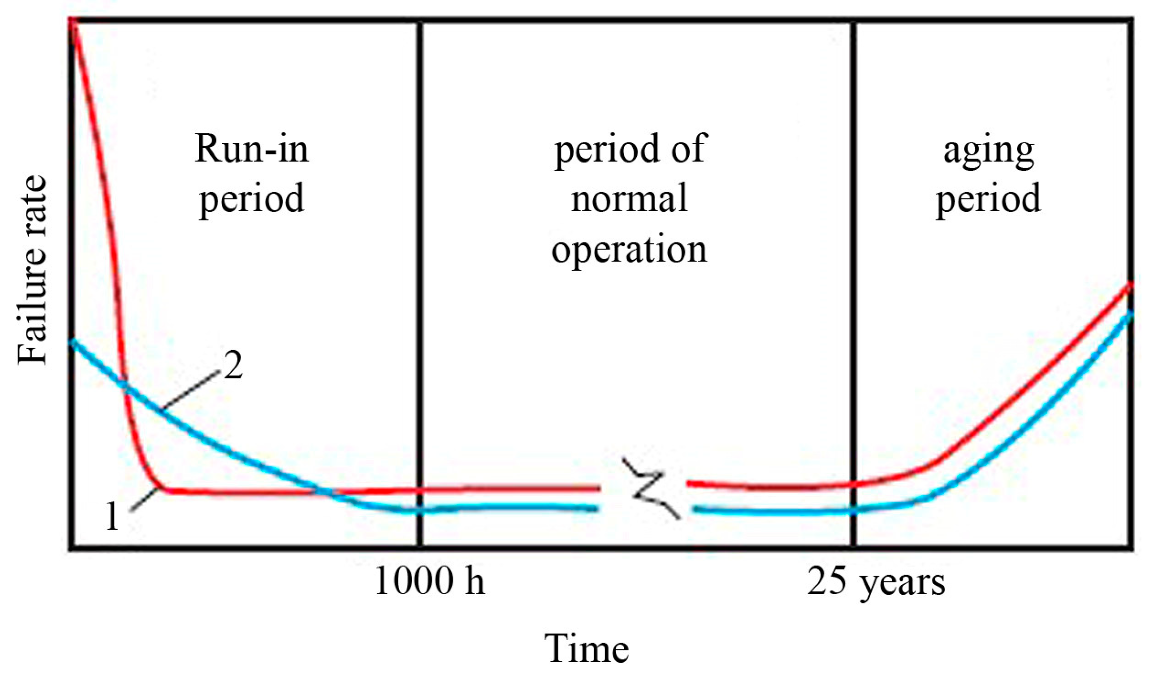
1.1. Causes of IC Failures
1.2. Technological Factors Affecting IC Failures
- -
- deviations from the specified values of oxide and polycrystalline silicon layer thicknesses;
- -
- deviations of the resistances of the implanted layers;
- -
- errors of geometrical dimensions of elements at the lithographic formation of circuit topology;
- -
- errors of phototemplate matching at different stages of the technological process.
2. Materials and Methods of Chip Reliability Testing
2.1. Description of the Object of Research
- -
- internal power supply voltage generation unit;
- -
- PWM control unit;
- -
- power key;
- -
- power key driver;
- -
- thermal protection unit;
- -
- logic control unit;
- -
- feedback control unit.
- -
- Increased life cycle of advanced special-purpose vehicles by increasing the time until failure of the developed ICs and the life expectancy;
- -
- high level of resistance to the effects of UHF;
- -
- Reduction of mass-dimension indicators of REA power supplies.
2.2. Description of Installations
- Normal conditions: 25 ± 10 °C.
- Temperature limits: −(60 ± 3), (85 ± 3) °C.
- -
- limit output current, Iout_m1;
- -
- frequency of the internal oscillator, F;
- -
- instability of the set output voltage over the entire input voltage range, Ku;
- -
- instability of the set output voltage over the whole range of load currents, KI.
2.3. Methodology of Measurements on the Measuring Bench and Calculation of Instability Coefficients of the Set Output Voltage
2.4. Test Methodology in the Heat and Cold Chamber
- -
- The temperature range in the chamber’s usable volume is 45 to 125 °C.
- -
- The error of temperature setting and maintenance, taking into account the uneven distribution in the usable volume, does not exceed ±3 °C.
- -
- Loading of the chamber with semiconductor devices is cassette.
- -
- The maximum electrical power consumed by the chamber during the mode setting period is not more than 6 kW.
- -
- The camera provides continuous operation for 10,000 h with 128 kbyte archive memory and data display on the alphanumeric display of the temperature controller.
- -
- Operating temperature of the chamber −(5 ÷ 60) °C.
- -
- Temperature maintenance accuracy ±1 °C-/in the instrument test area.
- -
- The time to reduce the chamber temperature from +20 to −60 °C is 30 min.
3. Rejection Tests
4. Failure Tests
5. Determination of the Activation Energy of IMC
6. Conclusions
Author Contributions
Funding
Institutional Review Board Statement
Informed Consent Statement
Data Availability Statement
Conflicts of Interest
References
- Wu, C. Research on reliability of complementary metal oxide semiconductor integrated circuit. Appl. Comput. Eng. 2023, 7, 8–13. [Google Scholar] [CrossRef]
- Green, M. Dummer’s Vision of Solid Circuits at the UK Royal Radar Establishment. IEEE Ann. Hist. Comput. 2013, 35, 56–66. [Google Scholar] [CrossRef]
- Groeseneken, G.; Degraeve, R.; Kaczer, B.; Roussel, P. Challenges in reliability assessment of advanced CMOS technologies. In Proceedings of the Physical and Failure Analysis of Integrated Circuits, Bangalore, India, 11–13 July 2007; pp. 1–9. [Google Scholar]
- Stathis, J.; Zafar, S. The negative bias temperature instability in MOS devices: A review. Microelectron. Reliab. 2006, 46, 270–286. [Google Scholar] [CrossRef]
- Filina, O.A.; Martyushev, N.V.; Malozyomov, B.V.; Tynchenko, V.S.; Kukartsev, V.A.; Bashmur, K.A.; Pavlov, P.P.; Panfilova, T.A. Increasing the Efficiency of Diagnostics in the Brush-Commutator Assembly of a Direct Current Electric Motor. Energies 2024, 17, 17. [Google Scholar] [CrossRef]
- Srinivasan, J. The Impact of Technology Scaling on Lifetime Reliability. In Proceedings of the International Conference on Dependable Systems and Networks, Florence, Italy, 28 June–1 July 2004; IEEE: Piscataway, NJ, USA. [Google Scholar]
- Wang, W.; Yang, S.; Bhardwaj, S.; Vattikonda, R.; Vrudhula, S.; Liu, F.; Cao, Y. The Impact of NBTI on the Performance of Combinational and Sequential Circuits. In Proceedings of the 44th Annual Design Automation Conference, San Diego, CA, USA, 4–8 June 2007. [Google Scholar]
- Martyushev, N.V.; Malozyomov, B.V.; Efremenkov, E.A.; Sorokova, S.N.; Qi, M. Mathematical Modeling of Mechanical Forces and Power Balance in Electromechanical Energy Converter. Mathematics 2023, 11, 2394. [Google Scholar] [CrossRef]
- Bhardwaj, S. Predictive Modeling of the NBTI Effect for Reliable Design. In Proceedings of the Custom Integrated Circuits Conference, 2006. CICC ’06, San Jose, CA, USA, 10–13 September 2006; IEEE: Piscataway, NJ, USA. [Google Scholar]
- Kim, S.; Kim, C.; Bong, J.H.; Hwang, W.S.; Kim, T.-S.; Oh, J.S.; Cho, B.J. Mechanical and Electrical Reliability Analysis of Flexible Si Complementary Metal-Oxide-Semiconductor Integrated Circuit. J. Nanosci. Nanotechnol. 2019, 19, 6473–6480. [Google Scholar] [CrossRef]
- Hussain, A.M.; Hussain, M.M. CMOS-technology enabled flexible and stretchable electronics for internet of everything applications. Adv. Mater. 2016, 28, 4219–4249. [Google Scholar] [CrossRef] [PubMed]
- Bong, J.H.; Kim, S.; Jeong, C.B.; Chang, K.S.; Hwang, W.S.; Cho, B.J. Reliability improvement of a flexible FD-SOI MOSFET via heat management. Appl. Phys. Lett. 2017, 110, 252101-1–252101-5. [Google Scholar] [CrossRef]
- Martyushev, N.V.; Malozyomov, B.V.; Sorokova, S.N.; Efremenkov, E.A.; Qi, M. Mathematical Modeling the Performance of an Electric Vehicle Considering Various Driving Cycles. Mathematics 2023, 11, 2586. [Google Scholar] [CrossRef]
- Maricau, E.; Gielen, G. Analog IC Reliability in Nanometer CMOS; Springer Science & Business Media: Zurich, Switzerland, 2013. [Google Scholar]
- Cao, Q.; Kim, H.; Pimparkar, N.; Kulkarni, J.P.; Wang, C.; Shim, M.; Roy, K.; Alam, M.A.; Rogers, J.A. Medium-scale carbon nanotube thin-film integrated circuits on flexible plastic substrate. Nature 2008, 454, 495–500. [Google Scholar] [CrossRef]
- Viventi, J.; Kim, D.; Vigeland, L.; Frechette, E.S.; Blanco, J.A.; Kim, Y.; Avrin, A.E.; Tiruvadi, V.R.; Hwang, S.; Vanleer, A.C.; et al. Flexible, foldable, actively multiplexed, high-density electrode array for mapping brain activity in vivo. Nat. Neurosci. 2011, 14, 1599–1605. [Google Scholar] [CrossRef]
- Semenova, E.; Tynchenko, V.; Chashchina, S.; Suetin, V.; Stashkevich, A. Using UML to Describe the Development of Software Products Using an Object Approach. In Proceedings of the 2022 IEEE International IOT, Electronics and Mechatronics Conference, IEMTRONICS 2022, Toronto, ON, Canada, 1–4 June 2022. [Google Scholar] [CrossRef]
- Huard, V.; Denais, M.; Parthasarathy, C. NBTI degradation: From physical mechanisms to modelling. Microelectron. Reliab. 2006, 46, 1–23. [Google Scholar] [CrossRef]
- Choi, S.; Lee, H.; Ghaffari, R.; Hyeon, T.; Kim, D. Recent advances in flexible and stretchable bio-electronics devices integrated with nanomaterials. Adv. Mater. 2016, 28, 4203–4218. [Google Scholar] [CrossRef] [PubMed]
- Kim, J.; Lee, M.; Shim, H.J.; Ghaffari, R.; Cho, H.R.; Son, D.; Jung, Y.H.; Soh, M.; Choi, C.; Jung, S.; et al. Stretchable silicon nanoribbon electronics for skin prosthesis. Nat. Commun. 2014, 5, 5747-1–5747-11. [Google Scholar] [CrossRef]
- Su, M.; Li, F.; Chen, S.; Huang, Z.; Qin, M.; Li, W.; Zhang, X.; Song, Y. Nanoparticle-based curve arrays for multirecognition flexible electronics. Adv. Mater. 2016, 28, 1369–1374. [Google Scholar] [CrossRef]
- Trung, T.Q.; Ramasundaram, S.; Hwang, B.; Lee, N. An all-elastomeric transparent and stretchable temperature sensor for body-attachable wearable electronics. Adv. Mater. 2016, 28, 502–509. [Google Scholar] [CrossRef] [PubMed]
- Volneikina, E.; Kukartseva, O.; Menshenin, A.; Tynchenko, V.; Degtyareva, K. Simulation-Dynamic Modeling of Supply Chains Based on Big Data. In Proceedings of the 2023 22nd International Symposium INFOTEH-JAHORINA, INFOTEH 2023, East Sarajevo, Bosnia and Herzegovina, 15–17 March 2023. [Google Scholar] [CrossRef]
- Ghoneim, M.T.; Hussain, M.M. Study of harsh environment operation of flexible ferroelectric memory integrated with PZT and silicon fabric. Appl. Phys. Lett. 2015, 107, 052904-1–052904-5. [Google Scholar] [CrossRef]
- Ghoneim, M.T.; Zidan, M.A.; Alnassar, M.Y.; Hanna, A.N.; Kosel, J.; Salama, K.N.; Hussain, M.M. Thin PZT-based ferroelectric capacitors on flexible silicon for nonvolatile memory applications. Adv. Electron. Mater. 2015, 1, 1500045. [Google Scholar] [CrossRef]
- Liao Lin, Y.; Bao, M.; Cheng, R.; Bai, J.; Liu, Y.; Qu, Y.; Wang, K.L.; Huang, Y.; Duan, X. High-speed graphene transistors with a self-aligned nanowire gate. Nature 2010, 467, 305–308. [Google Scholar] [CrossRef]
- Kang, K.; Xie, S.; Huang, L.; Han, Y.; Huang, P.Y.; Mak, K.F.; Kim, C.; Muller, D.; Park, J. High-mobility three-atomthick semiconducting films with wafer-scale homogeneity. Nature 2015, 520, 656–660. [Google Scholar] [CrossRef]
- Tao, L.; Cinquanta, E.; Chiappe, D.; Grazianetti, C.; Fanciulli, M.; Dubey, M.; Molle, A.; Akinwande, D. Silicene field-effect transistors operating at room temperature. Nat. Nanotechnol. 2015, 10, 227–231. [Google Scholar] [CrossRef]
- Li, L.; Yu, Y.; Ye, G.J.; Ge, Q.; Ou, X.; Wu, H.; Feng, D.; Chen, X.H.; Zhang, Y. Black phosphorus field-effect transistors. Nat. Nanotechnol. 2014, 9, 372–377. [Google Scholar] [CrossRef]
- Shahrjerdi, D.; Bedell, S.W. Extremely flexible nanoscale ultrathin body silicon integrated circuits on plastic. Nano Lett. 2012, 13, 315–320. [Google Scholar] [CrossRef]
- Malozyomov, B.V.; Martyushev, N.V.; Voitovich, E.V.; Kononenko, R.V.; Konyukhov, V.Y.; Tynchenko, V.; Kukartsev, V.A.; Tynchenko, Y.A. Designing the Optimal Configuration of a Small Power System for Autonomous Power Supply of Weather Station Equipment. Energies 2023, 16, 5046. [Google Scholar] [CrossRef]
- Choi, J.M.; Han, J.W.; Choi, Y.K. Flexible high-performance nonvolatile memory by transferring GAA silicon nanowire SONOS onto a plastic substrate. In Proceedings of the Technology Digest International Electron Device Meeting, San Francisco, CA, USA, 15–17 December 2014; pp. 646–649. [Google Scholar]
- Sevilla, G.A.T.; Ghoneim, M.T.; Fahad, H.; Rojas, J.P.; Hussain, A.M.; Hussain, M.M. Flexible nanoscale high-performance FinFETs. ACS Nano 2014, 8, 9850–9856. [Google Scholar] [CrossRef]
- Khang, D.Y.; Jiang, H.; Huang, Y.; Rogers, J.A. A stretchable form of single-crystal silicon for high-performance electronics on rubber substrates. Science 2006, 311, 208–212. [Google Scholar] [CrossRef]
- Malozyomov, B.V.; Martyushev, N.V.; Konyukhov, V.Y.; Oparina, T.A.; Zagorodnii, N.A.; Efremenkov, E.A.; Qi, M. Mathematical Analysis of the Reliability of Modern Trolleybuses and Electric Buses. Mathematics 2023, 11, 3260. [Google Scholar] [CrossRef]
- Kim, D.; Ahn, J.; Choi, W.M.; Kim, H.; Kim, T.; Song, J.; Huang, Y.Y.; Liu, Z.; Lu, C.; Rogers, J.A. Stretchable and foldable silicon integrated circuits. Science 2008, 320, 507–511. [Google Scholar] [CrossRef]
- Ghoneim, M.T.; Kutbee, A.; Ghodsi, N.F.; Bersuker, G.; Hussain, M.M. Mechanical anomaly impact on metal-oxidesemiconductor capacitors on flexible silicon fabric. Appl. Phys. Lett. 2014, 104, 234104. [Google Scholar] [CrossRef]
- Ghoneim, M.T.; Alfaraj, N.; Torres-Sevilla, G.A.; Fahad, H.M.; Hussain, M.M. Out-of-plane strain effects on physically flexible FinFET CMOS. IEEE Trans. Electron Devices 2016, 63, 2657–2664. [Google Scholar] [CrossRef]
- Toda, A.; Fujieda, S.; Kanamori, K.; Suzuki, J.; Kuroyanagi, K.; Kodama, N.; Den, Y.; Nishizaka, T. Impact of mechanical stress on interface trap generation in flash eeproms. In Proceedings of the 43rd Annual 2005 IEEE International Reliability Physics Symposium, San Jose, CA, USA, 17–21 April 2005; pp. 250–256. [Google Scholar]
- Martyushev, N.V.; Malozyomov, B.V.; Sorokova, S.N.; Efremenkov, E.A.; Valuev, D.V.; Qi, M. Review Models and Methods for Determining and Predicting the Reliability of Technical Systems and Transport. Mathematics 2023, 11, 3317. [Google Scholar] [CrossRef]
- Son, S.Y.; Choi, Y.S.; Kumar, P.; Park, H.W.; Nishida, T.; Singh, R.K.; Thompson, S.E. Strain induced changes in gate leakage current and dielectric constant of nitrided Hf-silicate metal oxide semiconductor capacitors. Appl. Phys. Lett. 2008, 93, 153505-1–153505-3. [Google Scholar] [CrossRef]
- Tuttle, B.; Walle, C.G.V. Structure, energetics, and vibrational properties of Si-H bond dissociation in silicon. Phys. Rev. B 1999, 59, 12884–12889. [Google Scholar] [CrossRef]
- Su, Y.; Li, S.; Li, R.; Dagdeviren, C. Splitting of neutral mechanical plane of conformal, multilayer piezoelectric mechanical energy harvester. Appl. Phys. Lett. 2015, 107, 041905-1–041905-5. [Google Scholar] [CrossRef]
- Li, L.; Zhang, P.; Wang, W.; Lin, H.; Zerdoum, A.B.; Geiger, S.J.; Liu, Y.; Xiao, N.; Zou, Y.; Ogbuu, O.; et al. Foldable and cytocompatible sol-gel TiO2 photonics. Sci. Rep. 2015, 5, 13832-1–13832-10. [Google Scholar] [CrossRef]
- Škoro, G.P.; Bennett, J.R.J.; Edgecock, T.R.; Booth, C.N. Yield strength of molybdenum, tantalum and tungsten at high strain rates and very high temperatures. J. Nucl. Mater. 2012, 426, 45–51. [Google Scholar] [CrossRef]
- Martyushev, N.V.; Malozyomov, B.V.; Filina, O.A.; Sorokova, S.N.; Efremenkov, E.A.; Valuev, D.V.; Qi, M. Stochastic Models and Processing Probabilistic Data for Solving the Problem of Improving the Electric Freight Transport Reliability. Mathematics 2023, 11, 4836. [Google Scholar] [CrossRef]
- Yan, G.; Chan, P.C.H.; Hsing, I.; Sharma, I.; Sin, J.K.O.; Wang, Y. An improved TMAH Si-etching solution without attacking exposed aluminium. Sens. Actuators A Phys. 2001, 89, 135–141. [Google Scholar] [CrossRef]
- Zubel, I.; Kramkowska, M. The effect of isopropyl alcohol on etching rate and roughness of (1 0 0) Si surface etched in KOH and TMAH solutions. Sens. Actuators A Phys. 2001, 93, 138–147. [Google Scholar] [CrossRef]
- Groeseneken, G.; Maes, H.E.; Beltran, N.; Keersmaecker, R.F. A reliable approach to charge-pumping measurements in MOS transistors. IEEE Trans. Electron Devices 1984, 31, 42–53. [Google Scholar] [CrossRef]
- Elliot, A.B. The use of charge pumping currents to measure surface state densities in MOS transistors. Solid State Electonics 1976, 19, 241–247. [Google Scholar] [CrossRef]
- Li, Y.; Ma, T.P. A front-gate charge-pumping method for probing both interfaces in SOI devices. IEEE Trans. Electron Devices 1998, 45, 1329–1335. [Google Scholar]
- Martyushev, N.V.; Malozyomov, B.V.; Kukartsev, V.V.; Gozbenko, V.E.; Konyukhov, V.Y.; Mikhalev, A.S.; Kukartsev, V.A.; Tynchenko, Y.A. Determination of the Reliability of Urban Electric Transport Running Autonomously through Diagnostic Parameters. World Electr. Veh. J. 2023, 14, 334. [Google Scholar] [CrossRef]
- Uchida, K.; Koga, J.; Takagi, S. Experimental Study on Carrier Transport Mechanisms in Double- and Single-Gate Ultrathin-Body MOSFETs-Coulomb Scattering, Volume Inversion, and Tsoi-induced Scattering. In Proceedings of the Technology Digest International Electron Devices Meeting, Washington, DC, USA, 8–10 December 2003. [Google Scholar]
- Ouisse, T.; Cristoloveanu, S.; Elewa, T.; Haddara, H.; Borel, G.; Ioannou, D.E. Adaptation of the charge pumping. J. Nanosci. Nanotechnol. 1991, 19, 6473–6480. [Google Scholar]
- Ao, M.; Li, Y.; Zhong, Q.; Cheng, Y.; Jiang, A.Q. Nanometer-sized etching of lithium niobate domain wall devices. Ceram. Int. 2023, 49, 6190–6198. [Google Scholar] [CrossRef]
- Ghoamed, M.T.; Rojas, J.P.; Young, C.D.; Bersuker, G.; Hussain, M.M. Electrical analysis of high dielectric constant insulator and metal gate metal oxide semiconductor capacitors on flexible bulk mono-crystalline silicon. IEEE Trans. Reliab. 2015, 64, 579–585. [Google Scholar]
- Boychuk, I.P.; Grinek, A.V.; Klyuev, R.V.; Tynchenko, V.S.; Kukartsev, V.A.; Tynchenko, Y.A.; Kondratiev, S.I. A Methodological Approach to the Simulation of a Ship’s Electric Power System. Energies 2023, 16, 8101. [Google Scholar] [CrossRef]
- Zafar, S.; Kim, Y.; Narayanan, V.; Cabral, C.; Paruchuri, V.; Doris, B.; Stathis, J.; Callegari, A.; Chudzik, M. A comparative study of NBTI and PBTI (charge pumping) in SiO2/HfO2 stacks with FUSI, TiN, Re gates. In Proceedings of the 2006 Symposium on VLSI Technology, Digest of Technical Papers, Honolulu, HI, USA, 13–15 June 2006; IEEE: Piscataway, NJ, USA. [Google Scholar]
- Alam, M.A.; Mahapatra, S. A comprehensive model of PMOS NBTI degradation. Microelectron. Reliab. 2005, 45, 71–81. [Google Scholar] [CrossRef]


| Parameter Name, Measurement Unit, Measurement Mode | Parameter Letter Designation | Parameter Norm | Ambient Temperature (Enclosure), °C | |
|---|---|---|---|---|
| Not Less Than | Not More Than | |||
| Quiescent current, mA, at Ubx = 24 V, Uec = 2 V | Ipot | - | 5.4 | 25 ± 10 |
| - | 9.0 | −(60 ± 3); 85 ± 3 | ||
| Standby quiescent current, mA, at Ubx = 24 V, Ucrb = 0 V | Ipot.off | - | 0.9 | 25 ± 10 |
| - | 1.35 | −(60 ± 3); 85 ± 3 | ||
| Output current limit of the microcircuit, A, at Ubx = 24 V, Uv = 5 V | Ivv2 | 0.55 | - | 25 ± 10 |
| 0.33 | - | −(60 ± 3); 85 ± 3 | ||
| Open key resistance, Ohm | Rotk2 | - | 0.9 | 25 ± 10 |
| - | 1.35 | −(60 ± 3); 85 ± 3 | ||
| Frequency of internal oscillator, kHz, at Ubx = 24 V, Uout = 5 V | fg | 160 | 360 | 25 ± 10 |
| 100 | 400 | −(60 ± 3); 85 ± 3 | ||
| Instability of the set output voltage over the entire input voltage range, mV, at Uout = 5 V, Iout = 0.1 A | ∆Uu | - | 200 | 25 ± 10 |
| - | 250 | −(60 ± 3); 85 ± 3 | ||
| Instability of the set output voltage over the whole range of load currents, mV, at Ubx = 24 V, Uv = 5 V | ∆Ui | - | 400 | 25 ± 10 |
| - | 450 | −(60 ± 3); 85 ± 3 | ||
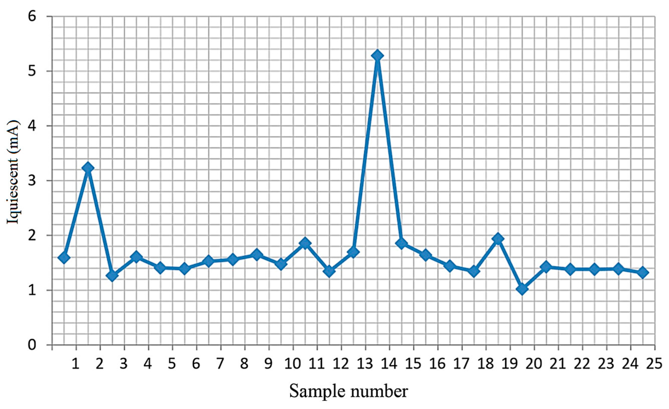
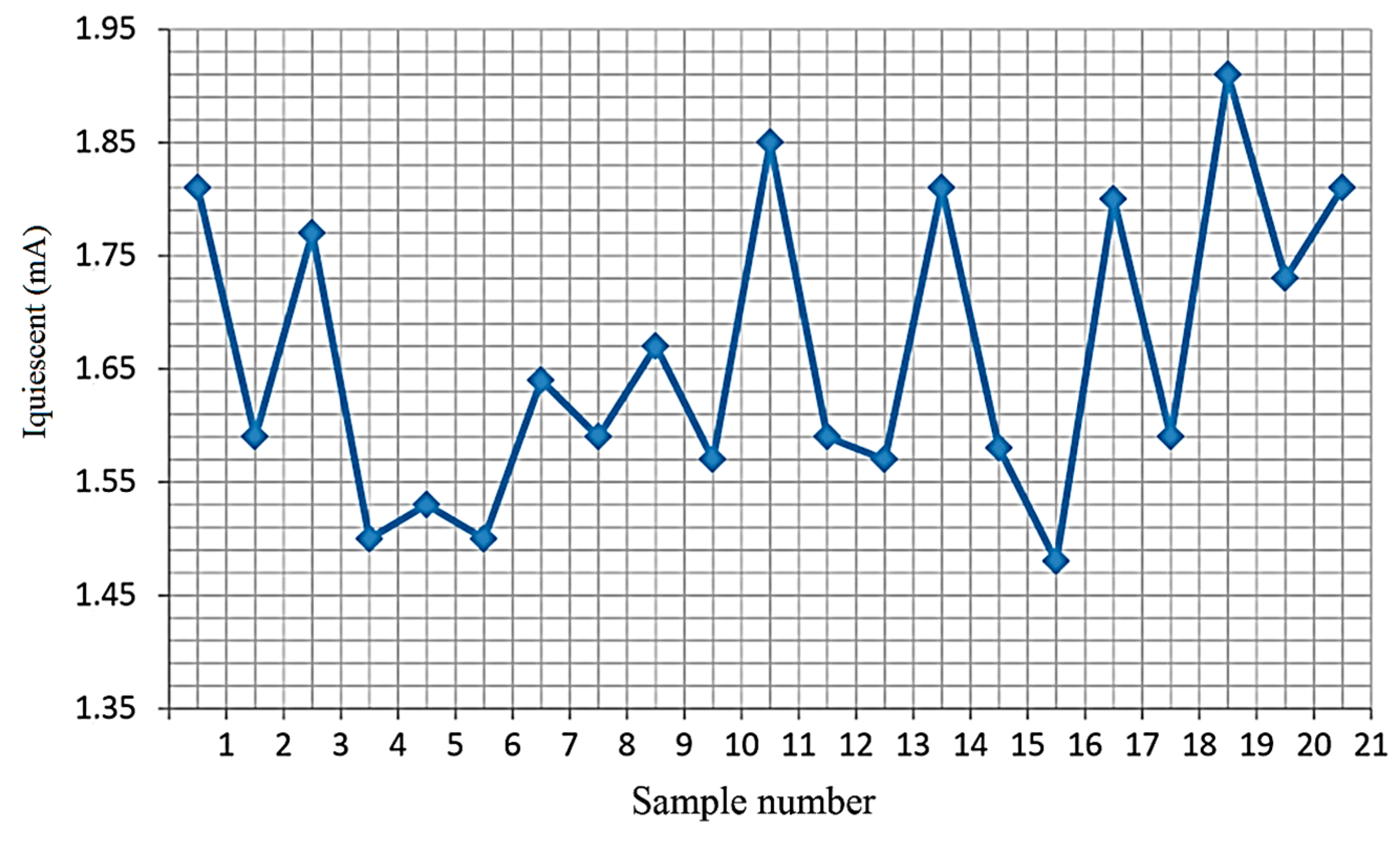
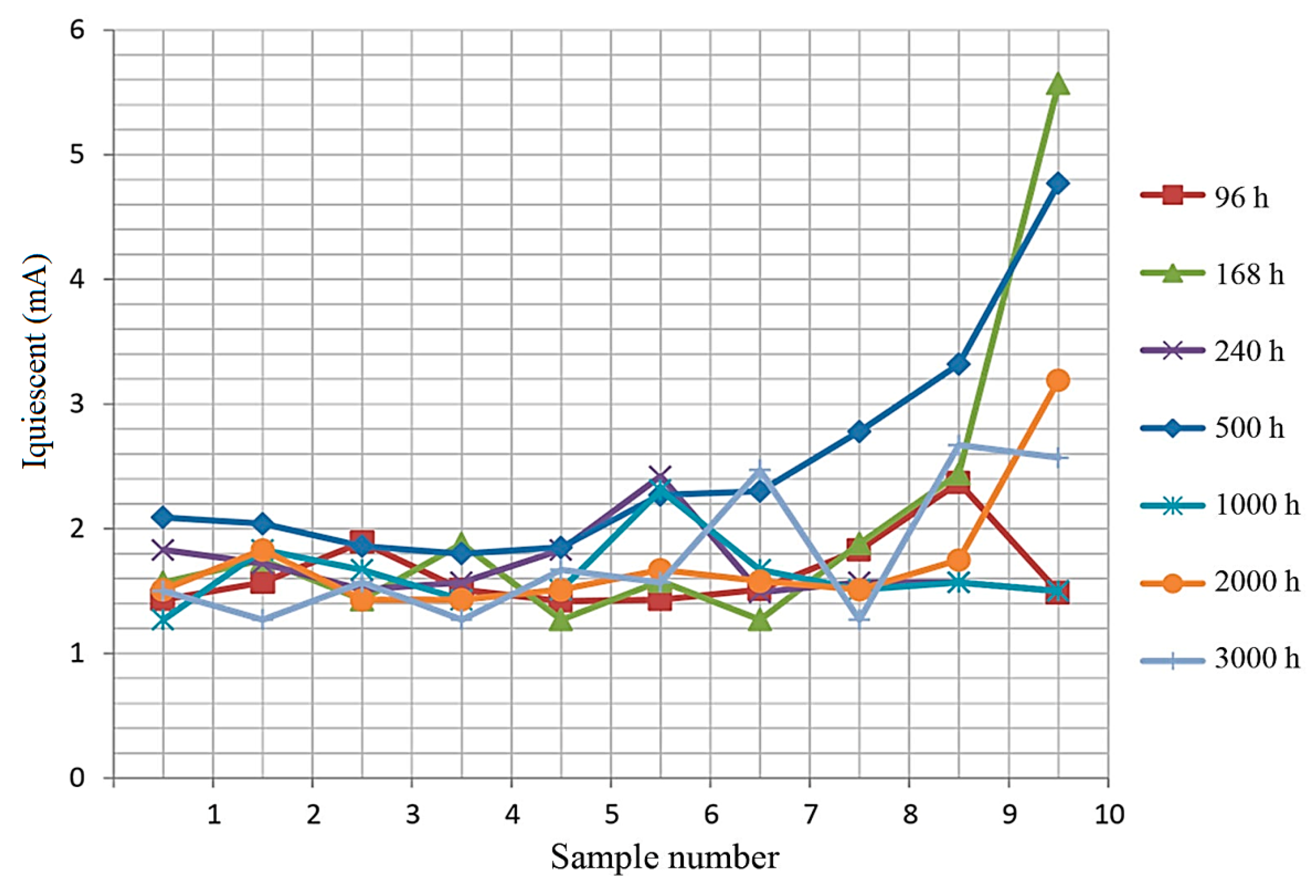
| Tout, h | ||||||
|---|---|---|---|---|---|---|
| 96 | 168 | 240 | 500 | 1000 | 2000 | 3000 |
| Iquiescent, mA | ||||||
| 1.43 | 1.57 | 1.83 | 2.09 | 1.27 | 1.51 | 1.5 |
| 1.57 | 1.75 | 1.72 | 2.04 | 1.83 | 1.83 | 1.27 |
| 1.89 | 1.43 | 1.51 | 1.86 | 1.67 | 1.43 | 1.57 |
| 1.51 | 1.88 | 1.57 | 1.8 | 1.43 | 1.43 | 1.27 |
| 1.42 | 1.27 | 1.83 | 1.85 | 1.51 | 1.51 | 1.67 |
| 1.43 | 1.58 | 2.42 | 2.27 | 2.31 | 1.67 | 1.57 |
| 1.51 | 1.27 | 1.49 | 2.3 | 1.67 | 1.58 | 2.47 |
| 1.83 | 1.88 | 1.57 | 2.78 | 1.51 | 1.51 | 1.27 |
| 2.37 | 2.44 | 1.57 | 3.32 | 1.57 | 1.75 | 2.67 |
| 1.49 | 5.57 | 1.5 | 4.77 | 1.5 | 3.19 | 2.57 |
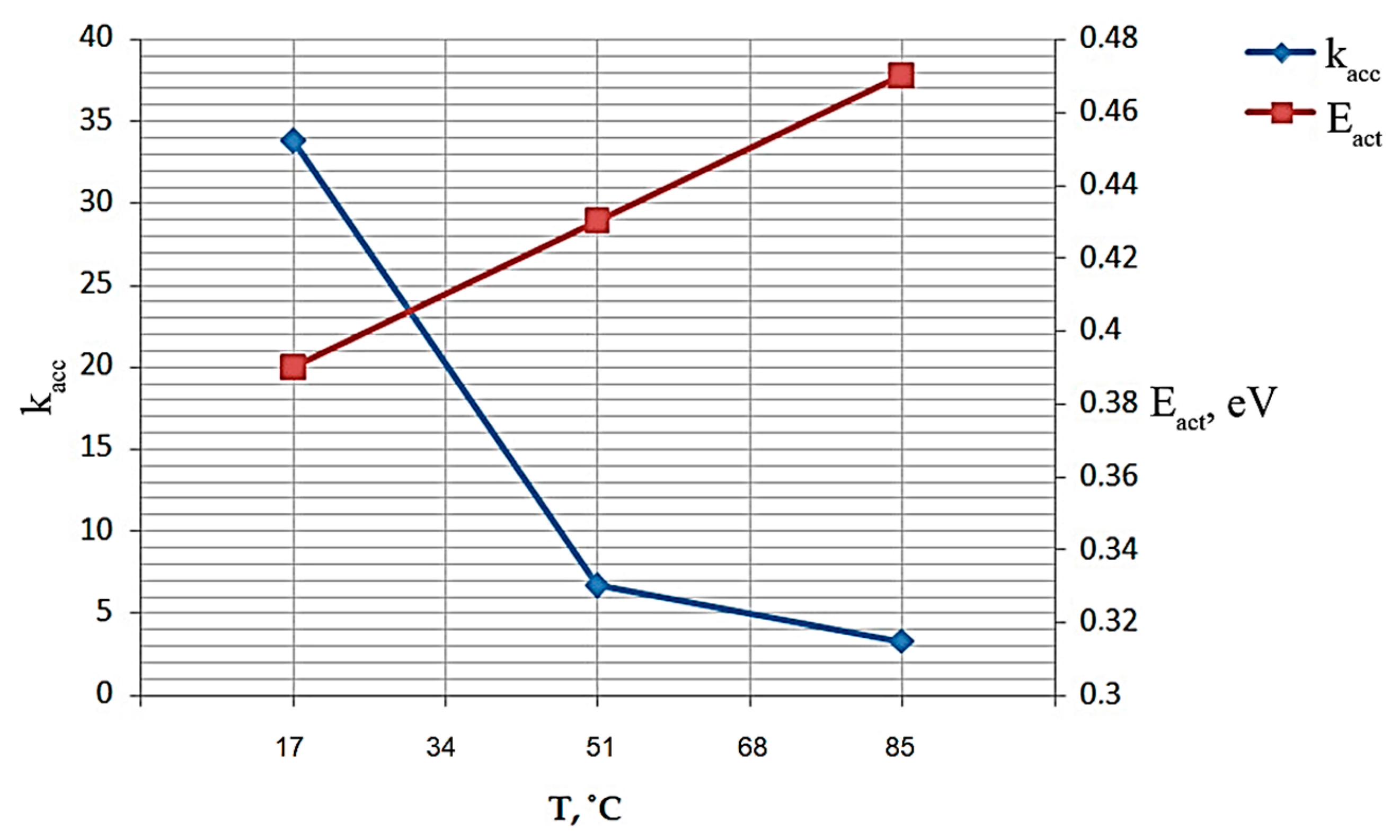
| T, °C | |||||
|---|---|---|---|---|---|
| 25 | 65 | 85 | 115 | 125 | |
| Ea, eV | 0.39 | 0.43 | 0.47 | 0.5 | 0.52 |
| T, °C | |||
|---|---|---|---|
| 25 | 65 | 85 | |
| kacc | 33.8 | 6.7 | 3.25 |
Disclaimer/Publisher’s Note: The statements, opinions and data contained in all publications are solely those of the individual author(s) and contributor(s) and not of MDPI and/or the editor(s). MDPI and/or the editor(s) disclaim responsibility for any injury to people or property resulting from any ideas, methods, instructions or products referred to in the content. |
© 2024 by the authors. Licensee MDPI, Basel, Switzerland. This article is an open access article distributed under the terms and conditions of the Creative Commons Attribution (CC BY) license (https://creativecommons.org/licenses/by/4.0/).
Share and Cite
Malozyomov, B.V.; Martyushev, N.V.; Bryukhanova, N.N.; Kondratiev, V.V.; Kononenko, R.V.; Pavlov, P.P.; Romanova, V.V.; Karlina, Y.I. Reliability Study of Metal-Oxide Semiconductors in Integrated Circuits. Micromachines 2024, 15, 561. https://doi.org/10.3390/mi15050561
Malozyomov BV, Martyushev NV, Bryukhanova NN, Kondratiev VV, Kononenko RV, Pavlov PP, Romanova VV, Karlina YI. Reliability Study of Metal-Oxide Semiconductors in Integrated Circuits. Micromachines. 2024; 15(5):561. https://doi.org/10.3390/mi15050561
Chicago/Turabian StyleMalozyomov, Boris V., Nikita V. Martyushev, Natalia Nikolaevna Bryukhanova, Viktor V. Kondratiev, Roman V. Kononenko, Pavel P. Pavlov, Victoria V. Romanova, and Yuliya I. Karlina. 2024. "Reliability Study of Metal-Oxide Semiconductors in Integrated Circuits" Micromachines 15, no. 5: 561. https://doi.org/10.3390/mi15050561