1. Introduction
Micro/nanofabrication technologies are indispensable for fabricating functional electronic, optical, medical and biochemical devices. Among these, high-aspect-ratio fabrication methods have been developed. These methods include deep-reactive ion etching (DRIE) [
1,
2], X-ray lithography [
3,
4,
5], UV lithography [
6,
7,
8,
9] and laser abrasion [
10,
11]. Because these fabrication methods provide low-throughput and are not cost-effective, successive molding technologies, such as injection molding, hot embossing and UV imprinting [
3,
7,
8,
9,
12,
13,
14,
15,
16,
17,
18,
19,
20,
21,
22,
23] are required for mass production. However, molding high-aspect-ratio structures is challenging, because it is difficult to successfully demold the structure.
The fabricated master is often replicated in another material, and the replicated sample is used as a mold. Nickel is commonly used as a mold material, with such molds formed using electroplating. Generally, because the master is entirely etched after the electroplating process, only one nickel mold can be obtained from a master. On the other hand, polymer replica molds are more cost-effective, because it is expected that polymer materials can be used to replicate a master or a nickel mold many times. The polymer materials include polydimethylsiloxane (PDMS) [
9,
16,
17], photocurable polymers [
15,
16,
20,
22] and thermoplastics [
18,
19,
21]. The molds require good mold releasability during demolding. In addition, a flexible polymer mold is expected to be applied to a roll-to-roll or roll-to-sheet process, which is suitable for mass production [
19,
22,
23].
In this study, UV imprinting methods for the fabrication of a high-aspect-ratio pillar array were demonstrated. The aspect ratios of the pillar and space were about four and ten, respectively. PDMS was selected for the mold, because of its good mold releasability and high flexibility. The following sections explain our experimental methodology, present and discuss our results and provide a conclusion.
2. Experimental Section
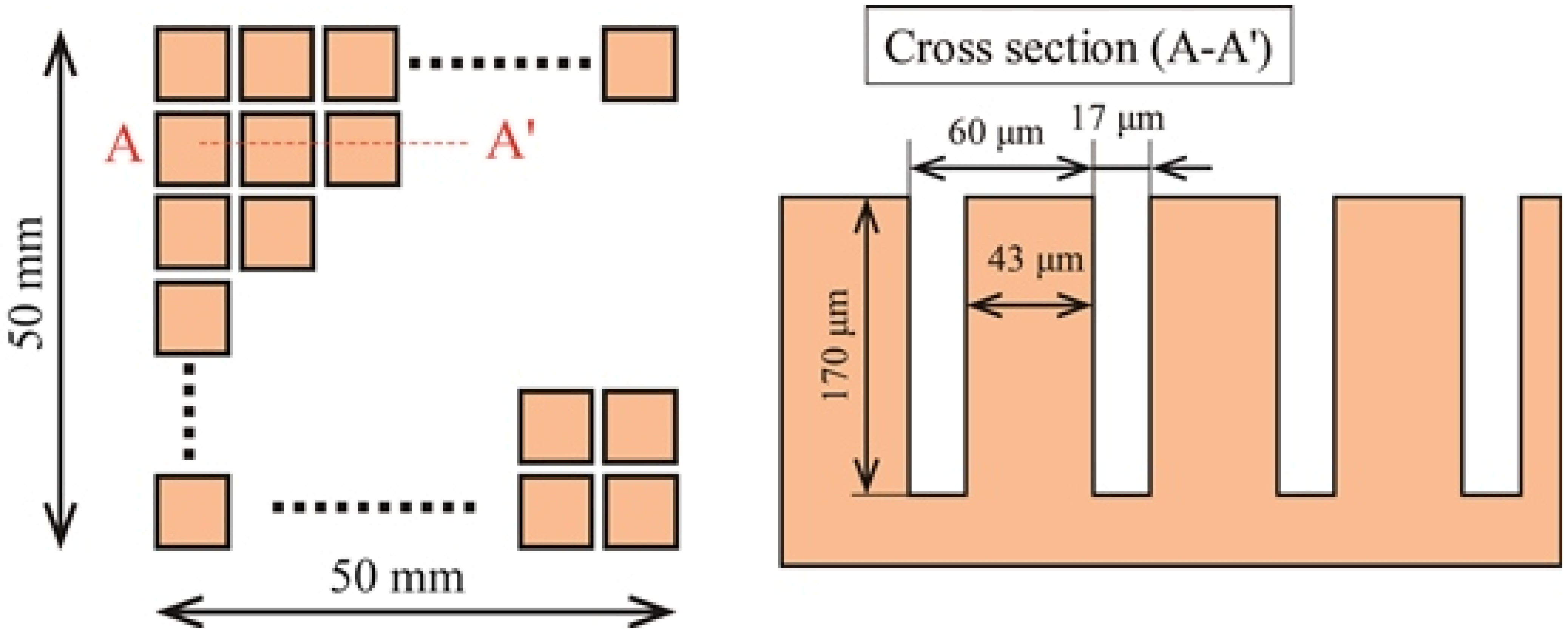
Figure 1 shows the design of a sample containing a high-aspect-ratio pillar array. The pattern area is 50 × 50 mm
2. The dimensions of the square prism-type pillars are 43 × 43 × 170 µm
3 and the pillars form a grid-like array with a 60 µm pitch.
Figure 1.
Design of sample having high-aspect-ratio pillar array.
Figure 1.
Design of sample having high-aspect-ratio pillar array.
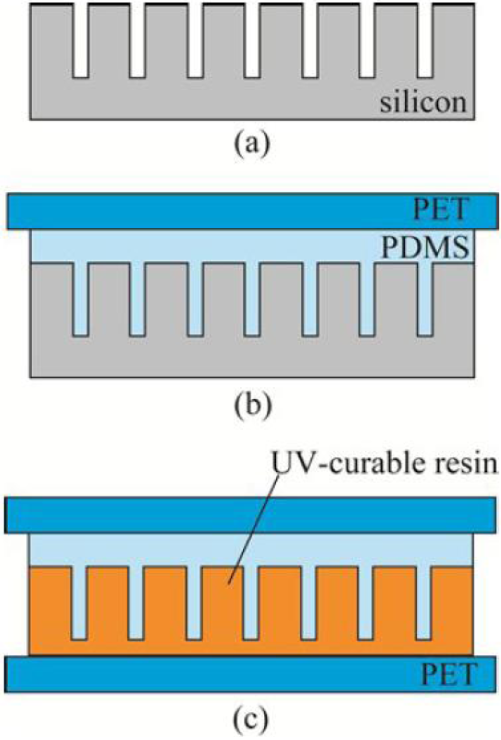
Figure 2 shows the fabrication process for the sample. The master pillar structure was fabricated on a silicon wafer (
Figure 2a). A positive-type photoresist was patterned using a maskless lithographic system (STG-4(DL), Toshiba Machine Co., Ltd., Numadu, Japan). The silicon was etched by DRIE (MUE-21, Sumitomo Precision Products, Co., Ltd., Amagasaki, Japan). Next, the master was treated with an anti-sticking agent (Optool HD-1101Z, Daikin Industries, Ltd., Osaka, Japan). Then, a PDMS mold was cast from the silicon master (
Figure 2b). The PDMS base (SIM260, Shin-Etsu Chemical Co., Ltd., Tokyo, Japan) and curing agent (CAT260, Shin-Etsu Chemical Co., Ltd., Tokyo, Japan) were mixed at a weight ratio of 10:1. After degassing in a vacuum chamber, the mixture was poured onto the master and degassed again. Then, a 100-µm-thick polyethylene terephthalate (PET) film (A4100, Toyobo Co., Ltd., Osaka, Japan) was applied to the uncured PDMS as a base film for the mold. The PET film had been treated with a primer (X-33-197, Shin-Etsu Chemical Co., Ltd., Tokyo, Japan) in advance. After curing at 80 °C for 1 h, the PDMS and PET were peeled off the master and baked again at 80 °C for 1 h. The thickness of the PDMS film was about 500 µm. Finally, a pillar array was UV-imprinted on the PET film using the PDMS mold (
Figure 2c). The central wavelength of the UV used to cure the resin was 365 nm.
Figure 2.
Outline of fabrication process: (a) silicon master fabrication by deep-reactive ion etching (DRIE); (b) polydimethylsiloxane (PDMS) mold fabrication by casting; (c) sample fabrication by UV imprinting.
Figure 2.
Outline of fabrication process: (a) silicon master fabrication by deep-reactive ion etching (DRIE); (b) polydimethylsiloxane (PDMS) mold fabrication by casting; (c) sample fabrication by UV imprinting.
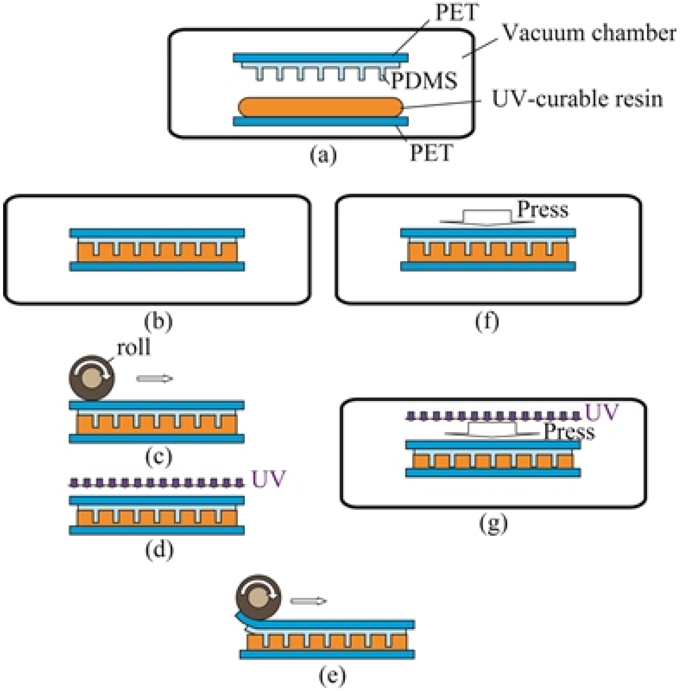
Figure 3 shows the details of the UV imprinting processes. First, 1 mL of epoxy-type UV-curable resin was dropped onto a PET film. The dropped area was 50 × 50 mm
2. The viscosity of this UV-curable resin was about 400 cps. The resin-coated PET film and the PDMS mold were set in a vacuum chamber (
Figure 3a). The PET was placed manually on the center of a stage in the chamber to lay the pattern area of PDMS mold on the resin-coated area during the next process. The PDMS mold was fixed to a motor that could have its vertical movement controlled from outside the chamber. After evacuating the chamber to a chamber pressure of about 200 Pa, the mold was placed into contact with the UV-curable resin (
Figure 3b). Then, the mold with the resin and PET substrate was taken out of the chamber and was pressed by rotating a roll from above (
Figure 3c). The force applied to the mold by rotating the roll was about 14 N, which corresponds to the weight of the roll. Then, the resin was cured by UV light irradiation without any load (
Figure 3d). Finally, the mold was peeled off manually along a roll with a diameter of 60 mm (
Figure 3e). The above-mentioned process is called the roll press method. To evaluate the applied force effects, the batch press method, which is described below, was also examined. The resin-coated PET film and PDMS mold were set in UV imprinting equipment (ST50, Toshiba Machine Co., Ltd., Numadu, Japan) (
Figure 3a). After evacuating the chamber, the mold was pressed at a set force,
F1 (
Figure 3f). The force was monitored by a load cell whose detection limit was 0.01 kN. After this, the resin was cured by irradiating UV light into the chamber while pressing the mold at force
F2 (
Figure 3g). Finally, the mold was peeled off along the roll (
Figure 3e).
Figure 3.
UV imprinting process: (a) placing PDMS mold and UV-curable resin-coated polyethylene terephthalate (PET) in a vacuum chamber; (b) moving mold and resin into contact under reduced pressure; (c) pressing by rotating roll; (d) UV irradiation; (e) peeling off mold along roll; (f) pressing mold and resin under reduced pressure; (g) UV irradiation and pressing. The roll press method includes (a), (b), (c), (d) and (e), and the batch press method includes (a), (f), (g) and (e).
To evaluate the evacuation effect during the filling process (
Figure 3b), a sample without evacuation was also prepared using the roll press method.
The heights, gaps and pitches of the pillars in the silicon master and imprinted sample were measured using a laser microscope (LEXT OLS3000, Olympus Co., Tokyo, Japan). As shown in
Figure 4a, five points in the pattern area were measured: point #1 was at the center, while points #2–4 were about 5 mm inside the edge of the pattern area. A vertical scan was carried out with a 0.5-μm resolution for measuring the height. At each measurement point, two base points, the center of the straight groove (α) and the center of the cross-junction of the groove (β) were selected (
Figure 4b).
The residual layer thickness (RLT) of the imprinted sample was measured from the scanning ion microscopic (SIM) image. This SIM image was obtained by using a focused ion beam system (FB-2100, Hitachi High-Technologies Co., Tokyo, Japan). The center of the pattern area was selected to measure the RLT. In the case of a sample fabricated by the roll press method, the uniformity of the RLT within a sample was also measured. The location from the edge of the pattern area (
x) was defined as shown in
Figure 4c, and 20 points (
x = 6–46) were measured.
Figure 4.
(a) Five measurement points for the silicon master and imprinted sample; (b) two base points for measuring pillar height; (c) definition of location from edge of pattern area (x) on the imprinted sample.
Figure 4.
(a) Five measurement points for the silicon master and imprinted sample; (b) two base points for measuring pillar height; (c) definition of location from edge of pattern area (x) on the imprinted sample.
3. Results and Discussion
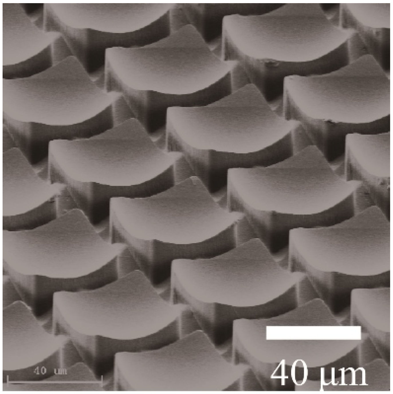
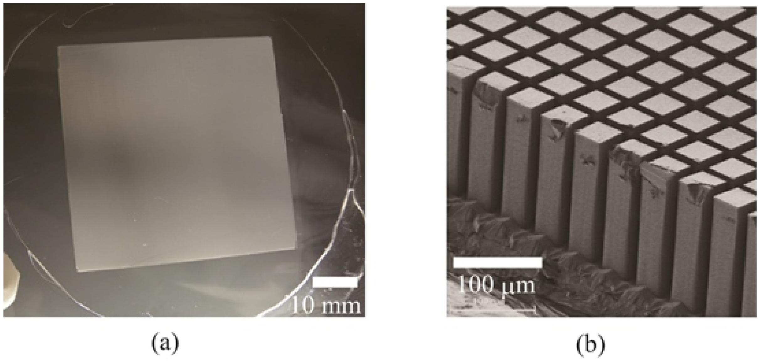
Figure 5 shows a photograph and SIM image of a sample imprinted by the roll press method. The pillar pattern was formed on the entire PET film area.
Table 1 lists the pattern sizes on the silicon master and the UV imprinted sample. The height based at point α (
hα) was different from that at point β (
hβ), because of a microloading effect during DRIE [
2,
24]. The heights for the imprinted samples were 1–2 µm higher than those for the silicon master, while the gaps and pitches showed little difference. This suggests that a PDMS or UV-curable resin pattern elongates during the demolding (from the silicon master in the case of PDMS and from the PDMS master in the case of UV-curable resin).
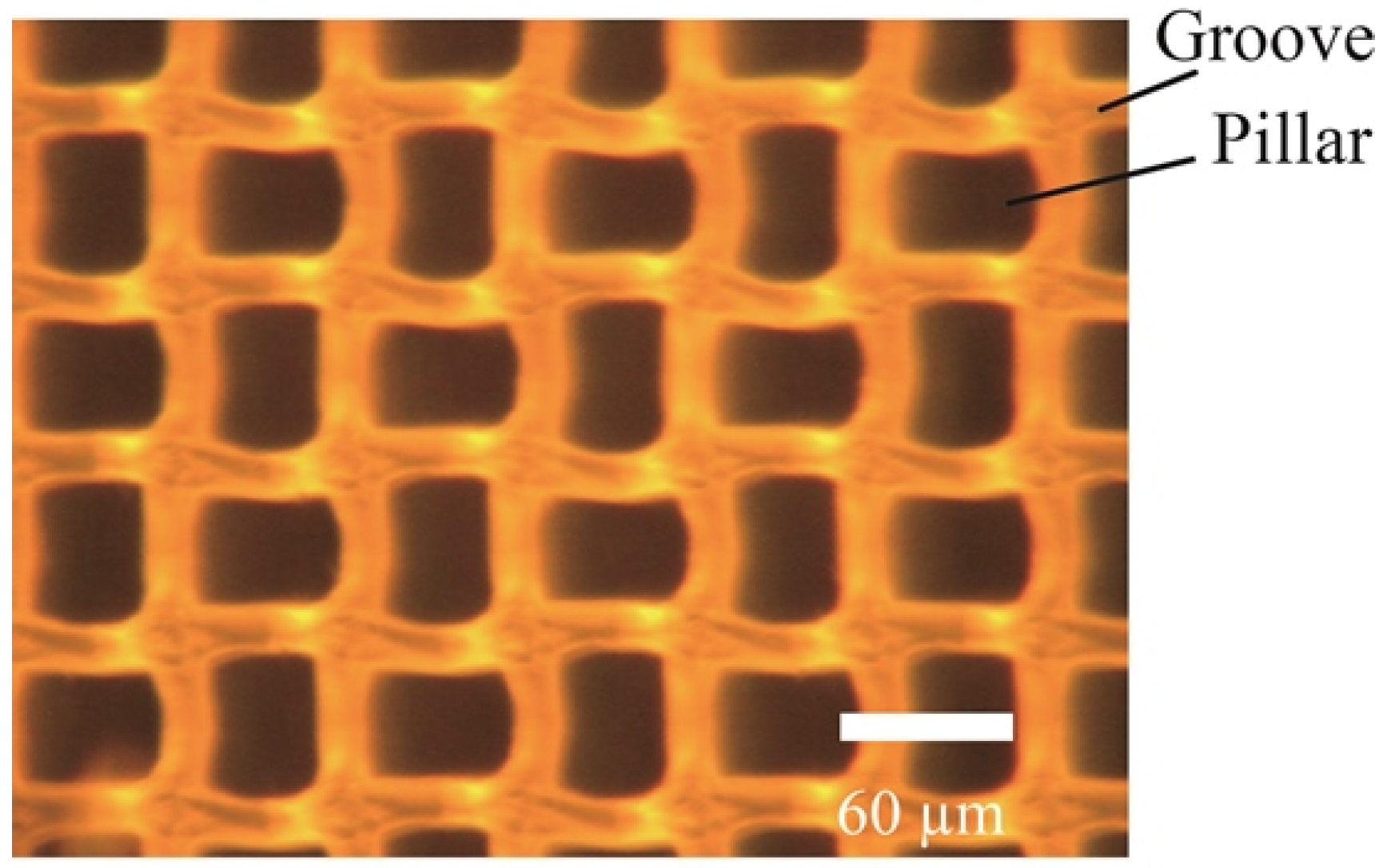
Figure 6 shows SIM images of samples molded without evacuation in
Figure 3b. The height of the pillar was only about 20 µm. This result indicates that filling the mold with resin under a reduced pressure was easier than under atmospheric pressure. The meniscus geometry in
Figure 6 suggests that a higher applied force was required to fill the mold with resin, which caused deformation of the PDMS mold structure.
On the other hand, the generation of bubbles in the uncured resin was grossly observed during the pressing of the mold and resin under the reduced pressure (
Figure 3b). After opening a leak valve in the chamber to expose it to atmospheric pressure, the generated bubbles decreased. These phenomena seem to have originated with the outgassing and gas absorption characteristics of PDMS. Thus, when the UV-curing was successively carried out under the reduced pressure (
Figure 3g), an unfilled pattern region like that shown in
Figure 6 was also often observed. A filled pattern like that shown in
Figure 5 was obtained over the pattern area when UV was irradiated after exposure to atmospheric pressure (
Figure 3d,g).
Figure 5.
(a) Photograph and (b) Bird’s-eye SIM image of the UV-imprinted sample.
Figure 5.
(a) Photograph and (b) Bird’s-eye SIM image of the UV-imprinted sample.
Table 1.
Sizes of patterns on the silicon master and UV imprinted sample.
Table 1.
Sizes of patterns on the silicon master and UV imprinted sample.
| Point No. | Height (µm) | Gap (µm) | Pitch (µm) |
|---|
| hα | hβ |
|---|
| Silicon master | | | | |
| 1 | 159.5 | 167.5 | 16.9 | 59.9 |
| 2 | 164.5 | 170.5 | 16.9 | 59.9 |
| 3 | 162.5 | 170.5 | 16.9 | 59.9 |
| 4 | 166.0 | 172.0 | 16.7 | 59.7 |
| 5 | 163.5 | 171.0 | 16.9 | 59.7 |
| Average | 163.2 | 170.3 | 16.9 | 59.9 |
| Imprinted sample | | | | |
| 1 | 161.0 | 170.0 | 16.9 | 59.9 |
| 2 | 164.5 | 170.5 | 16.9 | 59.9 |
| 3 | 164.0 | 172.5 | 16.9 | 59.9 |
| 4 | 166.5 | 173.5 | 16.7 | 59.7 |
| 5 | 165.5 | 174.0 | 16.9 | 59.7 |
| Average | 164.3 | 172.1 | 16.9 | 59.9 |
Figure 6.
Bird’s-eye SIM images of the sample molded without evacuation.
Figure 6.
Bird’s-eye SIM images of the sample molded without evacuation.
Figure 7.
Photomicrograph of the sample imprinted at F1 = F2 = 0.50 kN.
Figure 7.
Photomicrograph of the sample imprinted at F1 = F2 = 0.50 kN.
Figure 7 shows a photomicrograph of a sample imprinted at
F1 =
F2 = 0.50 kN. Deformation of the pillar structure was observed. This deformation originated with the deformation of the PDMS pattern during pressing. Thus, it disappeared when no force was applied during UV-curing (
F2 = 0.00 kN). The following samples were all examined at
F2 = 0.00 kN.
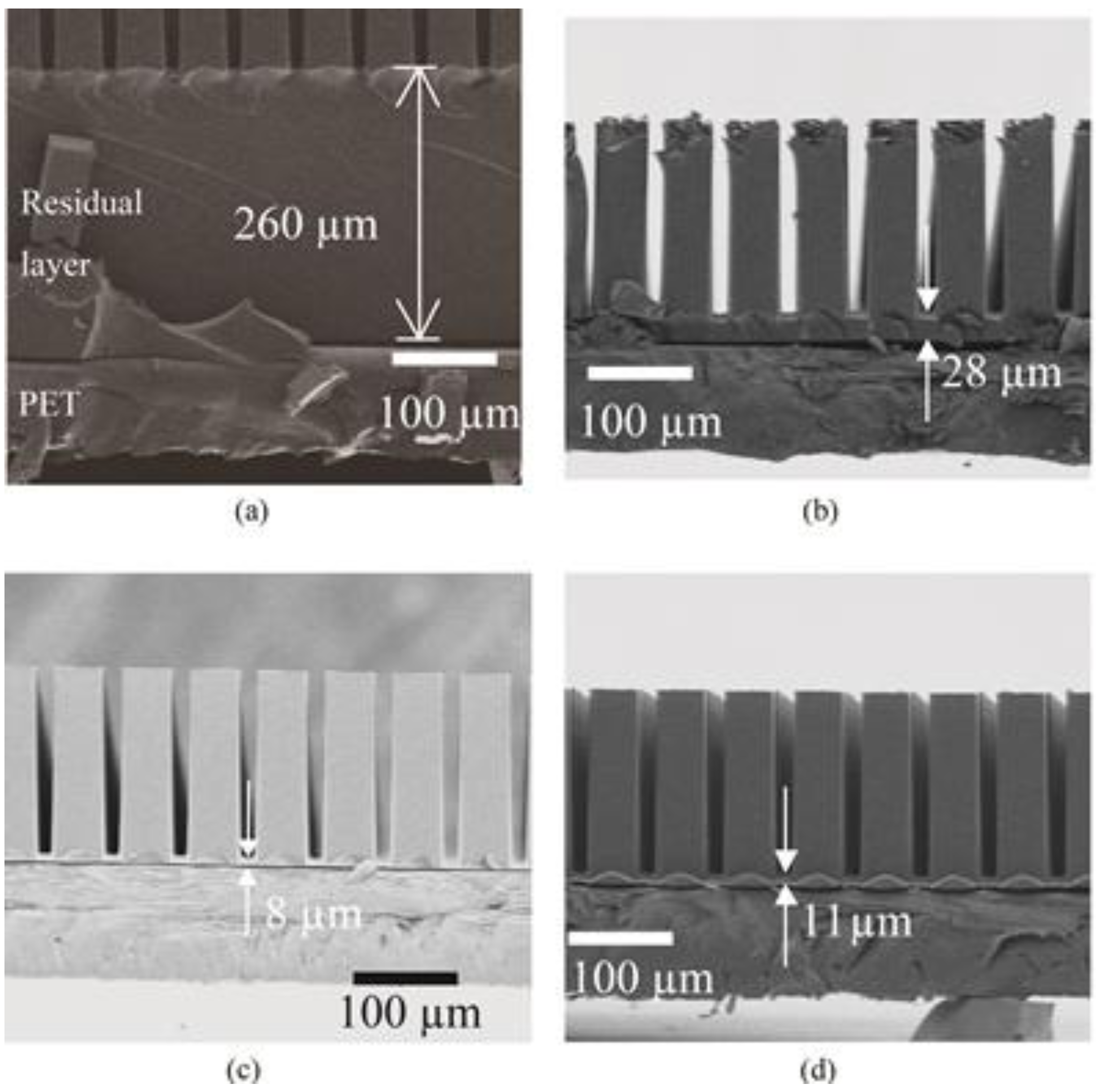
Figure 8 shows cross-sectional SIM images of samples imprinted at various applied forces (
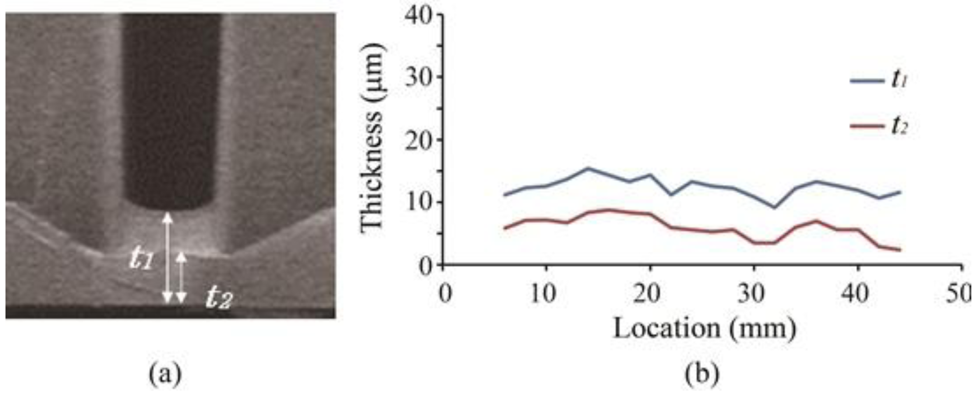
F1). Two types of RLTs were defined, as shown in
Figure 9a. The thicker (
t1) and thinner (
t2) RLTs correspond to the points at α and near β in
Figure 4b, respectively. Each
t1 is shown in
Figure 8. The RLT decreased with an increase in
F1 (
Figure 8a–c). The applied pressures were 4 kPa at
F1 = 0.01 kN and 180 kPa at
F1 = 0.45 kN, given the fact that the pressed area was 50 × 50 mm
2. The thickness of the roll pressed sample (
Figure 8d) was close to that of the batch pressed sample at
F1 = 0.45 kN, while the pressure was 3.2-times smaller (56 kPa), given the fact that the pressed area between the mold and roll was 5 × 50 mm
2.
Figure 9b shows the measured
t1 and
t2 within a sample. The average values of
t1 and
t2 were 12.4 ± 1.5 µm and 5.8 ± 2.0 µm, respectively. Note that these values may include a variation of the thickness of the as-coated resin. The value of
t2 also included a variation based on the sectional location, with a thicker
t2 found for a sectional location closer to the pillar. However, at least the residual layer corresponding to the difference between
t1 and
t2 (=6.5 µm) will remain, even if a higher force is applied in the roll press method. To further decrease RLT, the bottom geometry should be flatter. From this point of view, other master fabrication methods, such as X-ray lithography [
3,
4,
5] and UV lithography [
6,
7,
8,
9], would be more appropriate than the DRIE method.
These results indicate that both the batch and roll press methods are available for fabricating this pillar array. For application to larger pattern areas, it is expected that the roll press process would be more appropriate than the batch process in terms of pressure uniformity [
25,
26]. In the roll press method, several independent product lines corresponding to
Figure 3 will be required for mass production.
Figure 8.
Cross-sectional SIM images of samples: (a) without pressing (with mold and resin simply in contact); with batch pressing at (b) F1 = 0.01 kN and (c) F1 = 0.45 kN; and (d) with roll pressing.
Figure 8.
Cross-sectional SIM images of samples: (a) without pressing (with mold and resin simply in contact); with batch pressing at (b) F1 = 0.01 kN and (c) F1 = 0.45 kN; and (d) with roll pressing.
Figure 9.
(a) Definitions of two types of residual layer thicknesses (RLTs) and (b) RLTs within the roll-pressed sample.
Figure 9.
(a) Definitions of two types of residual layer thicknesses (RLTs) and (b) RLTs within the roll-pressed sample.
Because the cost of a PDMS mold, it could be used for UV imprinting over 10 times without remarkable pattern deformation. When used more than 10 times, the PDMS was often partially peeled away from the PET during demolding. The PDMS film at the border between the unpeeled and peeled portions was subject to irreversible stretching or tearing during the next demolding process. Thus, an improvement in the adhesion strength between the PDMS and the PET will be required for further multiple uses, which is important for cost reduction. Examples of alternatives include the sol-gel method [
27] and a method that does not use a base film. In the latter case, the PDMS film would need to be thicker from the viewpoint of morphological stability and handling ability.


