1. Introduction
An alternative approach to standard microfabrication techniques, such as wet and dry etching, is represented by soft lithography. Soft lithography, pioneered by Whitesides and co-workers [
1], is a group of fabrication methods for forming structures with feature sizes generally at micro-metric scale. The idea underlying the fabrication method is to realize a negative of the design to be transferred, called master, and then use it to imprint the pattern directly by bringing in contact the hard master and a soft surface. Currently, soft lithography is one of the most used techniques for realizing microfluidic devices and sophisticated chips, using a simple replica molding process from an hard master [
2,
3]. Polydimethylsiloxane (PDMS) is key material in the replica molding technique [
4], due to its properties: PDMS is transparent, easy to handle, and most of all is very cheap as material. High costs are the major drawback of photolithography technology since related instrumentation and processes are very expensive: in a device development cycle, main costs and times are due to photomasks realization and photolithographic equipment.
Many maskless photolithography approaches, typically based on UV laser direct writing coupled by motorized stages [
5,
6,
7,
8], have been proposed, but since the mask approach results the most simple and practical method, innovative ideas have been suggested. Qin
et al. [
9] described how image setting system can be useful to generate mask with feature sizes larger than 20 µm. This limit has been reduced using high resolution photoplotter printers as demonstrated by Linder
et al. [
10]. Fan
et al. [
11] illustrated a new technique for masking deep-UV exposure of poly(methylmethacrylate) (PMMA) using a printed wax mask. One of the most interesting works describing a new method for fabrication of cheap contact photomasks using photographic films was published by Deng
et al. [
12]. Computer aided designed (CAD) files were first printed bigger than real size onto paper using an office printer with resolution of 600 dots/in, and then reduced by a 35mm camera to the required dimensions onto 35 mm films. After development, these photographic films were used as photomasks in contact photolithography. Even if the resolution claimed by authors is of 15 µm and therefore distant from the few microns resolution needed to fabricate complex microfluidic devices, the procedure is well suited for many medium resolution applications, such those typical required in microfluidics. The photo reduction method has used since 1960s for Rubylith films when printers did not have a sufficient resolution to create complex patterns. Pattern generation was a tedious manual process. Moreover the large Rubylith master needed to be reduced many times using a large reduction copy camera [
13]. Following Deng’s work, many others [
14,
15,
16] tried to improve performances.
This method could be compared with photoplotter, mask writer and electron beam lithography. Several parameters influence the cost-performance ratio, e.g., the feature minimum resolution, time elapsed for a mask production, the costs fixed and variable, and operation complexity. Of course this technique has the resolution of about 20 μm, less than obtainable by the above-mentioned equipment which is in the order of 10 μm, 1 μm and 10 nm respectively. Moreover, it is also two-three orders of magnitude less expensive than the costs sustained by other equipment considered above. The resolution of this method is sufficient for typical microfluidics applications, which is in the order of tens of microns. Concerning other above-mentioned aspects the mask production with this method has a very low complexity, requires a minimum training period and typically the process takes few minutes.
In this paper, we improve this low-cost mask fabrication introducing fine control in the reduction factor from paper to photographic film based on the use of a photographic enlarger (Durst C35) used in reverse mode in darkroom. High contrast silver-halide based photographic films are exposed and processed in order to optimize the technique. The produced contact photomasks have been optically characterized. We also demonstrate the effective combination of photomask with UV light box for master development in microfluidic applications.
2. Materials and Methods
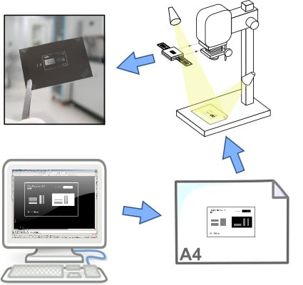
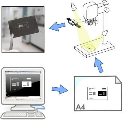
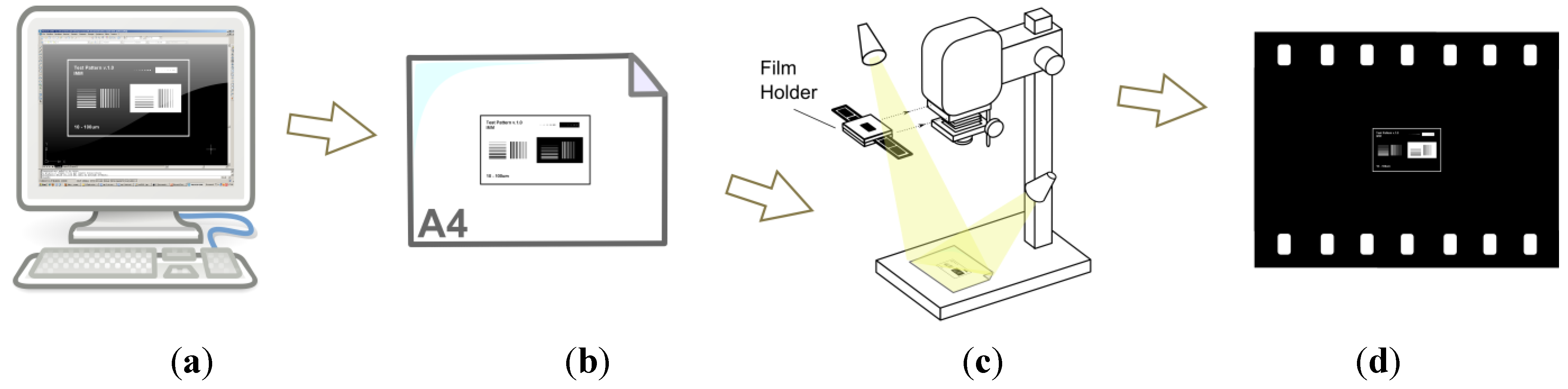
The development process of our photomasks is schematized in
Figure 1: a CAD file has been first printed bigger than real size onto paper using an office printer with resolution of 1200 dots/in, and then reduced to the required dimensions onto photographic films.
Figure 1.
(a) Computer aided designed (CAD) design of mask patterns; (b) Scaled print (typically 10:1) of the mask patterns on a paper sheet; (c) Mask patterns optical reduction and transfer from paper to film by reversal use of an enlarger; (d) The film photomask after the development process.
Figure 1.
(a) Computer aided designed (CAD) design of mask patterns; (b) Scaled print (typically 10:1) of the mask patterns on a paper sheet; (c) Mask patterns optical reduction and transfer from paper to film by reversal use of an enlarger; (d) The film photomask after the development process.
Photographic reduction has been performed by an enlarger, a specialized transparency projector was used to produce photographic prints from film or glass negatives using the gel-silver process. It consists of a light source, a film holder and a specialized objective (Rodenstock Rodagon
f = 50 mm). In our setup this instrument has been used in reverse mode, impressing a high contrast negative film (Maco Genius Print Film) housed in the film holder, by external light sources. The large patterned mask (8 × 13 cm), designed by CAD and laser printed on a high quality paper, is disposed on the enlarger image plane. We generally choose the smallest lens aperture (f/32
i.e., the focal length is 32 times the aperture diameter) as the diaphragm effect is to increase the Depth Of Focus (DOF) and this in turn obtains a less critical setup alignment [
17]. A suitable quantity of light is issued by the external illumination system composed of two 1250 lm incandescent lamps with parabolic mirrors which are oriented at 45° with respect to the image enlarger plane, providing a fairly uniform illumination of 1200 l× on the printed paper. Then, the light reflected from the white zones of paper is collected by the objective and focalized on the film holder impressing the negative film and creating a negative image of the mask with small feature size. The film holder used is a Mesixneg 35, a standard negative carrier consisting of a plastic frame with a rectangular 24 × 36 mm hole. Time exposure has been set to 40 s to obtain black enough zone to use it as a mask for UV light. The Maco film has been developed by Maco LP Superlith LPP70 for 3 min and then fixed for 2:30 min in Ilford Rapid Fixer to make the image permanent and light-resistant by dissolving any remaining silver halide salts.
The transmittance of these photomasks has been measured using a spectroscopic ellipsometer in transmission mode (UVISEL, Horiba-Jobin-Yvon), while their thicknesses have been measured by Kla-Tencor Profilometer. The fabricated photographic masks have been used in an UV light box avoiding the use of an expensive mask aligner. UV light boxes are normally used for printed circuit boards and are simply composed by UV lamps without any light collimation system. The designed system was replicated by photolithographic process on a 10 µm thick negative photoresist (SU-8 2007, MicroChem Corp.) spin-coated for 30 s at 1800 rpm on a silicon substrate. After the photoresist development, the silicon wafer was silanized on exposure to chlorotrimethylsilane (Sigma-Aldrich Co.) vapor for 10 min as anti-sticking treatment. A 10:1 mixture of PDMS prepolymer and curing agent (Sylgard 184, Dow Corning) was prepared and degassed under vacuum for 1h. The mixture was poured on the patterned wafer and cured on a hot plate at 80 °C for 2 h to facilitate the polymerization and the cross-linking process. After the PDMS layer peeling, inlet and outlet holes were drilled through it in order to allow the access of liquid substances to the system. The surfaces of PDMS layer were bonded on to a glass slide by exposing their surfaces to oxygen plasma for 10 s.
3. Results and Discussion
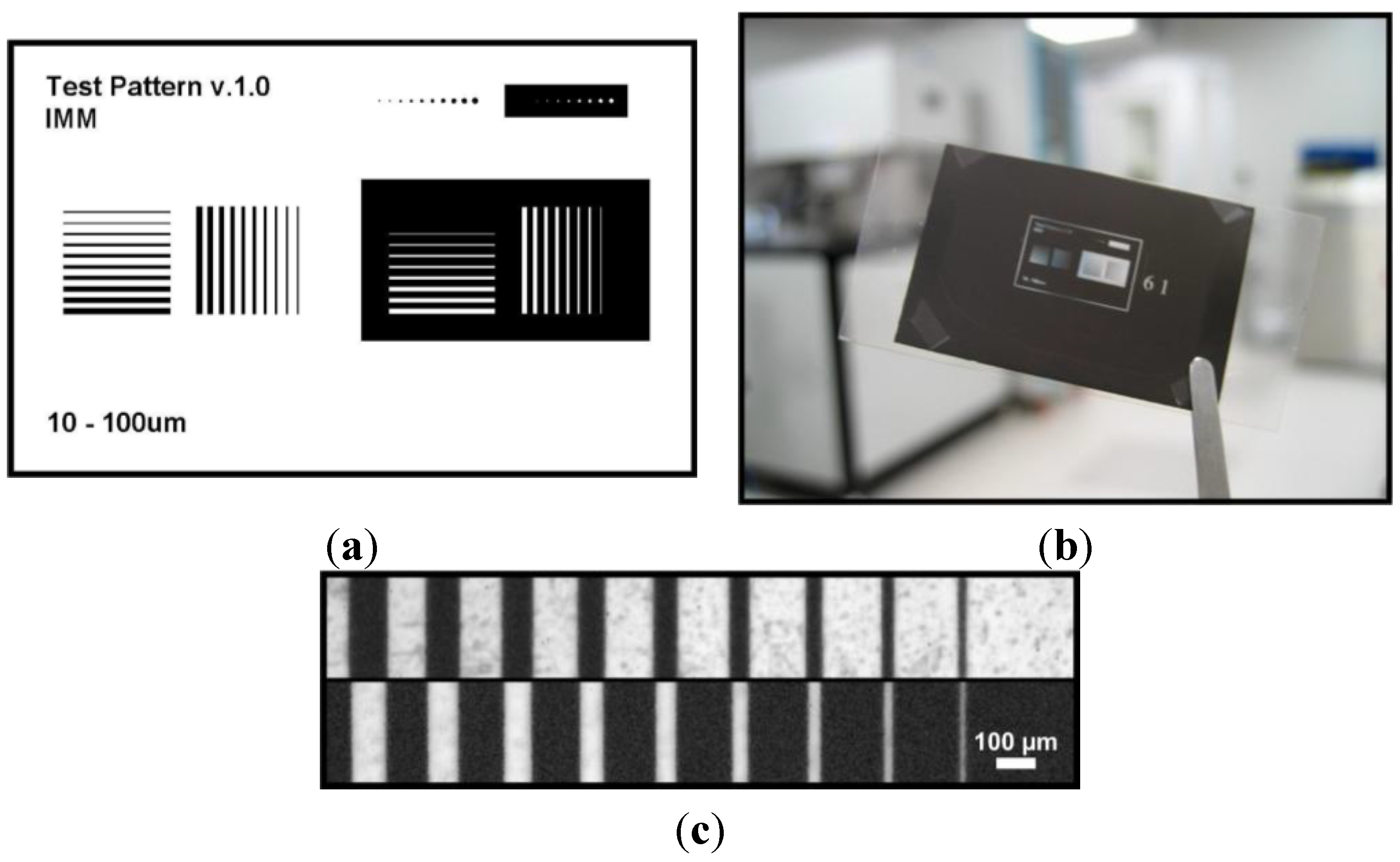
A reduction factor of 10 has been generally chosen for masks realization. Our setup allows a maximum factor of 13; greater reduction factors can been achieved using multiple reduction steps, underlining that the minimum pitch achievable, due to overall limits of this fabrication procedure, is still 20 µm. By comparing the dimensions of a developed film and its image projected by the objective, we have also estimated that our setup, made up basically by the photographic enlarger, produces a reduction error under 0.7%. This very low reduction error, which unfortunately we can not compare since it is never reported in other published papers using 35 mm conventional cameras, ensures a quite good control on the size of the microsystem fabricated. The resolution limit of the enlarger lens caused by diffraction has been calculated to be about 4 µm. However, the experimental limit is probably higher due to aberrations. A test pattern (
Figure 2a), inspired to “1951 USAF” resolution test chart, has been designed and transferred onto photographic film (
Figure 2b), using the described technique, in order to optimize the process parameters. The film is half tones without gray scale, and orthochromatic, which means that is sensitive to only blue and green light, and thus can be processed in darkroom with a red safelight. This kind of film allows us to achieve good quality masks [
16].
Figure 2.
(a) Test pattern used for optimize the reduction parameter. It contains lines and dots in black and white with dimensions from 10 µm to 100 µm. (b) Photo of the impressed photographic film. (c) Optical image of test pattern lines.
Figure 2.
(a) Test pattern used for optimize the reduction parameter. It contains lines and dots in black and white with dimensions from 10 µm to 100 µm. (b) Photo of the impressed photographic film. (c) Optical image of test pattern lines.
The test pattern contains four groups of ten lines and two groups of dots in black and white; line size ranges from 10 µm to 100 µm, where the Maco film resolution is 300 lp/mm.
Figure 2c shows the optical image of test pattern lines: the minimum pitch reproducible is of 20 µm. Photographic films are based on silver-halide crystals embedded in a gelatin layer, commonly known as the photographic emulsion. Actually, the photosensitive emulsion is not really an “emulsion” but rather a thin film of silver-halide microcrystals dispersed in a colloid (gelatine). The emulsion is coated on a flexible substrate material. Dark (exposed) regions of the film are due to small particles of metallic silver, developed from silver halide, that have received enough photons [
18].
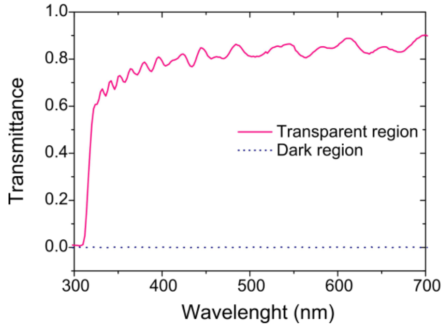
Figure 3 shows the transmittance by transparent and dark regions of photomask in the near UV and optical wavelength range. Starting from 325 nm, the transmittance in the transparent region is higher than 60%, while in the dark region is lower than 0.2% in the whole wavelength range examined.
Figure 3.
Transmittance of photomask in the transparent and dark regions.
Figure 3.
Transmittance of photomask in the transparent and dark regions.
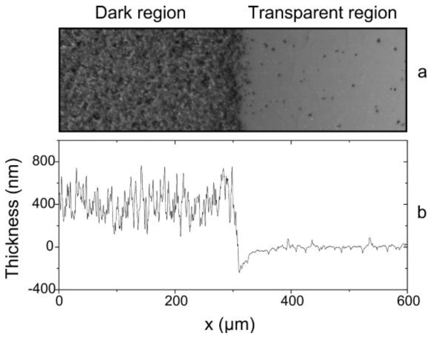
This confirms the suitability of photographic films to be used as masks in photolithographic processes. Small amplitude modulation of transmission spectrum shown is due to interference effects produced by the film thickness. In
Figure 4a it is possible to observe the optical image of the film which is clearly composed by grains that are obviously absent in classical photolithographic masks. It has an average thickness of 410 nm and a roughness of 120 nm (see
Figure 4b), measured by profilometer.
Figure 4.
(a) Optical photograph and (b) thickness profiles measured by the profilometer of the transition from dark exposed region to transparent unexposed region on the photographic film.
Figure 4.
(a) Optical photograph and (b) thickness profiles measured by the profilometer of the transition from dark exposed region to transparent unexposed region on the photographic film.
Using free images analysis software (ImageJ 1.46) on a high resolution (100×) optical microphotograph (not shown here), black dots with a diameter from 0.4 µm to 3.2 µm have been found and measured in the transparent region. These film defects, which would be transferred by the mask aligner on to the photoresist, can be disregarded by using the UV box: in this case the uncollimated light from the illumination system “erases” all micron and submicron features present on the mask. This is a disadvantage for high-resolution photolithography but it turns in an advantage for low-resolution applications. The measure of the length for the edge transition region (from dark to transparent) in photographic films is 10 µm and this limits the minimum feature achievable to 20 µm. The length of edge transition regions can also be affected by the presence of mechanical vibrations that seriously affect the image transfer at this scale.
The test pattern designed was replicated by photolithographic process on a 10 µm thick SU-8 photoresist on silicon substrate. This photoresist is often used to fabricate masters for microfluidic applications; it allows to reproduce micro- and nano-structure having a wide range of thicknesses (0.5 to 650 µm with a single coat process) [
19]. Exposure to UV light for 20 s has been realized in the UV light box. We never observed thermal deformation of photomasks, at least in the macroscopic range, after UV exposure. Tests have been performed to found the correct process parameters (exposure, bake and development times). Although in the photographic mask, the edge are not so well defined due to the presence of the transition region from dark to transparent zones (
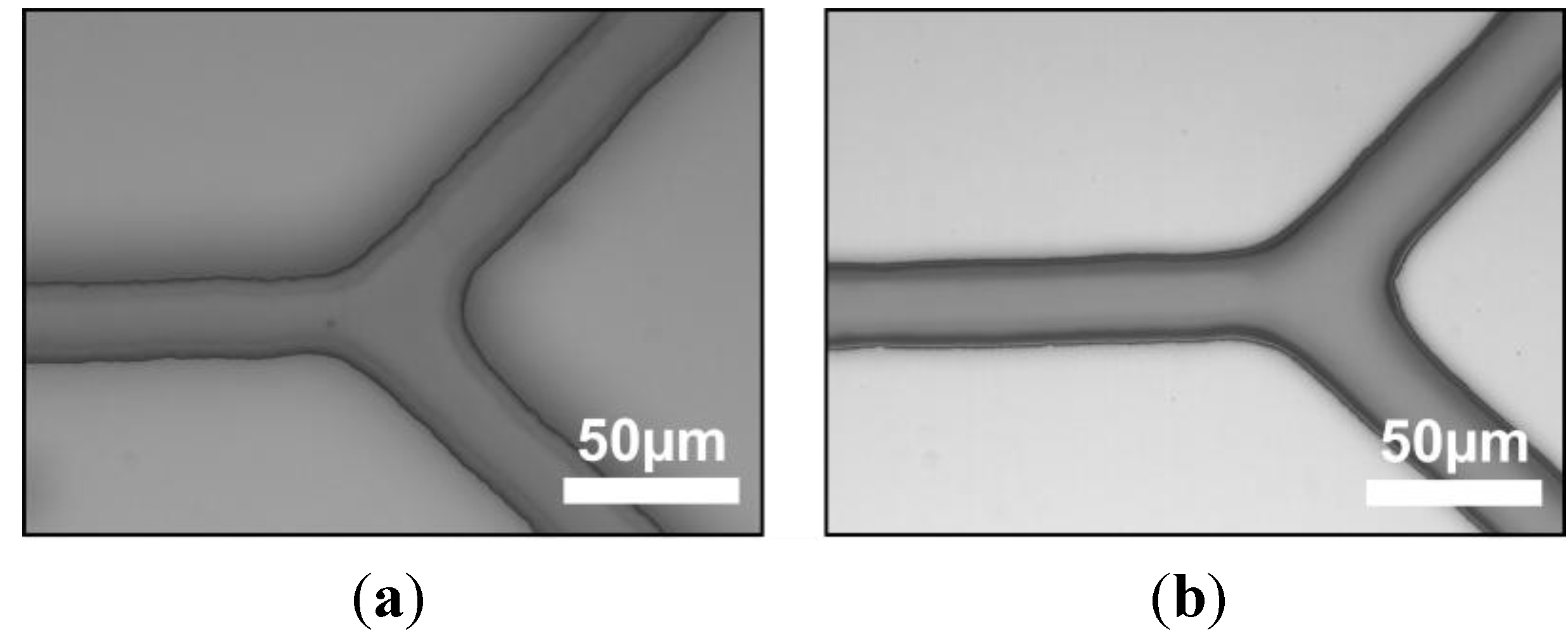
Figure 4a), the impressed photoresist edges appear quite well defined. To compare UV box with mask aligner capabilities, a photographic mask, containing a 20 µm y-shape structure, has been used on both instruments.
Figure 5 shows the optical image of the impressed photoresist by the mask aligner (Karl Suss MA6) and the UV box: the comparison shows that the edge roughness is strongly reduced when UV box is used (see
Figure 5b), instead, an irregular edge (due to mask imperfections) appears in the sample realized with a professional mask aligner (see
Figure 5a).
Figure 5.
SU-8 Y-shape channel impressed with the same mask using (a) the mask aligner and (b) the UV Box (SU-8, thickness: 10µm).
Figure 5.
SU-8 Y-shape channel impressed with the same mask using (a) the mask aligner and (b) the UV Box (SU-8, thickness: 10µm).
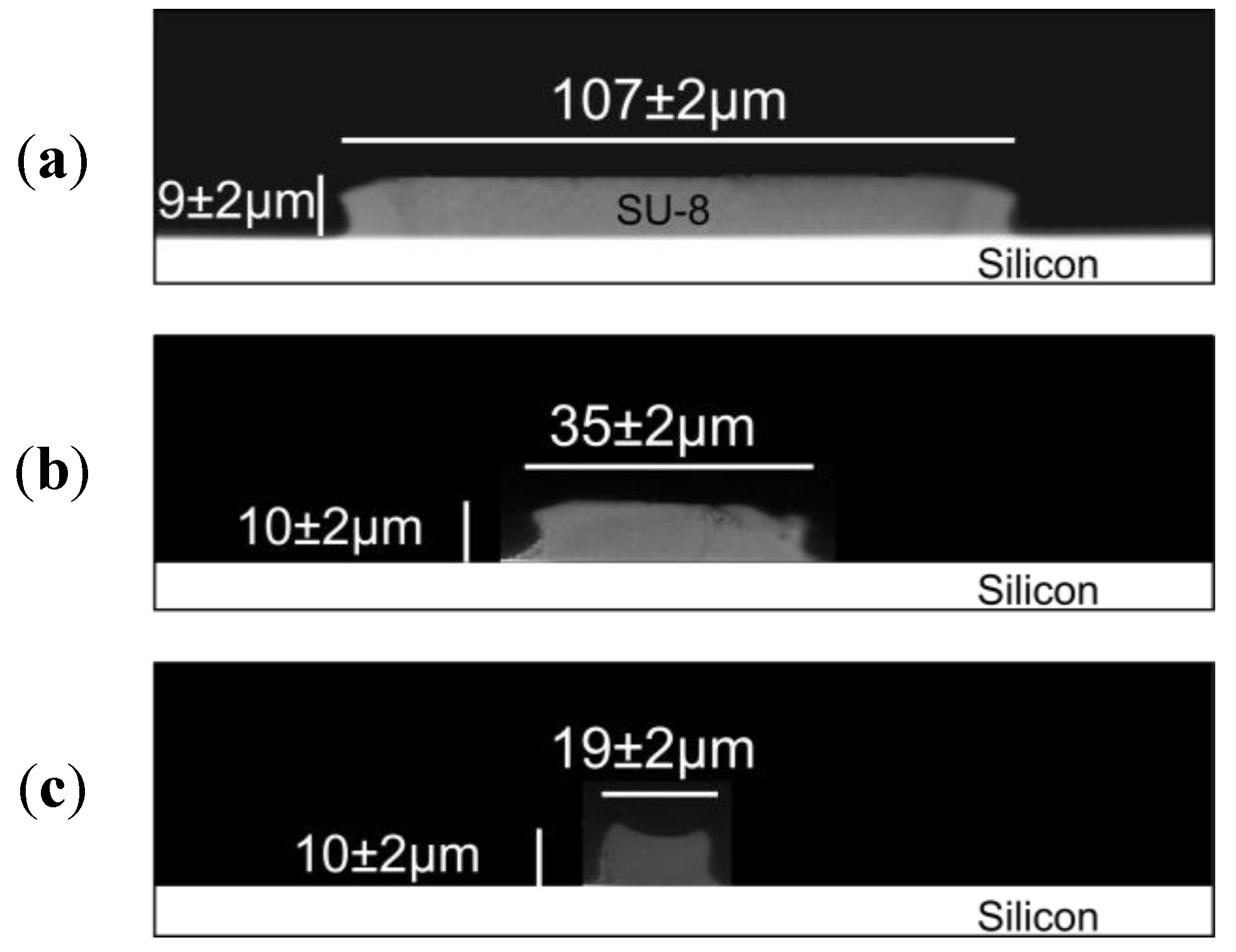
To investigate the whole three-dimensional structure of photoresist features, obtained by UV box and photographic masks, cross sections have been imaged. As can be seen in
Figure 6, the microstructures, show odd vertical walls. Microstructures represented in
Figure 6a,b with a width of 107 and 35 µm respectively have the same shape. Approaching the resolution limit, the shape changed and it became difficult to obtain straight edges. The visible fractures, especially in
Figure 6b, are due manual breaking of samples, made to investigate the microstructure sections. The realization of vertical sidewalls is not trivial and many effects, due to both instrument features and process conditions, should be considered to understand the final shape of the ridge. SU8 process conditions, mainly solvent bake, exposure dose and post exposure bake could also affect the SU8 sidewall shape. An extended discussion about SU-8 side walls has been reported by del Campo
et al. [
20]. In our opinion many additional effects must be taken into account in this case. We chose the emitting wavelength of the UV lamps (~350nm) as near as possible to designed wavelength for SU-8 (365 nm). Strong optical adsorption of SU-8 under 360 nm, does not allows homogeneous vertical exposure in thick films [
19] and unfortunately high-pass and narrow-band filters are not suitable for a large area UV box.
Figure 6.
Microscope images of microchannel cross sections with three different widths, (a) 107 µm; (b) 35 µm; (c) 19 µm, realized in SU-8 on a silicon wafer (white zone).
Figure 6.
Microscope images of microchannel cross sections with three different widths, (a) 107 µm; (b) 35 µm; (c) 19 µm, realized in SU-8 on a silicon wafer (white zone).
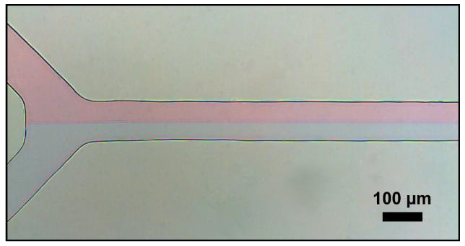
More important is that the uncollimated light provided by lamps does not hit vertically the photoresist and a collimation light system cannot be added without leaving the aim of a low cost setup. The combination of all these effects produces the wall shape irregularity imaged in the microphotograph. In any case, this shape did not cause problems to PDMS peeling off during replica molding process. In order to prove that these defects do not compromise the usefulness of the technique, a Y shaped microchannel has been realized in PDMS. Red and blue dyes were injected in the two inlets of microfluidic device realized. As shown in
Figure 7, two colored stream flow in parallel without any mixing, due to the low Reynolds number. Non-vertical sidewalls are not a problem for laminar flow since the cross section is uniform along the channel. We can conclude that there is not any turbulence induced by wall shape irregularities in the microchannel.
Figure 7.
Optical image of laminar flow in a y-shaped microchannel.
Figure 7.
Optical image of laminar flow in a y-shaped microchannel.

