1. Introduction
The microscopic particle chain is a common form of assembled particles, which is involved in the colloidal, biological, electronic, photonic, magnetic and other related research fields. It plays an important role in these fields, as it serves as a link between the nanoscale world and meso- or macroscale objects. Currently, the laboratory methods for manipulating microscopic particle chains have become crucial for developing techniques on patterning magnetic nanoparticle arrays [
1], forming regular superstructures by nanoparticles [
2], constructing strings of colloidal particles [
3,
4], and creating multicellular assemblies of cells [
5] and live celloidosome structures [
6]. In order to flexibly manipulate particle chains, various methods have been developed, including the physical methods based on electric field, geometric constraint, dipole-dipole interactions or surface roughness direction [
7], and the chemical methods based on linker molecules, oriented aggregation or non-uniform stabilizer distributions [
8].
However, these methods usually need templates, physical or chemical reaction processes involving more prefabrication, and extra techniques [
8]. Many of the created particle chains or closely linked chains are immobilized and their relative positions cannot be stably controlled. In recent years, optoelectronic tweezers (OETs, also known as optically induced dielectrophoresis) have showed the ability to parallel positioning a large number of colloidal microparticles without any template [
9,
10]. The microparticles can be trapped and driven by the dielectrophoretic (DEP) forces induced by the optical micropatterns in OET devices [
11,
12]. However, the rotation of assembled microparticle chains by OETs has rarely been investigated, and the degree of freedom for varying the postures, positions or orientations of the microparticle chains still has limitations.
In this study, the formation and rotational manipulation of microparticle chains in real time are numerically and experimentally demonstrated by using OET at appropriate frequencies and voltage. The rotating electrical field for implementing the optically induced electrorotation (OER) of particle chains is achieved in OET device since the phase of alternating current (AC) potentials are varied across the bottom surface due to the different impedance of photoconductor layer at light and dark areas. The alternating current electroosmotic (ACEO) flow can also be generated in the OET device by tuning the frequency to a special range, and ACEO flow can simultaneously be produced around the location where the chains are self-rotating, which could be regarded as an assistance for providing more degree of freedom for spatially manipulating particle chains.
2. Experimental Section
The structure of the OET device and the scheme for rotating particle chains are conceptually illustrated in
Figure 1a. The equivalent circuit of the OET device is shown in
Figure 1b. The device is composed by the upper and lower indium tin oxide (ITO) slides, photoconductive layer (hydrogenated amorphous silicon, a-Si:H) with a thickness of
ta and a relative permittivity ε
ar, and a fluidic chamber with a height of
tm and the applied AC voltages. The electrical conductivity of the photoconductor layer at unilluminated and illuminated areas are denoted as σ
al and σ
ad respectively. The microfluidic chamber contains fluidic medium with a relative permittivity ε
mr and an electrical conductivity of σ
m. The micro-particles are suspended uniformly in the fluidic chamber at the initial time. The potentials applied at the upper and lower ITO layers can be expressed by phasor as
V0e
jωt and
V0ej(ωt+π), where
j =
,
V0 is the amplitude for each voltage signal and ω is the angular frequency of the applied voltage. The photoconductive layer of OET device was fabricated by plasma-enhanced chemical vapor deposition (PECVD) and was consecutively deposited with multiple featureless layers on an ITO glass.
Figure 1.
Schematically illustration of the optoelectronic tweezers (OET) device configuration and the principle for generating rotating electric field and alternating current electroosmotic (ACEO) flows. (a) Conceptual illustration of the self-rotation and circular traveling of an entire particle chains in an OET device. The motion trajectories of the particle chain around the edge of illuminated area are indicated by dashed curve lines. (b) Device structure and mechanism for generating the rotating electric field around the border between dark and light regions. ω is the angular frequency, t is time and V0 is amplitude of alternating current (AC) voltage. The electrical double layers (EDL1 and EDL2) are formed at the interface of photoconductor and medium, and the interface of indium tin oxide (ITO) and a-Si:H, respectively. (c) Electroosmotic fluid roll formed around the border between light and dark regions. FEO, q and Et are electroosmotic force, charge of counterions and tangential electric field at interface between photoconductive layer and medium, respectively.
![Micromachines 06 01387 g001]()
The experimental platform was established by assembling commercial optics, projector and an upright microscope as shown in
Figure 2a. A Digital Micromirror Device (DMD)-based projector (XG-FX810A, Sharp Corporation, Osaka, Japan) was used as both the light source (via its 230-W, 3200-ANSI lumen dc lamp, Sharp Corporation) and the interface between DMD driver circuit and the computer. The DMD forms a light image (or called optical pattern) according to the output signal of the personal computer (PC)’s external monitor port. The optical image at the output of the projector lens was collimated, collected, reflected through the reflector at 45° to the horizontal and directed into a 10X driven lens from the lower upward. The optical image was focused by the object lens, and finally projected onto the photoconductive layer of OET chip. The optoelectronic chip was situated on the stage of a Nikon ECLIPSE (Nikon Corporation, Tokyo, Japan) upright microscope. Observations were conducted through a charge-coupled device (CCD) camera mounted at the connecting port on the top of the microscope. The signal generator connecting to the OET chip was able to generate ac signal up to 36 V
peak to peak (V
pp) via a differential output between two channels. For the OET chip, the substrate with photoconductive layer has a dimension of about 2 mm × 1.2 mm. The top ITO-glass slide assembled with the bottom substrate by spacing layer has a larger dimension of around 4 mm × 1.6 mm as shown in
Figure 2b,c.
The parameter values used in this study are ta = 1.5 μm, tm = 100 μm, εar = 8, εmr = 80, σal/σad = 1000. The polystyrene microspheres used in the experiment have a diameter of 4 μm. The microparticles suspended in the micro fluidic chamber filled with potassium chloride (KCl) aqueous solution has a conductivity of σm = 5 × 10⁻³ S/m.
Figure 2.
(a) Photograph of experiment setup for the real-time controllable OET platform. (b) Front view of the OET chip. (c) Back view of OET chip. CCD: charge-coupled device.
Figure 2.
(a) Photograph of experiment setup for the real-time controllable OET platform. (b) Front view of the OET chip. (c) Back view of OET chip. CCD: charge-coupled device.
3. Principle and Modeling
The principle of the light-dark binary image induced rotating electric field (e-field) is indicated in
Figure 1b. The a-Si:H layer has different impedances on light and dark sides, which leads to the amplitude and phase difference in the electric potentials at upper surface (
V0ejωt), photoconductive layer/medium interface in dark area (
) and light area (
). These three AC potentials can create a rotating e-field in fluidic medium around the border between light and dark regions, which will lead to self-rotating of the one-dimensional particle chains due to the interaction between the dipole moment of particle chain and rotating e-field.
According to equivalent circuit of the OET device shown in
Figure 1b, and assuming that the impedance of conjunction between the light and dark regions in the a-Si:H layers is very large indicating no current flows across the border, the potential phasor at the bottom surface of fluidic chamber denoted as Φ
i is given by:
In Equation (1), the subscript
i in voltage amplitude
Vmi and initial phase
ψi and can be replaced by “l” or “d” indicating the light or dark condition for the optical projection onto photoconductor, respectively.
ZEDL1,
ZEDL2,
Za and
Zm are impedances of the EDL1 formed at the interface of a-Si:H and KCl solution (liquid electrolyte), the EDL2 formed at the interface of ITO and a-Si:H (solid electrolyte), the photoconductor layer and the medium layer, respectively. The impedance of photoconductor per unit area at light and dark regions are respectively expressed as:
Here the
Ca (=ε
arε
0/
ta) is the capacitance of a-Si:H layer per unit area,
Ra_l=
ta/σ
al and
Ra_d=
ta/σ
ad are the resistances of illuminated and unilluminated a-Si:H layer per unit area, respectively. It is assumed that
Ca has the same value for both illuminated and unilluminated a-Si:H regions. Here, the electrical double layer (EDL1) forms at medium/a-Si:H interface due to the interfacial polarization as shown in
Figure 1b. The characteristic thickness of EDL1 (
tEDL1) can be estimated by Debye length, so:
where
kb is Boltzmann constant;
T is temperature;
z is valency of ions;
e is elementary charge. ε
0 is vacuum permittivity; ε
b is the relative permittivity of medium;
n0 is the ion density. It is presumed that the voltage drop across the EDL1 is less than the thermal voltage
kbT/
ze, so that the EDL1 can be approximately described as an capacitor expressed by
CEDL1 = ε
0ε
EDL1/
tEDL1 in terms of the electroosmosis linear theory at low-voltages [
13,
14]. ε
EDL1 is the relative permittivity for the aqueous medium inside EDL1. The
CEDL1 at light and dark areas (denoted as
CEDL1_l and
CEDL1_d) has different values mainly because of the different ε
EDL. The electrons in illuminated a-Si:H are much more abundant than those in unilluminated a-Si:H. The EDL1 has a much higher charge density on illuminated area than unilluminated area at the medium/a-Si:H interface, and thus the e-field inside EDL1 is much stronger on the illuminated area than that on unilluminated area. Consequently, the water molecules inside EDL1 within illuminated area are so highly aligned in order, which results in a lower polarization ability for aqueous medium inside it. Therefore, ε
EDL1 could have a smaller value in light area than that in dark area. Here ε
EDL1 is estimated 20 in light area and 80 in dark area. The EDL1 also exhibits resistance property during every charging period, so an equivalent resistance
REDL1 (=
tEDL1/σ
EDL1, and σ
EDL1 is the conductivity inside EDL1) in series with EDL capacitor is assumed for more accurate calculation. During the charging process, the counterions being attracted to the interfacial plane will experience repelling Coulomb force from the increasingly dense counterions already stored in EDL. Therefore, σ
EDL1 should be significantly smaller than σ
m. Here σ
EDL1 is assumed as one-hundredth of σ
m. Hence, the impedance of EDL1 at medium/a-Si:H interface per unit area at light and dark regions are respectively expressed as:
where the ε
EDL1_l and σ
EDL1_d are the relative permittivities of EDL1.
tEDL1 could have the same value at both light and dark areas since it is mainly determined by the property of bulk medium (ε
0,
z,
n0) as presented in Equation (4) and not dependent on the electrical property of photoconductor. In this study,
T = 293 K,
kb = 1.3806503 × 10
−23 J·K
−1, ε
0 = 8.8541878 × 10
−12 F·m
−1,
e = 1.602176462 × 10
−19 C;
z2 = 1;
n0 = 3.011 × 10
23 m
−3 (5 × 10
−4 M KCl solution). According to Equation (4), the characteristic thickness of EDL1 (
tEDL1) is calculated to be 13.6 nm.
Similarly, the impedance of EDL2 could be calculated through the assumed expression with the form [
15,
16]:
where
at ω = 1 rad/s,
P is a constant between 0 and 1. The
ZEDL2 is constant phase angle impedance. Here, the thickness
tEDL2 for EDL2 is assumed around 5 nm in dark a-Si:H and 0.5 nm in light a-Si:H, since the concentration of charge carrier is higher in light a-Si:H and thus only a thinner double layer of counter charges is required to electrically balance the surface charge of ITO layer. The conductivity σ
EDL2 inside EDL2 for dark and light region is assumed as one-tenth of σ
al and σ
ad. The permittivity ε
EDL2 = 8ε
0,
P = 0.7 in this calculation.
The phase angles and amplitude for the AC potentials on the bottom of fluidic chamber in
Figure 1b can be calculated as
ψd = 0.577,
ψl = 3.35,
Vmd = 3.16 and
Vml = 3.10 at 700 kHz. Thus, three potentials creating the rotating e-field can be written as 5
ejωt, 3.16
ej(ωt + 0.577) and 3.10
ej(ωt + 3.35) respectively. The noticeable phase difference exists from 50 kHz to 4 MHz according to the calculation, so the electrorotation could be achieved within a wide range of frequency.
When a microparticle chain is self-assembled under an e-field
E with appropriate strength, a polarization would be induced in the particle chain. The effective dipole formation of the entire particle chain (the effective dipole moment is denoted as
Pc) has a time delay behind establishment of the field
E, since it takes a finite amount of time for the dipole moment to become aligned with the field vector. When the e-field
E rotates, the
Pc follows it and rotates with a phase lag. The particle chain undergoes a rotational torque as [
17,
18]:
where
is the complex phasor of the effective dipole moment of a particle chain,
is conjugated complex phasor of the e-field exerting on particle chains, Re[...] and Im[...] indicate the real part and imaginary part, and
v is the volume of a single particle. β is the effective polarisability of a particle chain and will increase with rising particle number. The effective longitudinal and transverse polarisability of particle chains can be mathematically expressed as the function of polarisability of a single particle and the relative polarisability described by polylogarithm of the scaled dielectric constant [
19].
k is the modification coefficient for compensating the distortion of electric field due to presence of the particle chain. Here
is denoted as characterization factor for the rotating field.
In addition to the torque acting on particle chains, the nonuniformity of electric field also induces dielectrophoretic (DEP) force probably driving particles and particle chains to move transnationally (not rotationally). According to electrokinetic theory, the time-averaged DEP force acting on particles can be expressed as [
16]:
where
is the complex phasor of the effective dipole moment of a particle,
is nabla operator or called vector differential operator,
v is the volume of particle,
is the complex phasor of electric field and
is the effective polarisability of a particle, expressed as
.
is referred to as the Clausius-Mossotti (CM) factor. ε
m is the permittivity of fluidic medium.
and
are the complex permittivities of particle and fluidic medium respectively.
The microparticle chains do not only undergo electrorotation torque and DEP force, but could also be influenced by the optically induced ACEO flows induced. ACEO flow is the motion of fluid due to an interaction between an e-field and the EDL1 induced at medium/a-Si:H interface as shown in
Figure 1c. Here, the dark area of a-Si:H also generates electron-hole pairs because of background illumination, so EDL1 is also formed in dark area. The EDL1 within the illuminated area has higher charge density than that within the dark area, and the tangential e-field mainly arises around the edges of optical micropatterns. Therefore, the ACEO flow mainly occurs around the optical micropatterns projected on the photoconductive layer. ACEO flow can let the particle chains travel in a nearly circular trajectory as shown in
Figure 1c. After applying the voltages, counterions accumulate in the EDL1area. Due to the distortion of electrical field induced by the optical virtual electrode (optical micropattern), a tangential component of e-field arises round the medium/a-Si:H interface. As a result, the ions in EDL1 are subjected to the tangential electrostatic force along the horizontal direction. This force is then transmitted to the fluid via viscous friction and drives the boundary liquid to flow at a slip time-averaged velocity that can be calculated by using the Helmholtz-Smoluchowski equation [
20,
21]:
where
φ is the potential phasor just outside the EDL1,
φS is the potential at the nonslip-plane close to the solid surface of the EDL1.
is the conjugated complex phasor of the tangential e-field just outside the EDL1. ε
mr is the relative permittivity of medium. η is dynamic viscosity of the solution. η = 1 × 10
−3 Pa·s for aqueous medium. According to the basic capacitor-resister model of EDL [
20], the optimal charging time is approximately of order of τ
c = (ε
EDL1_lε
0/σ
m)(
tm/λ
D), where
tm is the gap spacing between upper ITO layer and a-Si:H layer (
tm = 100 μm in this study) and ε
EDL1_l/λ
D is the proximate characteristic capacitance of the EDL1. When the frequency is very low (ω is far smaller than 1/τ
c), the EDL1 can completely form, and the majority of applied voltage is dropped across the EDL1, which leads to a moderate magnitude of |
φ −
φS|, but the tangential e-field (
) just out of the EDL1 tends to zero. Contrarily, when the frequency is very high (ω is far larger than 1/τc), there is not adequate time to form a completely charged EDL1, and most of the applied voltage is dropped across the bulk medium getting the magnitude of |
φ −
φS| reduced to almost zero, although a stronger tangential e-field (
) at the outer region of EDL1 is available. Therefore, the much higher or much lower frequencies will make the boundary slip velocity cease.
The electrorotation of particle chains can dominate at frequencies above 600 kHz because the ACEO-induced particle chain rotation is weakened significantly at higher frequencies above around 700 kHz. Appropriately, tuning down the frequency can make the ACEO flow available and then assist the self-rotating particle chains to travel along circled trajectory.
4. Simulation and Analysis of Electric Field and Flow Pattern
The rotating e-field was numerically simulated using a commercial finite element program (COMSOL Multiphysics, AC/DC Module, COMSOL Inc., Stockholm, Sweden) based on the physical model and the principle elucidation for the rotation of e-field induced by phase differences of potentials around inner boundary of fluid chamber shown in
Figure 1. Considering the typical applied electric field frequency and the characteristic time scale in this study, the effect of electrorotation and ACEO can be described as a combination of a quasi-electrostatic and a flow problem. Thus, the modules for quasi-static electric field and incompressible Navier-Stokes fluid were employed in the COMSOL program. The fluid domain is filled with KCl solution, so it can be regarded as a homogeneous linear dielectric with permittivity σ
m and conductivity ε
m, and the governing equation for electric potential distribution is:
where
is the potential phasor needs to be solved. To obtain the distribution of flow velocity, the incompressible Navier-Stokes equations as shown below should be solved:
where
u is velocity field and
p is the pressure. The ACEO only induced slip fluid velocity on the boundary and does not induce body force. For the time-averaged velocity in fluid domain, the external force
F in Equation (12) should be zero. As shown in
Figure 3, the boundary condition for calculating the variation of e-field distribution within time domain (
Figure 3a), the time-averaged e-field (
Figure 3b) and the micro flow pattern (
Figure 3c) are presented. It is assumed that no current flows across the boundary between the illuminated and unilluminated regions in the a-Si:H layer because the impedance of conjunction is very large [
22].The upper surface of EDL1 was set as bottom boundary surface of the computation domain for calculating the term
in Equation (10). The EDL1 in the light and dark area was modeled by the boundary condition
(it can also be equivalently expressed by another mathematical form of distributed impedance in COMSOL program), where σ
m is the electrical conductivity of the bulk medium,
φ is the potential phasor needing to be solved at the bottom boundary of fluidic chamber.
z is the vertical coordinate. In above boundary expression,
R =
tEDL1/σ
EDL1 and
X = −1/(ωC
EDL1_
i), and the subscript
i can be replaced by “l” or “d” indicating the light or dark condition respectively due to the optical projection onto photoconductor. Firstly, the distribution of the slipping rate of boundary liquid just out of EDL1 was simulated according to Equation (10) in the module for quasi-static electric field. Then, this slipping rate distribution on the bottom surface was used as a boundary condition of fluidic velocity for simulating the incompressible Navier-Stokes fluid flow.
Figure 3.
(a) Boundary condition for the simulating the transient distribution of quasi-static rotating e-field. φ(t) is the time-dependent electric potential. (b) Boundary condition for simulating the distribution of the time-averaged physical quantities of rotating e-field. φ is the complex phasor of the electric potential. J is the current density and n is the unit vector normal to the boundary. (c) Boundary condition for computing the distribution of fluidic velocity. p is the pressure; n is unit normal vector; u and v are horizontal and vertical components of the fluid velocity. ud and ul are the tangential ACEO slip velocity over the surface of light and dark area, respectively.
The e-field
E rotates at every position point around the light-dark border area as shown in
Figure 4a–h. The direction and magnitude distribution of
E changes over time within every signal period. However, the rotational rate of
E is not a constant. For a single particle, the induced dipole moment (denoted as
p) tends to align with the field
E, but always has a phase lag behind the rotating
E as illustrated in
Figure 4i. The distribution of characterization factor for the rotating field is presented in
Figure 4j, which indicates the non-uniform distribution of rotation rate. The particles also undergo the DEP force (refer to Equation (9)) proportional to the
whose direction and magnitude distribution of are presented in
Figure 4k. The particles tend to move to the location indicated by the frame in
Figure 4k, which is the location for rotating particles or particle chains.
Figure 5a shows how the dispersed particles formed a one-dimensional chain well aligned by using simulation results and schematic elucidation. At initial time
t = (0.19 +
n1)
T, an effective dipole moment
p would be induced in every microparticles under the effect of an e-field
E, and the dispersed microparticles tends to gradually assemble into an one-dimensional structure in an intermediate process lasting for many signal periods (refer to
Figure 5a). The inter-attraction of adjacent particles is mainly because the attractive DEP force exists between adjacent particles under the oriented e-field in local region [
23]. The presence of particles distorts the e-field around the particles, which creates a negative dielectrophoretic force that moves the particles toward the lower electric field region in the gap between particles, and thus adjacent particles attract each other. On the other hand, particles experience both translational and rotational motion with respect to each other during the chain formation process (as illustrated in
Figure 5a). In case of rotational motion, particles can rotate clockwise or counterclockwise in the other to obtain the shortest path for parallel alignment with the electric field [
23,
24]. At
t = (0.6 +
n4)
T, the particle chain formed. The fast rotating e-field and slow rotating particle chain are illustrated in
Figure 5b. The e-field
E rotates at every position point around the light-dark border area, and the induced dipole moment of an entire particle chain (denoted as
Pc) continuously tries to align with the rotating field
E, nevertheless there exists a phase lag between the
Pc and
E. Therefore, the particle chain as an entire object undergoes a rotational torque due to the electrorotation mechanism. The interactions between the polarized particle chain and the rotating e-field at different instants are also graphically demonstrated in
Figure 5c, particle chain rotates at a much lower rate relative to the fast rotating-field. In another word, the particle chain exhibits only less than half cycle of rotary movement after thousands of rotation cycles of e-field, as shown in
Figure 5c. In the rotating process, the torque on particle chain (
Γ) always keeps unidirectional.
Figure 4.
Numerical simulation results for the rotating electric field inside OET chip. (a–h) Distributions of the directions (arrows) and magnitudes (surface plot) of electric field at different time instants. (i) Schematically illustration of the phase lag between effective dipole moment p of a single particle and rotating e-field strength E. (j) Distribution of the characterization factor of rotating field. T denotes the period of applied AC signal. ω1, ω2, and ω3 are the rotation rates. The size of simulation domain is set as 60 μm (width) × 100 μm (height) in (a–h) and 70 μm (width) × 100 μm (height) in (j–k). The width of light region is kept as 30 μm. The amplitude and frequency are set V0 = 5 V and 700 kHz respectively.
Figure 5.
Analysis for particle chain formation and rotation based on the numerical simulation results of the rotating electric field. (a) Illustration and analysis of the process for particle chain formation. It includes rotational and translational motion of surrounding particles relative to the central of this structure. (b) Elucidation of the interaction between the polarized particle chain and the rotating vector E. (c) Illustration of the rotation of particle chain relative to its geometry center in rotating e-field at different time instants. n1, n2, n3, n4 are integers and indicate the different number of signal cycles that the particles experienced. T denotes the period of applied AC signal. The size of simulation domain is set 60 μm (width) × 100 μm (height), and the width of light region is set 30 μm. The amplitude and frequency are set 5 V and 700 kHz respectively.
As shown in
Figure 6a, the two potentials at the lower layer of EDL1 in light (denoted as
Vl) and dark (denoted as
Vd) areas are phase-shifted with different extents compared to that at the top ITO layer. It makes the polarities of
Vl and
Vd can exchange over time within one period. For example,
Vl is negative and
Vd is positive at
t = 0.1
T, while
Vl becomes positive and
Vd becomes negative at
t = 0.3
T. These two cases are simulated and analyzed in
Figure 6b,c. Here, the dark area of a-Si:H still has electron-hole pairs because of background illumination, so EDL1 is also formed in dark area. The simulated e-field indicates that
E attenuates with the increased height from the fluid chamber bottom and the strongest
E exists close to the border of the light and dark regions. The slip flow rates just outside the upper boundary of EDL1 at light and dark areas are denoted as
ul and
ud respectively.
ul and
ud are found to be in opposite directions according to the polarities of
Vl and
Vd over time. Based on the simulation results of e-field and the expression of instantaneous electroosmotic (EO) flow velocity
uEO = ε
mrε
0Λ(φ − V
i)
Et/η (φ is the potential just outside the EDL,
Vi could be
Vl or
Vd,
Et is the tangential e-field strength and Λ is the ratio of the voltage across the slipping part of EDL to the voltage across the whole EDL), it is found that |
ul| > |
ud| at
t = 0.1
T (
Figure 6b), while |
ul| < |
ud| at
t = 0.3
T (
Figure 6c). Therefore, the net velocity
uEO is in positive direction at
t = 0.1
T (
Figure 6b) while in negative direction at
t = 0.3
T (
Figure 6c). It is followed that the direction of the time-averaged ACEO flow velocity on the slip boundary depends on the integral of
uEO over time. It is reasonable that the ACEO fluid roll changes direction from positive to negative if the negative
uEO is enhanced or positive
uEO is weakened.
Figure 6.
(a) Optically induced electric potentials at the lower layer of EDL1 (light and dark areas) and top ITO layer. (b) Electric field distribution in fluid chamber at t = 0.1T. (c) Electric field distribution in fluid chamber at t = 0.3T. T is the period of AC voltage. (d) Simulation result of the optically induced ACEO flow pattern. (e) ACEO flow velocity field around the border of the light (right side) and dark (left side) area of EDL1. (f) Tangential fluid velocity distribution along the horizontal coordinate at the height of 3 μm.
In this study, a larger voltage (tens of times higher than the thermal threshold (~25 mV) is applied in order to construct long particle chains. This would cause the EDL1 to overcharge and thus the ions with finite-size (which cannot be simply regarded as points any more) are crowdedly packed on the interface, which is called the steric effect of the finite-sized ions inside the DEL1 [
25]. Inside the EDL1 within light area, the crowded ions (hydrated ions) with finite sizes will lead to a condensed layer whose thickness grows with increased voltage, resulting in growing viscosity of the condensed layer, and thus the ACEO mobility will gradually saturate with increased voltages [
26,
27]. In contrast, the EDL1 within dark area stores much less ions and could not form a condensed layer of ions, since the carriers of electron-holes in dark EDL1 keep approximately 10
3 times lower concentration than that in light EDL1. Hence, with the increased voltage within large value ranges (e.g. from 10 to 20 V
pp), the ACEO mobility of dark EDL1 has been increased to higher value; while the ACEO mobility of light EDL1 have much smaller increment due to its enhanced viscosity. Consequently, the net ACEO slipping flow of EDL1 is in negative direction. The simulation results of flow pattern are shown in
Figure 6d–f by incorporating the enhanced viscosity of EDL1 in light area. The fluid roll in clockwise direction (
Figure 6d) is different from the traditional ACEO flow generated by asymmetrical metal-electrode pairs [
28,
29]. The detailed flow velocity field close to the border of light/dark area is presented as
Figure 6e: there are two fluid vortices located at the left-side and right-side respectively around the border of light/dark area. The left-side vortex (clockwise) is stronger than the right-side vortex (counterclockwise). As shown in
Figure 6f, the tangential fluid velocity varies with horizontal position at the height of 3 μm, and the integral of negative velocity is larger than the integral of positive velocity over the horizontal coordinates. Therefore, the resultant fluid field is like a vortex in clockwise direction and it spans the overwhelming majority of fluid chamber. Additionally, the ACEO flow rate varies along each circled streamline, which will result in the travelling of particle chains with nonuniform speed in ACEO flow roll.
5. Experimental Results
In the experiment, the polystyrene microparticles with a diameter of 4 μm self-assembled into chains within the fluidic medium when appropriate voltage was applied across the upper and lower ITO layers. The motion of particle chains can be enhanced with the increased voltage. The self-rotation of particle chain around the middle point of chain inside fluidic medium was demonstrated by applying an AC voltage of 20 V
pp and 700 kHz to the OET chip (
Figure 7a). In this case, the electrorotation effect dominates the motion of particle chains since the ACEO-induced particle chain rotation is relatively weak at frequencies higher than 700 kHz. As shown in
Figure 7b, the two ends of particle chains exchanged after around 2.8 s (frames from 0.8 to 3.6 s) and had completed the first half-cycle of self-rotation. Then, the particle chains continued to self-rotate through the other half-cycle taking only around 1.6 s (frames from 3.6 to 5.2 s). Therefore, the rotation rate of particle chain was not a constant, and it varied with time in every period. During the whole period, there is only small displacement of particle chain away from the edge of optical pattern. An experimental video for the rotation of particles chains and single particles at 700 kHz can be found in the
supplementary information.
The particle chains also exhibited a circular traveling around the center of fluid roll generated by the optically induced ACEO effect at frequencies below 700 kHz. As indicated in
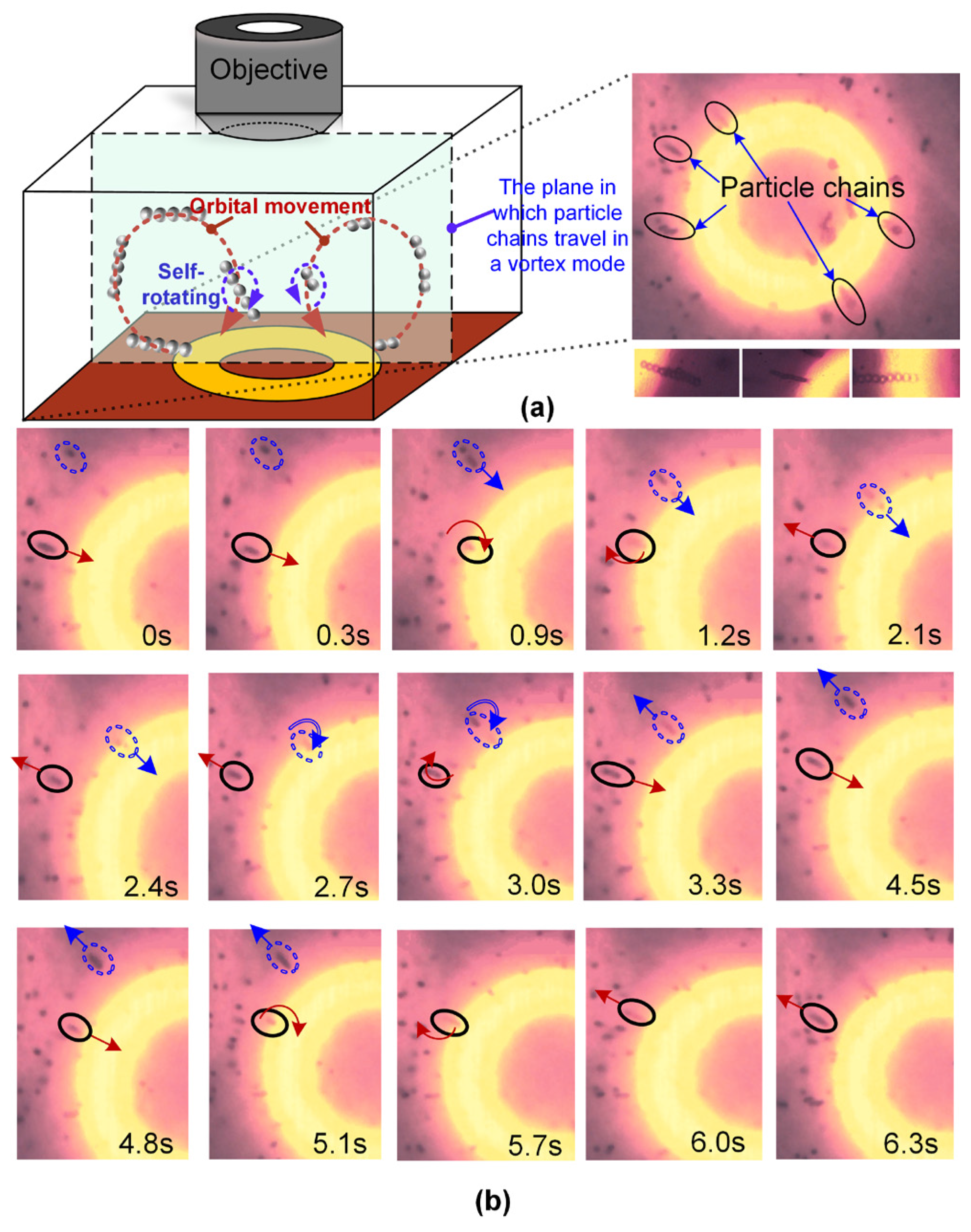
Figure 8a, the ACEO flow assisted rotation of particle chains consisted of two component motions: the self-rotation and orbital movement of the entire particle chain. The right half of
Figure 8a shows the optically projected ring-shaped micropattern and the formed microparticle chains around the optical ring. The ACEO flow assisted rotation of microparticle chains at 480 kHz are shown in
Figure 8b. The particle chains were moving closer to the edge of optical pattern, and turned around within vertical planes after a short time(less than one second or a few seconds). Then, the particle chains were moving away from the optical ring. They continued to turn around at the other side of the circular path, and then moved closer to optical ring. The orbital moving of particle chains was not uniform motion, and the vertical plane in which the circularly orbital movement occurred is approximate normal to the horizontal plane on which optical ring is projected, which exhibits more degree of freedom for the three-dimensional (3D) movement of distributed particle chains.
Figure 7.
Self-rotation of chains of particles with a diameter of 4 μm in their pitch axes by the rotating electric field at 700 kHz. (a) Schematic description of the self-rotation of a chain of particles in OET device. (b) Experimental snapshots of movement of particle chains at a series of time instants. The time unit is second (s).
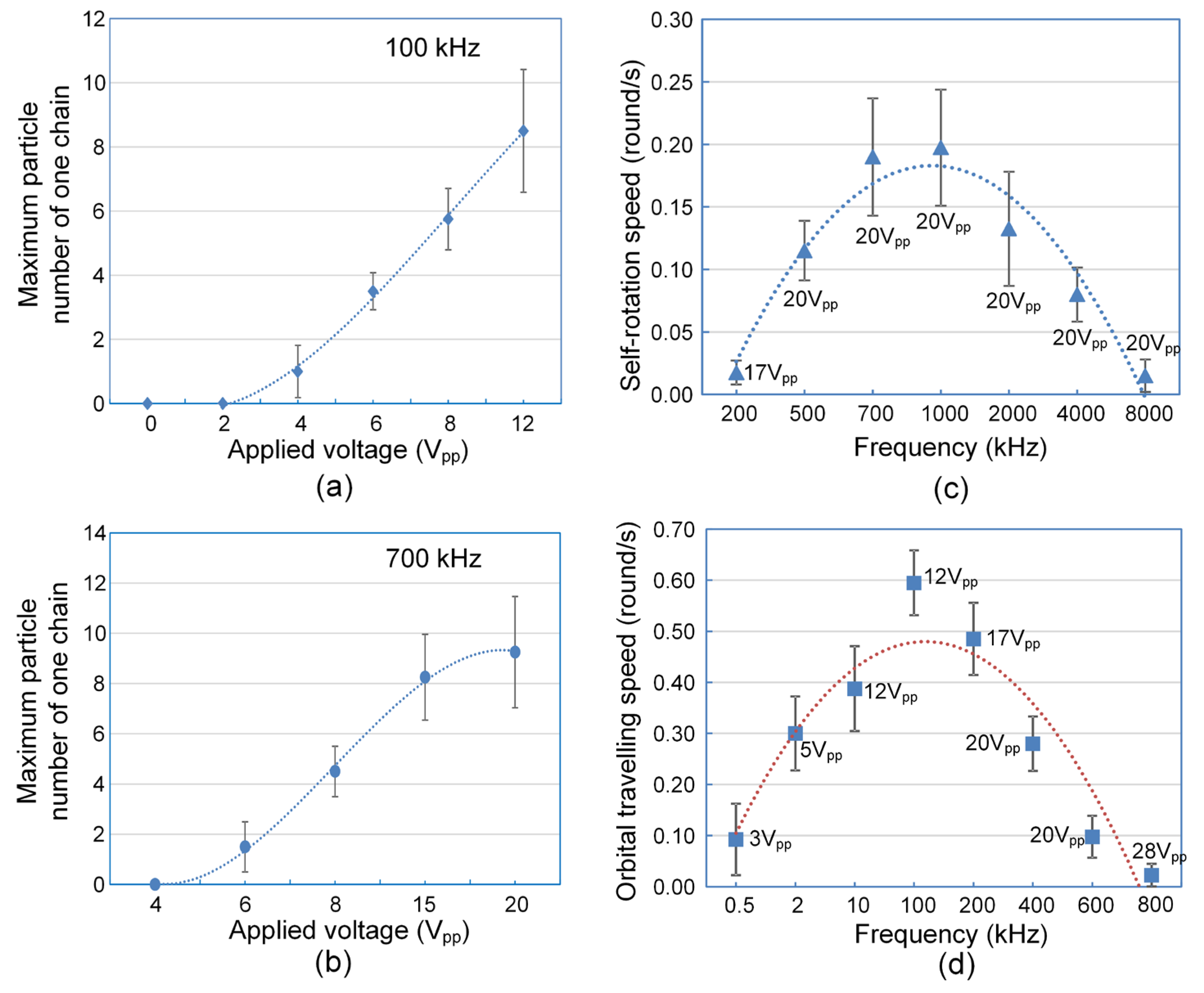
The quantitative study on the experiments are performed by measuring the dependence of particle chain length on the applied voltage, dependence of self-rotating and orbital travelling speeds of particle chains on the signal frequency and the motion process in one period of self-rotation of particle chains. The obtained results are shown in
Figure 9. In the OET chip illuminated by light patterns, the maximum length of particle chain length is related to the applied voltage, which can be characterized by dependence of the maximum particle number of one particle chain on the applied voltage as shown in
Figure 9a,b. Particle chains consisting of more than one particles can be observed above 4 V
pp at 100 kHz, and the chain length increases with voltage rise until the applied voltage reaches 12–15 V
pp (larger voltage causes bubbles due to hydrolysis). The particle chains start to form above 6 V
pp at 700 kHz, and the length of particle chains increases with voltage until 20 V
pp. As shown in
Figure 9c, the self-rotation speed of particle chains increases with the frequency rise, reaches the maximum at around 1 MHz, then decreases with further frequency rise, and could be neglected above 8 MHz. During one period of self-rotation, the speed of particle chain is not a constant and the non-uniform intermediate process for self-rotation depends on the non-uniformity of the polarized rotating e-field, which is caused by the three stimulating potentials with different amplitude of
V0,
Vml and
Vmd and non-equally shifted phases (0,
φl,
φd) as indicated in
Figure 1b. The circularly orbital movement of particle chains in three-dimensional (3D) space also sensitive to the applied frequency as presented in
Figure 9d. To avoid any hydrolysis effect and meanwhile obtain higher rotation speeds, voltages from 3 to 28 V
pp are employed for different frequency ranges.
Figure 9d presents the practically achievable speeds of orbital movement (ACEO flow rate) sensitive to the frequency, which could be utilized to guide and control the complex motion of ACEO-assisted circled travelling of particle chains. These results exhibit more degrees of freedom for adjusting the 3D movement and distribution of particle chains by varying the voltage, frequency and motional time. They offer more approaches for spatially controlling the posture, orientation or rotation speed of particle chains for applications in the field of electrics, mechanics, optics and biodevices.
Figure 8.
Optically induced ACEO flow assisted rotation of self-assembled microparticle chains at AC voltage of 20 Vpp and 480 kHz. (a) Schematic description of the resultant motion consisting of self-rotation and orbital movement of particle chains in OET device. (b) Experimental snapshots of movement of particle chains at a series of time instants. The microparticles have a diameter of 4 μm. Arrows indicate the directions of orbital movements of particle chains in each snapshot. The time unit is second (s).
Figure 9.
The quantitative study on the particle chain length, self-rotation and orbital movement of microparticle chains. (a–b) Dependence of the maximum particle number of self-assembled particle chain on the applied voltage at 100 and 700 kHz. (c) Dependence of self-rotation speed of particle chain on the frequency. (d) Dependence of orbital movement speed of particle chains on the frequency. The applied voltages are smaller at lower frequencies for avoiding hydrolysis. The microparticles in these measurements have a diameter of 4 μm. The data points in each figure are fitted by second-order polynomial curves.


