Fabrication and Actuation of an Electrowetting Droplet Array on a Flexible Substrate

Abstract
:1. Introduction
1.1. Background
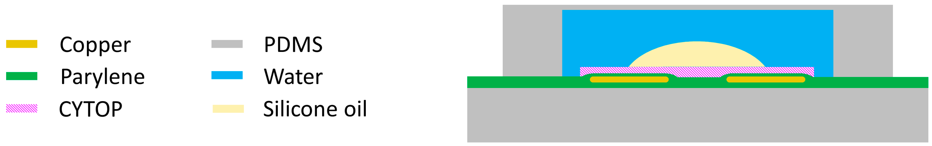
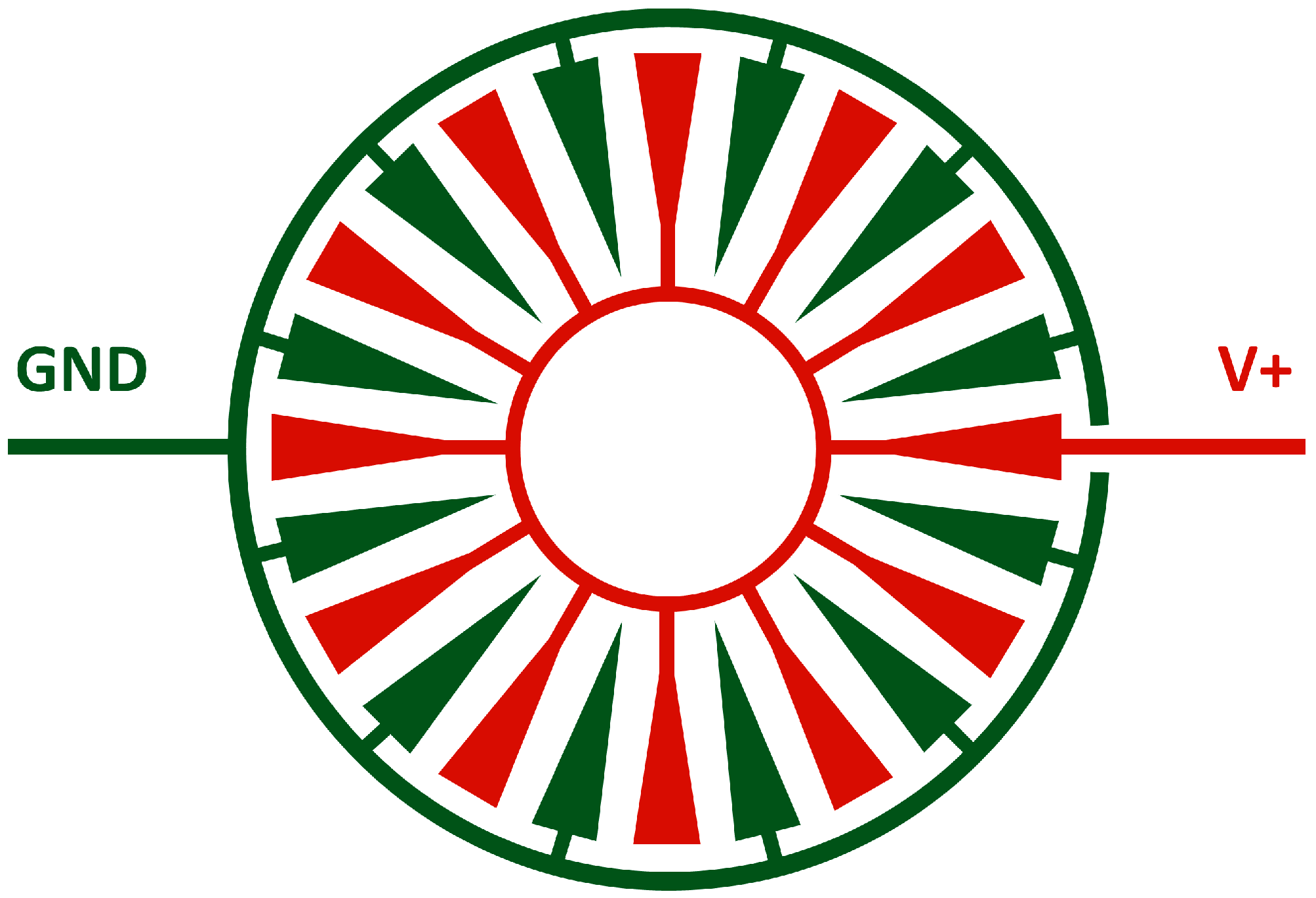
1.2. Concept and Acutation Mechanism
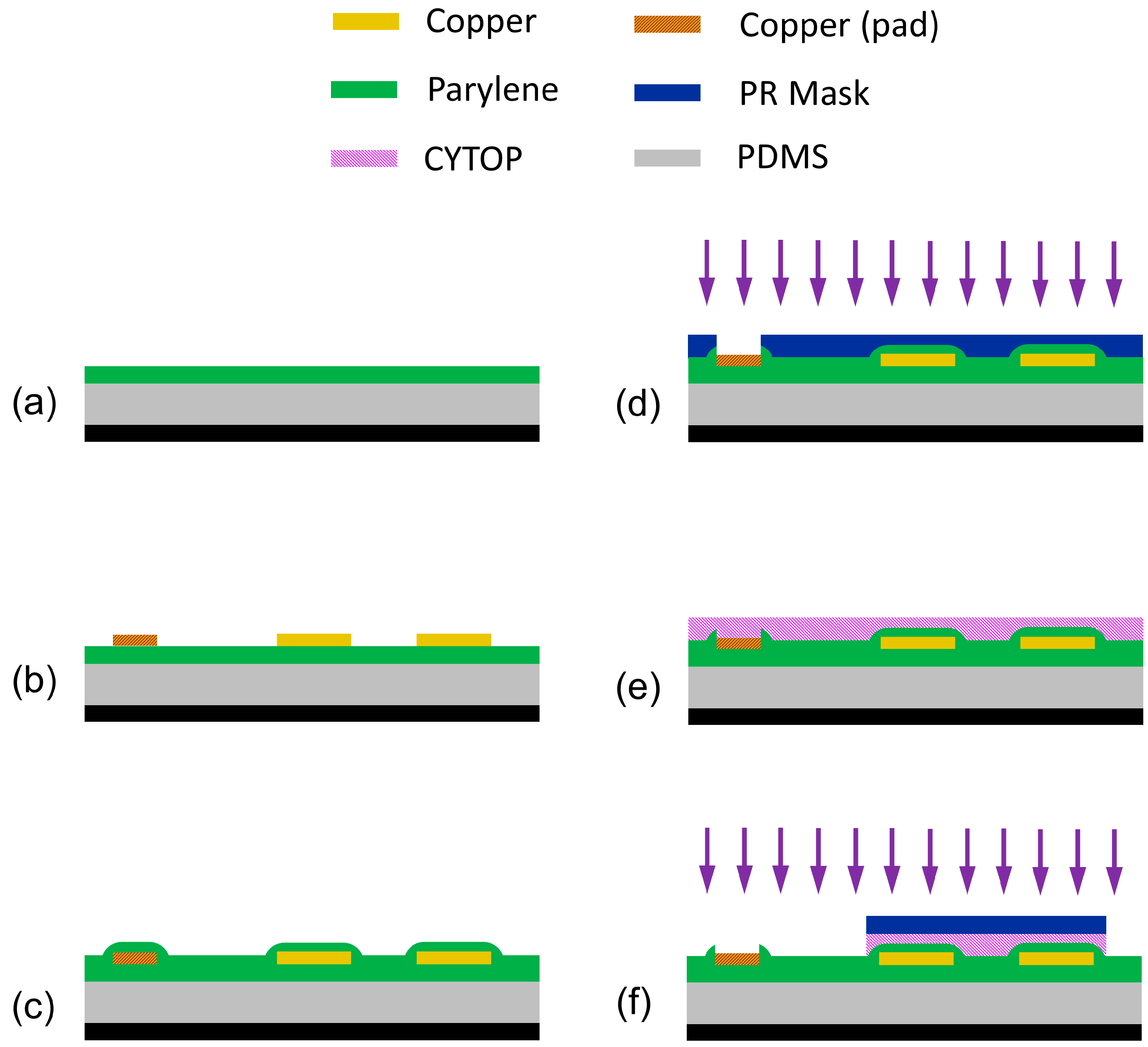
2. Materials and Methods
3. Results
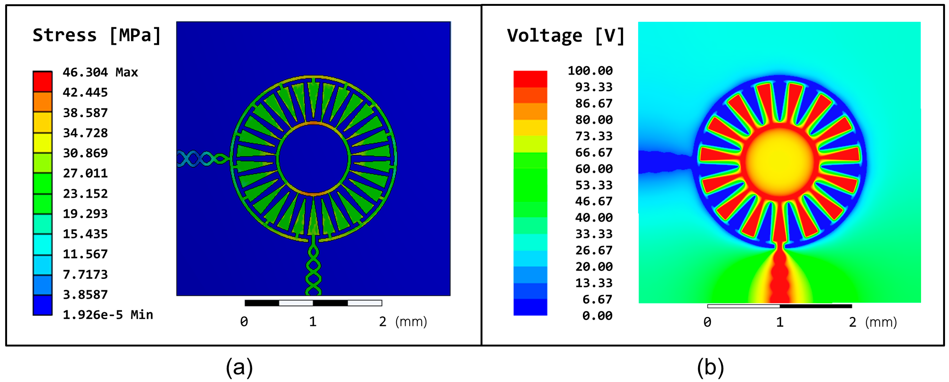
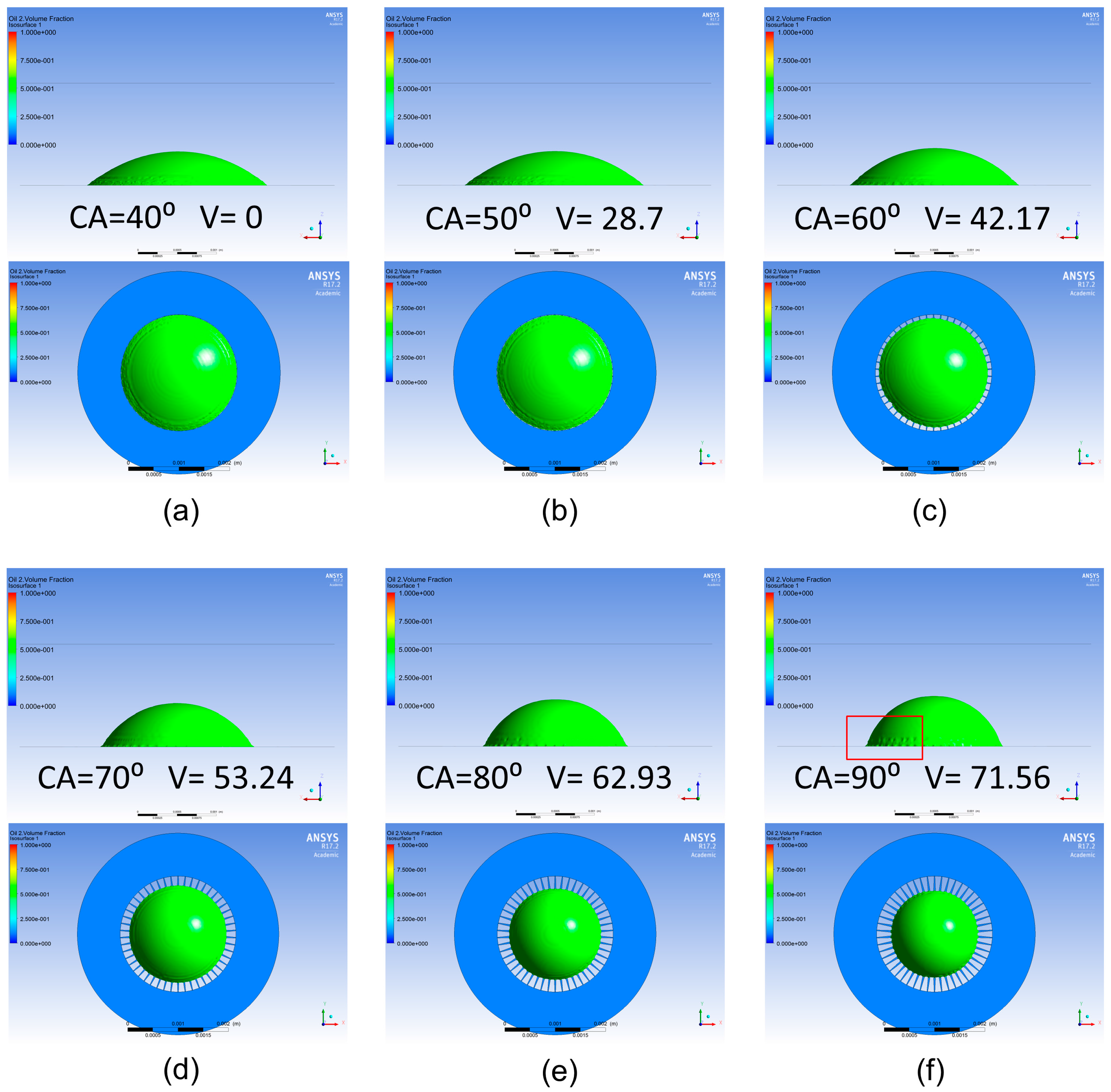
3.1. Simulation
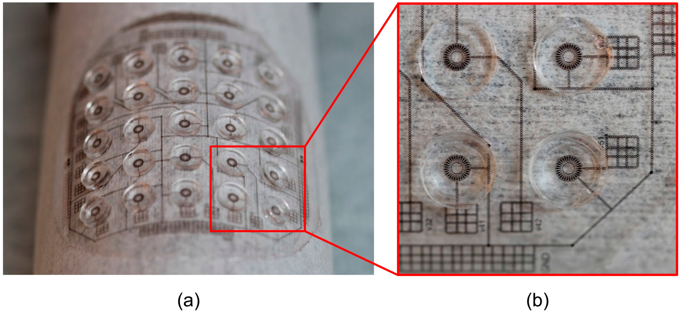
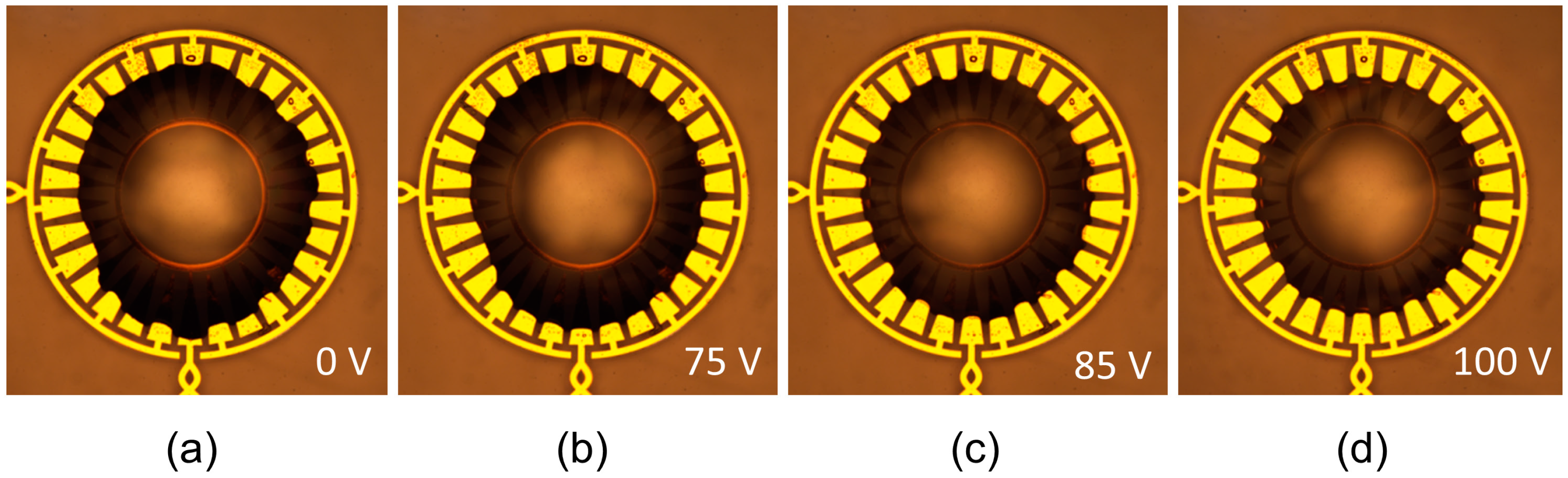
3.2. Experimental Results
4. Discussion and Conclusions
Acknowledgments
Author Contributions
Conflicts of Interest
References
- Shields, C.W., IV; Reyes, C.D.; López, G.P. Microfluidic cell sorting: A review of the advances in the separation of cells from debulking to rare cell isolation. Lab Chip 2015, 15, 1230–1249. [Google Scholar] [CrossRef] [PubMed]
- Pollack, M.G.; Shenderov, A.D.; Fair, R.B. Electrowetting-based actuation of droplets for integrated microfluidics. Lab Chip 2002, 2, 96–101. [Google Scholar] [CrossRef] [PubMed]
- Paik, P.; Pamula, V.K.; Pollack, M.G.; Fair, R.B. Electrowetting-based droplet mixers for microfluidic systems. Lab Chip 2003, 3, 28–33. [Google Scholar] [CrossRef] [PubMed]
- Cho, S.K.; Moon, H.; Kim, C. Creating, Transporting, Cutting, and Merging Liquid Droplets by Electrowetting-Based Actuation for Digital Microfluidic Circuits. J. Microelectromech. Syst. 2003, 12, 70–80. [Google Scholar] [CrossRef]
- Jones, T.B.; Fowler, J.D.; Chang, Y.S.; Kim, C.J. Frequency-based relationship of electrowetting and dielectrophoretic liquid microactuation. Langmuir 2003, 19, 7646–7651. [Google Scholar] [CrossRef]
- Li, C.; Jiang, H. Electrowetting-driven variable-focus microlens on flexible surfaces. Appl. Phys. Lett. 2012, 100. [Google Scholar] [CrossRef] [PubMed]
- Fan, S.; Huang, P.; Wang, T.; Peng, Y. Cross-scale electric manipulations of cells and droplets by frequency-modulated dielectrophoresis and electrowetting. Lab Chip 2008, 8, 1325–1331. [Google Scholar] [CrossRef] [PubMed]
- Wang, H.; Dembo, M.; Wang, Y. Substrate flexibility regulates growth and apoptosis of normal but not transformed cells. Am. J. Physiol. Cell Physiol. 2000, 279, 1345–1350. [Google Scholar]
- Steckl, A.J.; You, H.; Kim, D. Flexible electrowetting and electrowetting on flexible substrates. Proc. SPIE 2011, 7956, 1–6. [Google Scholar] [CrossRef]
- Fan, S.; Yang, H.; Hsu, W. Droplet-on-a-wristband : Chip-to-chip digital microfluidic interfaces between replaceable and flexible electrowetting modules. Lab Chip 2011, 11, 343–347. [Google Scholar] [CrossRef] [PubMed]
- Lu, Y.S.; Tu, H.; Xu, Y.; Jiang, H. Tunable dielectric liquid lens on flexible substrate. Appl. Phys. Lett. 2013, 103, 261113. [Google Scholar] [CrossRef] [PubMed]
- Murade, C.U.; Oh, J.M.; van den Ende, D.; Mugele, F. Electrowetting driven optical switch and tunable aperture. Opt. Express 2011, 19, 15525–15531. [Google Scholar] [CrossRef] [PubMed]
- Ren, H.; Xu, S.; Ren, D.; Wu, S.-T. Novel optical switch with a reconfigurable dielectric liquid droplet. Opt. Express 2011, 19, 1985–1990. [Google Scholar] [CrossRef] [PubMed]
- Ashtiani, A.O.; Jiang, H. Design and fabrication of an electrohydrodynamically actuated microlens with areal density modulated electrodes. J. Micromech. Microeng. 2016, 26, 15004. [Google Scholar] [CrossRef]
- Li, C.; Jiang, H. Fabrication and characterization of flexible electrowetting on dielectrics (EWOD) microlens. Micromachines 2014, 5, 432–441. [Google Scholar] [CrossRef] [PubMed]
- Schultz, A.; Chevalliot, S.; Kuiper, S.; Heikenfeld, J. Detailed analysis of defect reduction in electrowetting dielectrics through a two-layer “barrier” approach. Thin Solid Films 2013, 534, 348–355. [Google Scholar] [CrossRef]
- Asiri, H. Fabrication of Surface Plasmon Biosensors in CYTOP; University of Ottawa: Ottawa, ON, Canada, 2012. [Google Scholar]
- Liu, C.; Park, J.; Choi, J. A planar lens based on the electrowetting of two immiscible liquids. J. Micromech. Microeng. 2008, 18. [Google Scholar] [CrossRef]
- Than, P.; Preziosi, L.; Joseph, D.D.; Arney, M. Measurement of Interfacial Tension between Immiscible Liquids with the Spinning Rod Tensiometer. J. Colloid Interface Sci. 1988, 124, 552–559. [Google Scholar] [CrossRef]
- Khodayari, M.; Carballo, J.; Crane, N.B. A material system for reliable low voltage anodic electrowetting. Mater. Lett. 2012, 69, 96–99. [Google Scholar] [CrossRef]
- Berry, S.; Kedzierski, J.; Abedian, B. Irreversible Electrowetting on Thin Fluropolymer Films. Langmuir 2007, 23, 12429–12435. [Google Scholar] [CrossRef] [PubMed]


| Materials | Young’s Modulus (MPa) | Poisson’s Ratio |
|---|---|---|
| Copper | 1.1 × 10⁵ | 0.343 |
| CYTOP | 1500 | 0.42 |
| Parylene C | 2758 | 0.4 |
| PDMS | 0.5 | 0.48 |
© 2017 by the authors. Licensee MDPI, Basel, Switzerland. This article is an open access article distributed under the terms and conditions of the Creative Commons Attribution (CC BY) license (http://creativecommons.org/licenses/by/4.0/).
Share and Cite
Van Grinsven, K.L.; Ousati Ashtiani, A.; Jiang, H. Fabrication and Actuation of an Electrowetting Droplet Array on a Flexible Substrate. Micromachines 2017, 8, 334. https://doi.org/10.3390/mi8110334
Van Grinsven KL, Ousati Ashtiani A, Jiang H. Fabrication and Actuation of an Electrowetting Droplet Array on a Flexible Substrate. Micromachines. 2017; 8(11):334. https://doi.org/10.3390/mi8110334
Chicago/Turabian StyleVan Grinsven, Kari L., Alireza Ousati Ashtiani, and Hongrui Jiang. 2017. "Fabrication and Actuation of an Electrowetting Droplet Array on a Flexible Substrate" Micromachines 8, no. 11: 334. https://doi.org/10.3390/mi8110334
APA StyleVan Grinsven, K. L., Ousati Ashtiani, A., & Jiang, H. (2017). Fabrication and Actuation of an Electrowetting Droplet Array on a Flexible Substrate. Micromachines, 8(11), 334. https://doi.org/10.3390/mi8110334