Abstract
The nanomechanical properties and nanoindentation responses of bismuth selenide (Bi2Se3) thin films are investigated in this study. The Bi2Se3 thin films are deposited on c-plane sapphire substrates using pulsed laser deposition. The microstructural properties of Bi2Se3 thin films are analyzed by means of X-ray diffraction (XRD). The XRD results indicated that Bi2Se3 thin films are exhibited the hexagonal crystal structure with a c-axis preferred growth orientation. Nanoindentation results showed the multiple “pop-ins” displayed in the loading segments of the load-displacement curves, suggesting that the deformation mechanisms in the hexagonal-structured Bi2Se3 films might have been governed by the nucleation and propagation of dislocations. Further, an energetic estimation of nanoindentation-induced dislocation associated with the observed pop-in effects was made using the classical dislocation theory.
1. Introduction
Recently, topological insulators (TIs) have attracted enormous research attention owing to their intriguing fundamental physical properties, such as their conduction mechanisms [1,2], as well as their potential applications in the emergent fields of spintronics [3], optoelectronics [4] and quantum computation [5]. Among various TI materials based on Bi compounds [6,7], bismuth selenide (Bi2Se3) is one of the most popular representative candidates in three-dimensional TIs [7,8] suitable for electronic applications, because of its large bulk energy gap of 0.3 eV and a single Dirac cone in the Brillouin zone [1,7]. In addition, Bi2Se3 also exhibits excellent thermoelectric properties at roomtemperature [9] and low-temperature regime [10]. For the fundamental study and device application, it is essential to grow Bi2Se3 thin films with high-quality and desired mechanical properties [11,12].
Epitaxial Bi2Se3 thin films have been successfully prepared by molecular beam epitaxy (MBE) [13,14,15,16]. Compared to MBE deposition, pulsed laser deposition (PLD) offers advantages such as a higher instantaneous deposition rate, relatively high reproducibility, and low costs. Thus, PLD has become one of the most widely used deposition techniques for growing thin films containing multi-elements. Both epitaxial and polycrystalline Bi2Se3 thin films have been successfully prepared by PLD [9,17,18,19,20]. In particular, PLD-grown Bi2Se3 thin films on InP (111) substrate presented triangular pyramids with step-and-terrace structures and growth along the [0001] direction [17]. Though lattice misfit over 13%, the Bi2Se3 films were epitaxially grown on Al2O3 (0001) with in-plane the relationship of (0001) Bi2Se3 ||(0001) Al2O3 and Bi2Se3 || Al2O3 or Bi2Se3 || Al2O3 [19]. Meanwhile, the Bi2Se3 films prepared by metal organic chemical vapor deposition and thermal evaporation exhibited polycrystalline morphologies and c-axis preferred oriented structures [21,22]. In this study, PLD technique is adopted to grow textured Bi2Se3/Al2O3 (0001) thin films and study their nanomechanical properties.
The mechanical properties of thin films in nanometer-scale are of great interest since they can be significantly different from their bulk counterparts. Especially, when thin films are used as structural/functional elements of certain nanodevices, robustness to stringent mechanical impacts arising from various fabrication processes is also of pivotal importance. Thus, studies on the correlations between the microstructural and mechanical properties of thin films are indispensable. Nanoindentation has been widely used as a powerful depth-sensing probe for measuring the primary mechanical property parameters, such as hardness and elastic modulus, as well as in revealing the plastic deformation behaviors and mechanisms of various nanoscaled materials [23,24,25,26], thin films [27,28,29,30,31] and single-crystal materials [32,33]. Herein, we report the nanomechanical properties of Bi2Se3 thin films deposited on c-plane sapphire substrates by PLD using nanoindentation with the aid of the continuous contact stiffness (CSM) mode. In addition to obtaining the characteristic nanomechanical properties of Bi2Se3 thin films, we also performed detailed analyses on the first pop-in event displayed on the load-displacement curves of nanoindentation to elucidate the underlying plastic deformation mechanisms and the associated dislocation physics [34,35,36,37].
2. Materials and Methods
The Bi2Se3 thin films investigated in the present study were deposited on Al2O3 (0001) substrates by using PLD at a substrate temperature of 300 °C with a helium ambient pressure of 220 mTorr. In particular, in order to obtaining near stoichiometric films at the relatively high substrate temperature of 300 °C, the Se-rich target with a nominal composition of Bi2Se8 was used. For the PLD process, ultraviolet (UV) pulses (20-ns duration) from a KrF excimer laser (λ = 248 nm, repetition: 5 Hz) were focused on a polycrystalline Bi2Se8 target at a fluence of 6.25 J/cm2 and a target-to-substrate distance of 40 mm. The deposition time was 20 min, which resulted in an average Bi2Se3 film thickness of approximately 360 nm (the growth rate of approximately 0.6 Å/pulse).
The crystalline structure of the obtained Bi2Se3 thin films was examined by X-ray diffraction (XRD; Bruker D8, Bruker, Billerica, MA, USA) using theCuKα radiation, λ = 1.54 Å. The surface morphology and film compositions were analyzed by a field emission scanning electron microscopy (FESEM; JEOL JSM-6500, JEOL, Pleasanton, CA, USA) and an Oxford energy-dispersive X-ray spectroscopy (EDS) attached to the SEM instrument, respectively. The analyses were conducted using an accelerating voltage of 15 kV, with the dead time of 22–30% and collection time of 60 s, respectively.
The nanoindentation tests were carried out at a Nanoindenter MTS NanoXP® system (MTS Cooperation, Nano Instruments Innovation Center, Oak Ridge, TN, USA). A three-sided pyramidal Berkovich-type diamond indenter tip with radius of curvature of 50 nm was used for all indentation measurements. The mechanical properties of Bi2Se3 thin films were measured by nanoindentation with the continuous contact stiffness (CSM) mode [38]. The indenter was loaded and unloaded three times to ensure that the tip was properly in contact with the material surface, and that any parasitic phenomenon was released from the measurements. Then, the indenter was loaded for the fourth and final time at a strain rate of 0.05 s−1, with a 5 s holding period inserted at the peak load in order to avoid the influence of creep on unloading characteristics, which were used to compute the mechanical properties of Bi2Se3 thin films. Finally, the indenter was withdrawn with the same strain rate until 10% of the peak load was reached. At least 20 indents were performed. We also followed the analytic method proposed by Oliver and Pharr [39] to determine the hardness and Young’s modulus of Bi2Se3 thin films. In order to investigate the cracking phenomenon, cyclic nanoindentation tests were also performed. For the first cycle, the indenter was loaded to some chosen load and then unloaded by 90% of the previous load. It then was reloaded to a larger chosen load and unloaded by 90% for the second cycle. Noticeably, in each cycle, the indenter was hold for 10 s at 10% of its previous maximum load for the thermal drift correction and for assuring unloading completion. The same loading/unloading rate of 10 mN/s was used. The thermal drift was kept below ±0.05 nm/s for all indentations.
3. Results
In Figure 1a, XRD patterns show the dominant (0 0 3n) diffraction peaks of Bi2Se3 films in addition to a minor Bi2Se3 (0 1 5) peak and a Al2O3 (0 0 6) peak of the substrate, indicating the film growth along the [0001] direction. This is due to the rhombohedral crystal structure of Bi2Se3 (space group ()), in which a hexagonal primitive cell consists of three layers of –(Se(1)–Bi–Se(2)–Bi–Se(1))–lamellae (called quintuple layers, QLs) stacking in sequence along the c-axis [15]. The interaction between the neighboring QLs is mainly the Se(1)–Se(1) van der Waals bond (Figure 1b). The interlayer Se(1)–Se(1) bonding not only is substantially weaker than the intralayer ionic-covalent bonds within individual QLs but also results in a lowest surface energy on the {001} planes, which leads to observed preferred (001)-oriented crystal growth behavior [9]. As shown the inset of Figure 1a, the full width half maximum (FWHM) of the (0 0 6) peak from the XRD rocking curve was found to be 0.49°, which suggests the presence of certain disorientation between grains (see also Figure 1b). This FWHM was comparable to that of Bi2Se3 film grown on Al2O3 by PLD [17]. Moreover, the in-plane orientation of the films were examined by XRD Ф-scan on {0 1 5} planes of the Bi2Se3 films at a tilt angle (χ) of 57.9°. The films did not show any diffraction peaks, indicating their in-plane polycrystalline characteristics.
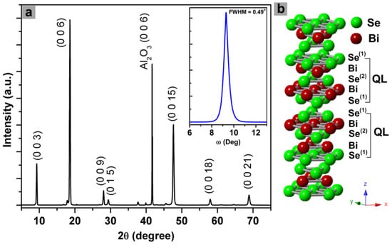
Figure 1.
(a) X-ray diffraction (XRD) patterns of a bismuth selenide (Bi2Se3) thin film grown on c-plane sapphire using pulsed laser deposition (PLD). The inset in (a) shows the XRD rocking curve of (006) peak for the film. (b) Crystal structure of Bi2Se3 (QL is quintuple layer).
Intriguingly, the films presented polycrystalline morphology with mutually crossed nanoplatelets (Figure 2a), which are somehow similar to those of Bi2Te3 grown by electrodeposition [40]. It has been proposed that the formation of mutually crossed Bi2Te3 nanoplatelets can be mainly attributed to the anisotropic bonding nature and growth facet planes with appropriate chemical stoichiometry [40]. This formation mechanism may be also prevailing in the present Bi2Se3 films due to the similar anisotropic bonding nature of Bi2Se3 and Bi2Te3. The film exhibited layered structure and uniform thickness of ~360 nm, as shown by the cross-sectional SEM image in Figure 2a. The upper inset of Figure 2a summarizes the EDS result of the film. Clearly, the film obtained stoichiometric composition of Bi2Se3 (i.e., 40.56 at.% Bi and 59.44 at.% Se). The surface roughness can be represented by center line average (Ra), as shown by the AFM image in Figure 2b. The Ra of the film was 8.54 nm.
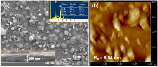
Figure 2.
(a) A plane-view SEM image of the Bi2Se3 thin film deposited on c-plane sapphire. Lower inset: a cross-sectional SEM image of the film; upper inset: The energy-dispersive X-ray spectroscopy (EDS) spectra and relative compositions of the film. (b) AFM image of the film, Ra is the center line average roughness.
Figure 3a displays the typical load-displacement curve of the present Bi2Se3 films obtained by CSM. The corresponding indentation depth-dependent hardness and Young’s modulus are shown in Figure 3b,c, respectively. As is evident from Figure 3b, the indentation depth-dependent hardness of Bi2Se3 thin film can be roughly divided into two stages. Namely, the hardness, after reaching the maximum in the first 10 nm, precipitously decreases with further increasing indentation depth and eventually reaches a constant value at 2.1 ± 0.1 GPa after the first stage. It is noted that the present results are well within the 30% depth/thickness criterion for nanoindentation test suggested by Li et al. [23,41]. Thus, the effects arising from the substrate or film/substrate interface are excluded. In this respect, the “noisy” depth-dependent hardness, especially in the first stage, might be arisen from the extensive dislocation activities in this stress range. Similar tendency in the depth-dependent Young’s modulus is observed (Figure 3c), presumably due to the same mechanism. The Young’s modulus of the present Bi2Se3 thin film is 58.6 ± 4.1 GPa. It is interesting to note that both the hardness and Young’s modulus of present PLD-derived Bi2Se3 thin films are much larger than that of single-crystal Bi2Se3 reported by Gupta et al. [12], where the respective values of 85.09 MPa and 6.361 GPa were obtained. The reason for the apparent discrepancy is not clear at present. Nevertheless, in addition the apparent differences in microstructure, such as grain boundaries (see Figure 2a), we also note that the load and penetration depths carried out in Reference [12] were both much larger than that employed in the present study. Recently, it has been found in a hybrid double perovskite (MA)2AgBiBr6 that Young’s modulus decreased considerably with increasing indentation depth [42], which partially explains for the larger Young’s modulus in this study than that of in Reference [12].
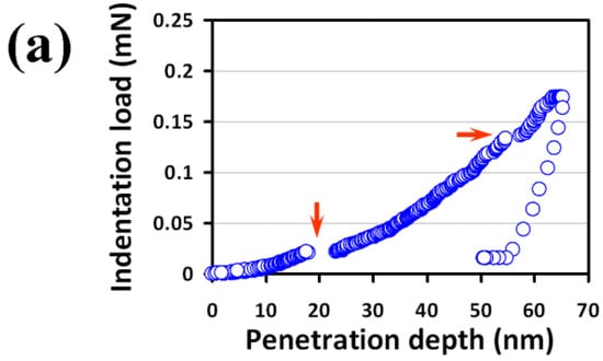
Figure 3.
(a) A load-displacement curve showing the multiple “pop-ins” during loading part, (b) hardness-displacement curve and, (c) Young’s modulus-displacement curve are obtained from the nanoindentation continuous contact stiffness (CSM) results of Bi2Se3 thin film.
From Figure 3a and the cyclic load-displacement curve in the inset of Figure 4, signatures of the multiple pop-ins are clearly observed in the loading part, as indicated by the arrows shown in both figures. It is noted that similar behaviors were also observed in nanoindented Bi2Se3 single crystals and was interpreted as being due to heterogeneous nucleation of dislocations beneath the indenter tip [12]. Since the multiple pop-ins is generally closely related to the sudden collective activities of dislocations [43] (such as dislocation generation or movement bursts), we believe that massive dislocation activities are the predominant deformation mechanism in this material, which, in fact, is also consistent with the conjectures of the resultant “noisy” features seen in the depth-dependent curves hardness and Young’s modulus described above.
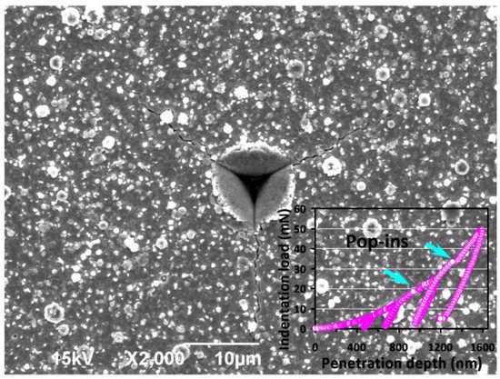
Figure 4.
Nanoindented SEM micrograph of Bi2Se3 thin film showing cracks propagate along the corners and pile-up beside the edges of the Berkovich indent. The inset shows the cyclic load-displacement curve at a load of 50 mN. Notice that the multiple “pop-ins” is observable (indicated by the arrows) in loading segments.
It is also interesting to note that no “pop-out” event is observed in both the unloading curves displayed in Figure 3a and in the inset of Figure 4. Such pop-out behavior is often interpreted as a manifestation of indentation-induced phase transition (for example: nanoindentation-induced phase transformation of single-crystal Si [44]), which is not found in our case. However, as revealed by the SEM image shown in Figure 4, it is evident that significant cracks and pile-ups phenomena along the three corners and edges of the residual indent are also observable. The multiple pop-ins were observed in a large array of materials and were demonstrated to result mainly from massive nucleation and/or propagation of dislocations during loading [45], or micro-cracks initiated around the indentation tip [46]. Hence, it is clear that not only the first pop-in event may reflect the onset of plasticity due to the dislocation activities, but the cracking and pile-up event could also be dominated by the similar mechanism in the present Bi2Se3 thin films under nanoindentation. On the other hand, the pressure-induced structural phase transition in Bi2Se3 using high pressure Raman and XRD experiments [47] has evidenced that the magnitude of required pressure to induce phase transitions is significantly higher than the apparent room-temperature hardness of hexagonal Bi2Se3 thin film measured here. It is worthwhile mentioning that in many hexagonal structured materials, such as, sapphire [48] and GaN thin films [49,50,51,52], the primary nanoindentation-induced deformation mechanisms have been consistently identified to be the nucleation and propagation of dislocations. It is, thus, plausible to state that deformation behavior in the present Bi2Se3 thin films is most likely governed by the similar mechanisms.
Within the scenario of the dislocation nucleation and propagation, the first pop-in event appearing in the loading segment naturally reflects the onset of plasticity for Bi2Se3 thin film, which also provides prominent information about the critical shear stress (τmax) the energy associated with the nucleation of dislocation loops. Following the analytical model proposed by Johnson [53], τmax can be related to the indentation load (Pc), at which a discontinuity in the load-displacement curve takes place, through the following equation [53]:
Here, R is the radius of indenter tip and Er is the effective elastic modulus, respectively. The maximum shear stress for Bi2Se3 thin films investigated in the present study is about 0.7 GPa. To the first approximation, the work done by this τmax is mainly associated with the dislocations nucleated within the deformation region underneath the indenter tip. Assuming the nucleation is homogeneous during nanoindentation [34], then, according to the classical dislocation theory [54], the stress at which the first “pop-in” taking place and the energy “dissipated” in it can be regarded, respectively, as the shear stress required to initiate plastic deformation and the energy required for generating a dislocation loop to prevail the deformation. The free energy (UF) of a circular dislocation loop with radius r can be written as:
where is the energy per unit length of the dislocation loop, b is the magnitude of Burgers vector (~0.4 nm) [55] and τ is the external shear stress acting on the dislocation loop, respectively. The first term on the right-hand side of Equation (2) describes the energy increased by forming a dislocation loop of radius r in an initially defect-free lattice. The second term is nothing but the strain energy released via work done by the applied stress (τ) to expand the dislocation loop over a displacement of one Burgers vector. The linear energy density () for a dislocation is given by [54]:
where G, vf and rcore are the shear modulus (≈24 GPa), the Poisson’s ratio (assumed to be 0.25) of Bi2Se3 thin film, and radius of dislocation core, respectively. Substituting Equation (1) and Equation (3) into Equation (2) gives:
Here, τc is the resolved shear stress of τmax on the active slip systems of the material and is usually taken as half value of τmax [56]. Equation (4) clearly indicates that UF contains terms with first and second power of r. Thus, there must exist a critical radius, rc, at which UF of the system reaches a maximum value. When the radius of the dislocation loop exceeds rc, further expansion lowers UF, hence is thermodynamically favorable. In contrast, if r < rc, the loop would shrink to reduce the energy. Consequently, when the loading reaches to the “pop-in” point, homogeneous formation of circular dislocation loop becomes possible without thermal energy at UF = 0 [57]. The condition (UF = 0) allows τc to be determined from through Equation (2) and Equation (3), yielding . Since τc has a maximum value as , one obtains: . The values of rcore and rc for the present Bi2Se3 thin films were calculated to be 1.08 nm and 5.4 nm, respectively.
By assuming that the nucleation of dislocation loops is entirely responsible for the indentation-induced plastic deformation and no thermal effect is involved, one can further estimate the number of dislocation loops formed during the first “pop-in” event by using the associated work-done (Wp). As depicted in Figure 5, the estimated Wp is ~0.11 × 10⁻¹² Nm, suggesting that ~8 × 10³ dislocation loops with critical diameter might have been formed. Although the estimated number is relatively low compared to that of typical polycrystalline thin films (~106 cm−2) [58], it is, nevertheless, consistent with the scenario that the “pop-in” is induced by massive homogeneous dislocation nucleation, instead of by the activated collective motion of pre-existing grown-in dislocations [34]. Alternatively, one can take the total dissipation energy as the energy to estimate the number of dislocations with critical radius being generated during entire nanoindentation practice. In that case, as high as ~3 × 10⁵ dislocation loops may be formed during nanoindentation. This number, albeit not entirely realistic, may be considered as the upper limit within the context of dislocation dominant deformation mechanism.
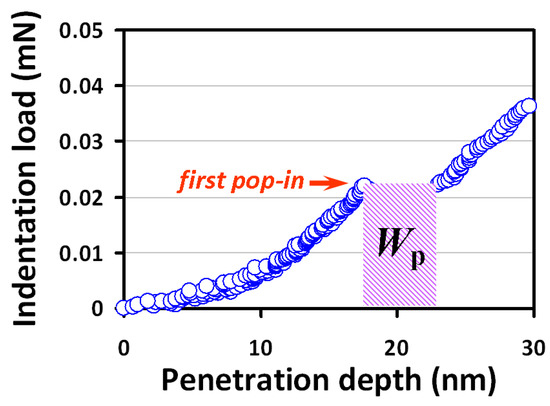
Figure 5.
The corresponding first pop-in event from Figure 3a is zoomed in to depict the plastic strain work, Wp, which is approximated as the product of critical loading and the sudden incremental displacement indicated by the shaded area.
4. Conclusions
To sum up, XRD, SEM, AFM and nanoindentation techniques are used to investigate the microstructural and surface morphological features, as well as the nanomechanical properties of Bi2Se3 thin films. The results show that the Bi2Se3 thin films are polycrystalline with highly (00l)-orientation (texture films) and stoichiometric compositions. The hardness and Young’s modulus of Bi2Se3 thin film are obtained 2.1 ± 0.1 GPa and 58.6 ± 4.1 GPa, respectively. Similar to many hexagonal-structured semiconductors, the primary deformation mechanism for the present Bi2Se3 thin film is governed by nucleation and propagation of dislocations or the formation of cracking events. Preliminary energetic estimations indicated that the number of dislocation loops induced by nanoindentation to trigger the plastic deformation accounts for the first pop-in event was in the order of 103 with a critical radius (rc ≈ 5.4 nm). Although the estimated dislocation density is relatively low compared to that of typical polycrystalline films, it is, nevertheless, in line with the scenario of homogeneous dislocation nucleation-induced first “pop-in” event.
Author Contributions
H.-D.L. contributed to the nanoindentation experiments and analyses. L.T.C.T. and P.H.L. carried out the growth of Bi2Se3 thin films and performed XRD and SEM-EDS data. C.-W.L., J.-Y.J. and S.-R.J. contributed to the discussion on materials characterizations. S.-R.J. designed the project of experiments and drafted the manuscript. All authors read and approved the final manuscript.
Acknowledgments
Financial supports from the Ministry of Science and Technology, Taiwan under Contract Nos.: MOST 106-2112-M009-013-MY3, MOST 103-2112-M-009-015-MY3, MOST 107-2112-M-214-001, MOST 106-2112-M-214-001, MOST 105-2112-M-214-001, and Vietnam National Foundation for Science and Technology Development (NAFOSTED) under grant number 103.99–2015.17 are gratefully acknowledged.
Conflicts of Interest
The authors declare no conflicts of interest.
References
- Zhang, H.; Liu, C.-X.; Qi, X.-L.; Dai, X.; Fang, Z.; Zhang, S.-C. Topological insulators in Bi2Se3, Bi2Te3 and Sb2Te3 with a single Dirac cone on the surface. Nat. Phys. 2009, 5, 438–442. [Google Scholar] [CrossRef]
- Moore, J.E. The birth of topological insulators. Nature 2010, 464, 194–198. [Google Scholar] [CrossRef] [PubMed]
- Yazyev, O.V.; Moore, J.E.; Louie, S.G. Spin Polarization and Transport of Surface States in the Topological Insulators Bi2Se3 and Bi2Te3 from First Principles. Phys. Rev. Lett. 2010, 105, 266806. [Google Scholar] [CrossRef] [PubMed]
- Min, W.-L.; Betancourt, A.P.; Jiang, P.; Jiang, B. Bioinspired broadband antireflection coatings on GaSb. Appl. Phys. Lett. 2008, 92, 141109. [Google Scholar] [CrossRef]
- Qi, X.-L.; Zhang, S.-C. Topological insulators and superconductors. Rev. Mod. Phys. 2011, 83, 1057–1110. [Google Scholar] [CrossRef]
- Hsieh, D.; Qian, D.; Wray, L.; Xia, Y.; Hor, Y.S.; Cava, R.J.; Hasan, M.Z. A topological Dirac insulator in a quantum spin Hall phase. Nature 2008, 452, 970–974. [Google Scholar] [CrossRef] [PubMed]
- Xia, Y.; Qian, D.; Hsieh, D.; Wray, L.; Pal, A.; Lin, H.; Bansil, A.; Grauer, D.; Hor, Y.S.; Cava, R.J.; et al. Observation of a large-gap topological-insulator class with a single Dirac cone on the surface. Nat. Phys. 2009, 5, 398–402. [Google Scholar] [CrossRef]
- Wiedmann, S.; Jost, A.; Fauqué, B.; van Dijk, J.; Meijer, M.J.; Khouri, T.; Pezzini, S.; Grauer, S.; Schreyeck, S.; Brüne, C.; et al. Anisotropic and strong negative magnetoresistance in the three-dimensional topological insulator Bi2Se3. Phys. Rev. B 2016, 94, 081302(R). [Google Scholar] [CrossRef]
- Le, P.H.; Liao, C.-N.; Luo, C.W.; Lin, J.-Y.; Leu, J. Thermoelectric properties of bismuth-selenide films with controlled morphology and texture grown using pulsed laser deposition. Appl. Surf. Sci. 2013, 285, 657–663. [Google Scholar] [CrossRef]
- Hor, Y.S.; Richardella, A.; Roushan, P.; Xia, Y.; Checkelsky, J.G.; Yazdani, A.; Hasan, M.Z.; Ong, N.P.; Cava, R.J. P-type Bi2Se3 for topological insulator and low-temperature thermoelectric applications. Phys. Rev. B 2009, 79, 195208. [Google Scholar] [CrossRef]
- Wang, E.; Ding, H.; Fedorov, A.V.; Yao, W.; Li, Z.; Lv, Y.-F.; Zhao, K.; Zhang, L.-G.; Xu, Z.; Schneeloch, J.; et al. Fully gapped topological surface states in Bi2Se3 films induced by a d-wave high-temperature superconductor. Nat. Phys. 2013, 9, 621–625. [Google Scholar] [CrossRef]
- Gupta, S.; Vijayan, N.; Krishna, A.; Thukral, K.; Maurya, K.K.; Muthiah, S.; Dhar, A.; Singh, B.; Bhagavannarayana, G. Enhancement of thermoelectric figure of merit in Bi2Se3 crystals through a necking process. J. Appl. Crystallogr. 2015, 48, 533–541. [Google Scholar] [CrossRef]
- Chen, J.; Qin, H.J.; Yang, F.; Liu, J.; Guan, T.; Qu, F.M.; Zhang, G.H.; Shi, J.R.; Xie, X.C.; Yang, C.L.; et al. Gate-voltage control of chemical potential and weak anti-localization in bismuth selenide. Phys. Rev. Lett. 2010, 105, 176602. [Google Scholar] [CrossRef] [PubMed]
- Liu, Y.; Weinert, M.; Li, L. Spiral growth without dislocations: Molecular beam epitaxy of the topological insulator Bi2Se3 on epitaxial graphene/SiC(0001). Phys. Rev. Lett. 2012, 108, 115501. [Google Scholar] [CrossRef] [PubMed]
- Tarakina, N.V.; Schreyeck, S.; Borzenko, T.; Schumacher, C.; Karczewski, G.; Brunner, K.; Gould, C.; Buhmann, H.; Molenkamp, L.W. Comparative study of the microstructure of Bi2Se3 thin films grown on Si(111) and InP(111) substrates. Cryst. Growth Des. 2012, 12, 1913–1918. [Google Scholar] [CrossRef]
- Wang, Z.Y.; Li, H.D.; Guo, X.; Ho, W.K.; Xie, M.H. Growth characteristics of topological insulator Bi2Se3 films on different substrates. J. Cryst. Growth 2011, 334, 96–102. [Google Scholar] [CrossRef]
- Onose, Y.; Yoshimi, R.; Tsukazaki, A.; Yuan, H.; Hidaka, T.; Iwasa, Y.; Kawasaki, M.; Tokura, Y. Pulsed Laser Deposition and Ionic Liquid Gate Control of Epitaxial Bi2Se3 Thin Films. Appl. Phys. Express 2011, 4, 83001. [Google Scholar] [CrossRef]
- Le, P.H.; Wu, K.H.; Luo, C.W.; Leu, J. Growth and characterization of topological insulator Bi2Se3 thin films on SrTiO3 using pulsed laser deposition. Thin Solid Films 2013, 534, 659–665. [Google Scholar] [CrossRef]
- Lee, Y.F.; Punugupati, S.; Wu, F.; Jin, Z.; Narayan, J.; Schwartz, J. Evidence for topological surface states in epitaxial Bi2Se3 thin film grown by pulsed laser deposition through magneto-transport measurements. Curr. Opin. Solid State Mater. Sci. 2014, 18, 279–285. [Google Scholar] [CrossRef]
- Orgiani, P.; Bigi, C.; Kumar Das, P.; Fujii, J.; Ciancio, R.; Gobaut, B.; Galdi, A.; Sacco, C.; Maritato, L.; Torelli, P.; et al. Structural and electronic properties of Bi2Se3 topological insulator thin films grown by pulsed laser deposition. Appl. Phys. Lett. 2017, 110, 171601. [Google Scholar] [CrossRef]
- Al Bayaz, A.; Giani, A.; Foucaran, A.; Pascal-Delannoy, F.; Boyer, A. Electrical and thermoelectrical properties of Bi2Se3 grown by metal organic chemical vapour deposition technique. Thin Solid Films 2003, 441, 1–5. [Google Scholar] [CrossRef]
- Zhang, M. Properties of topological insulator Bi2Se3 films prepared by thermal evaporation growth on different substrates. Appl. Phys. A 2017, 123, 122. [Google Scholar] [CrossRef]
- Li, X.; Gao, H.; Murphy, C.J.; Caswell, K.K. Nanoindentation of Silver Nanowires. Nano Lett. 2003, 3, 1495–1498. [Google Scholar] [CrossRef]
- Bao, L.; Xu, Z.-H.; Li, R.; Li, X.D. Catalyst-free synthesis and structural and mechanical characterization of single crystalline Ca2B2O5.H2O nanobelts and stacking faulted Ca2B2O5 nanogrooves. Nano Lett. 2010, 10, 255–262. [Google Scholar] [CrossRef] [PubMed]
- Nagar, R.; Teki, R.; Koratkar, N.; Sathe, V.G.; Kanjilal, D.; Mehta, B.R.; Singh, J.P. Radiation induced modification in nanoscale hardness of ZnO cone structures. J. Appl. Phys. 2010, 108. [Google Scholar] [CrossRef]
- Jian, S.-R.; Sung, T.-H.; Huang, J.C.; Juang, J.-Y. Deformation behaviors of InP pillars under uniaxial compression. Appl. Phys. Lett. 2012, 101, 151905. [Google Scholar] [CrossRef]
- Chen, G.-J.; Jian, S.-R. Effects of Cu doping on the structural and nanomechanical properties of ZnO thin films. Appl. Phys. A 2018, 124, 575. [Google Scholar] [CrossRef]
- Jian, S.-R.; Chen, G.-J.; Lee, J.-W. Effects of annealing temperature on nanomechanical and microstructural properties of Cu-doped In2O3 thin films. Appl. Phys. A 2017, 123, 726. [Google Scholar] [CrossRef]
- Jian, S.-R.; Le, P.H.; Luo, C.-W.; Juang, J.-Y. Nanomechanical and wettability properties of Bi2Te3 thin films: Effects of post-annealing. J. Appl. Phys. 2017, 121, 175302. [Google Scholar] [CrossRef]
- Le, P.H.; Chiu, S.-P.; Jian, S.-R.; Luo, C.W.; Lin, J.-Y.; Lin, J.-J.; Wu, K.H.; Gospodinov, M. Nanomechanical, structural, and transport properties of Bi3Se2Te thin films. J. Alloys Compd. 2016, 679, 350–357. [Google Scholar] [CrossRef]
- Chiu, Y.J.; Shen, C.-Y.; Chang, H.-W.; Jian, S.-R. Characteristics of Iron-Palladium alloy thin films deposited by magnetron sputtering. Results Phys. 2018, 9, 17–22. [Google Scholar] [CrossRef]
- Nawaz, A.; Mao, W.G.; Lu, C.; Shen, Y.G. Mechanical properties, stress distributions and nanoscale deformation mechanisms in single crystal 6H-SiC by nanoindentation. J. Alloys Compd. 2017, 708, 1046–1053. [Google Scholar] [CrossRef]
- Yen, C.-Y.; Jian, S.-R.; Tseng, Y.-C.; Juang, J.-Y. The deformation behavior and fracture toughness of single crystal YSZ(111) by indentation. J. Alloys Compd. 2018, 735, 2423–2427. [Google Scholar] [CrossRef]
- Lorenz, D.; Zeckzer, A.; Hilpert, U.; Grau, P.; Johansen, H.; Leipner, H.S. Pop-in effect as homogeneous nucleation of dislocations during nanoindentation. Phys. Rev. B 2003, 67, 172101. [Google Scholar] [CrossRef]
- Zhu, C.; Lu, Z.P.; Nieh, T.G. Incipient plasticity and dislocation nucleation of FeCoCrNiMn high-entropy alloy. Acta Mater. 2013, 61, 2993–3001. [Google Scholar] [CrossRef]
- Remington, T.P.; Ruestes, C.J.; Bringa, E.M.; Remington, B.A.; Lu, C.H.; Kad, B.; Meyers, M.A. Plastic deformation in nanoindentation of tantalum: A new mechanism for prismatic loop formation. Acta Mater. 2014, 78, 378–393. [Google Scholar] [CrossRef]
- Jian, S.-R.; Ke, W.C.; Juang, J.-Y. Mechanical characteristics of Mg-doped GaN thin films by nanoindentation. Nanosci. Nanotechnol. Lett. 2012, 4, 598–603. [Google Scholar] [CrossRef]
- Li, X.; Bhushan, B. A review of nanoindentation continuous stiffness measurement technique and its applications. Mater. Charact. 2002, 48, 11–36. [Google Scholar] [CrossRef]
- Oliver, W.C.; Pharr, G.M. An improved technique for determining hardness and elastic modulus using load and displacement sensing indentation experiments. J. Mater. Res. 1992, 7, 1564–1583. [Google Scholar] [CrossRef]
- Liao, C.-N.; Shih, H.-D.; Su, P.-W. Electrocrystallization of Mutually Crossed Bismuth Telluride Nanoplatelets. J. Electrochem. Soc. 2010, 157, D605–D608. [Google Scholar] [CrossRef]
- Bhushan, B.; Li, X. Nanomechanical characterisation of solid surfaces and thin films. Int. Mater. Rev. 2003, 48, 125–164. [Google Scholar] [CrossRef]
- Wei, F.; Deng, Z.; Sun, S.; Zhang, F.; Evans, D.M.; Kieslich, G.; Tominaka, S.; Carpenter, M.A.; Zhang, J.; Bristowe, P.D.; Cheetham, A.K. Synthesis and properties of a lead-free hybrid double perovskite: (CH3NH3)2AgBiBr6. Chem. Mater. 2017, 29, 1089–1094. [Google Scholar] [CrossRef]
- Mosca, D.H.; Mattoso, N.; Lepienski, C.M.; Veiga, W.; Mazzaro, I.; Etgens, V.H.; Eddrief, M. Mechanical properties of layered InSe and GaSe single crystals. J. Appl. Phys. 2002, 91, 140–144. [Google Scholar] [CrossRef]
- Jian, S.-R.; Chen, G.-J.; Juang, J.-Y. Nanoindentation-induced phase transformation in (1 1 0)-oriented Si single-crystals. Curr. Opin. Solid State Mater. Sci. 2010, 14, 69–74. [Google Scholar] [CrossRef]
- Jian, S.-R.; Chen, G.-J.; Lin, T.-C. Berkovich nanoindentation on AlN thin films. Nanoscale Res. Lett. 2010, 5, 935–940. [Google Scholar] [CrossRef] [PubMed]
- Bull, S.J. Nanoindentation of coatings. J. Phys. D. Appl. Phys. 2005, 38, R393–R413. [Google Scholar] [CrossRef]
- Yu, Z.; Wang, L.; Hu, Q.; Zhao, J.; Yan, S.; Yang, K.; Sinogeikin, S.; Gu, G.; Mao, H.-K. Structural phase transitions in Bi2Se3 under high pressure. Sci. Rep. 2015, 5, 1–9. [Google Scholar] [CrossRef] [PubMed]
- Nowak, R.; Sekino, T.; Maruno, S.; Niihara, K. Deformation of sapphire induced by a spherical indentation on the (10ī0) plane. Appl. Phys. Lett. 1996, 68, 1063–1065. [Google Scholar] [CrossRef]
- Bradby, J.E.; Kucheyev, S.O.; Williams, J.S.; Wong-Leung, J.; Swain, M.V.; Munroe, P.; Li, G.; Phillips, M.R. Indentation-induced damage in GaN epilayers. Appl. Phys. Lett. 2002, 80, 383–385. [Google Scholar] [CrossRef]
- Jian, S.-R.; Juang, J.-Y. Nanoindentation-induced pop-in effects in GaN thin films. IEEE Trans. Nanotechnol. 2013, 12, 304–308. [Google Scholar] [CrossRef]
- Jian, S.-R. Cathodoluminescence rosettes in c-plane GaN films under Berkovich nanoindentation. Opt. Mater. 2013, 35, 2707–2709. [Google Scholar] [CrossRef]
- Jian, S.-R. Mechanical deformation induced in Si and GaN under Berkovich nanoindentation. Nanoscale Res. Lett. 2008, 3, 6–13. [Google Scholar] [CrossRef]
- Johnson, K.L. Contact Mechanics; Cambridge University Press: Cambridge, UK, 1985. [Google Scholar]
- Hirth, J.P.; Lothe, J. Theory of Dislocations; Wiley: Hoboken, NY, USA, 1981. [Google Scholar]
- Zhuang, A.; Li, J.-J.; Wang, Y.-C.; Wen, X.; Lin, Y.; Xiang, B.; Wang, X.; Zeng, J. Screw-dislocation-driven bidirectional spiral growth of Bi2Se3 nanoplates. Angew. Chemie Int. Ed. 2014, 53, 6425–6429. [Google Scholar] [CrossRef] [PubMed]
- Chiu, Y.L.; Ngan, A.H.W. Time-dependent characteristics of incipient plasticity in nanoindentation of a Ni3Al single crystal. Acta Mater. 2002, 50, 1599–1611. [Google Scholar] [CrossRef]
- Leipner, H.S.; Lorenz, D.; Zeckzer, A.; Lei, H.; Grau, P. Nanoindentation pop-in effect in semiconductors. Physica B 2001, 308–310, 446–449. [Google Scholar] [CrossRef]
- Imaizumi, M.; Ito, T.; Yamaguchi, M.; Kaneko, K. Effect of grain size and dislocation density on the performance of thin film polycrystalline silicon solar cells. J. Appl. Phys. 1997, 81, 7635–7640. [Google Scholar] [CrossRef]
© 2018 by the authors. Licensee MDPI, Basel, Switzerland. This article is an open access article distributed under the terms and conditions of the Creative Commons Attribution (CC BY) license (http://creativecommons.org/licenses/by/4.0/).