Modeling of Gate Stack Patterning for Advanced Technology Nodes: A Review


Abstract
:1. Introduction
2. Methods
2.1. Surface Representations
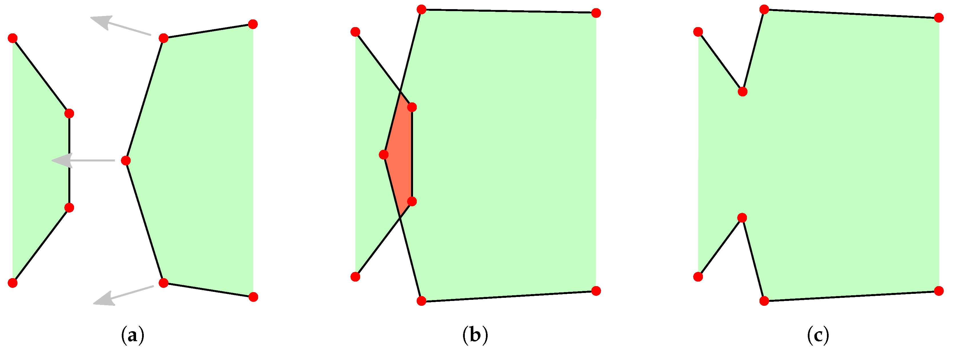
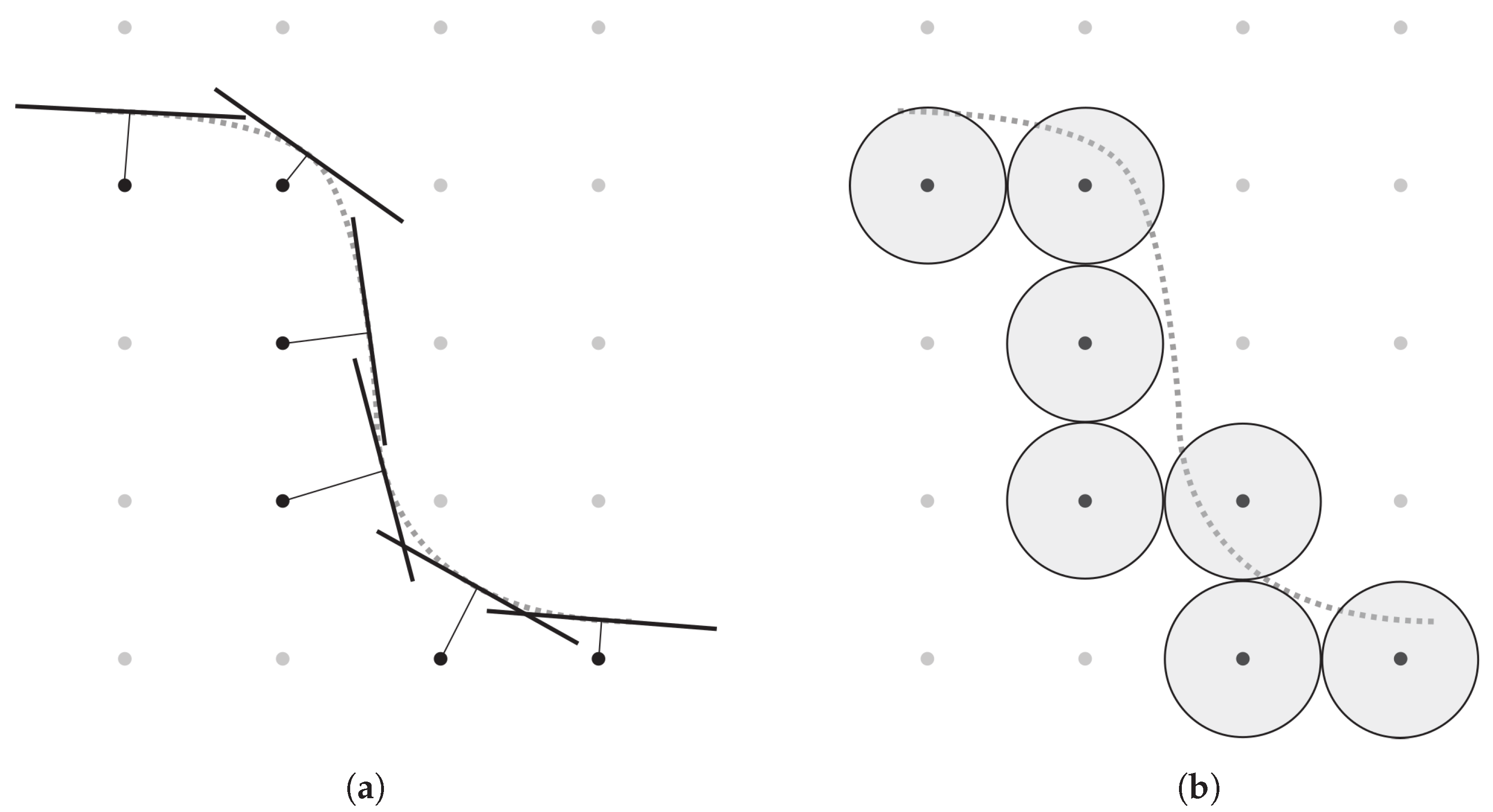
2.1.1. Explicit Surfaces
2.1.2. Implicit Surfaces
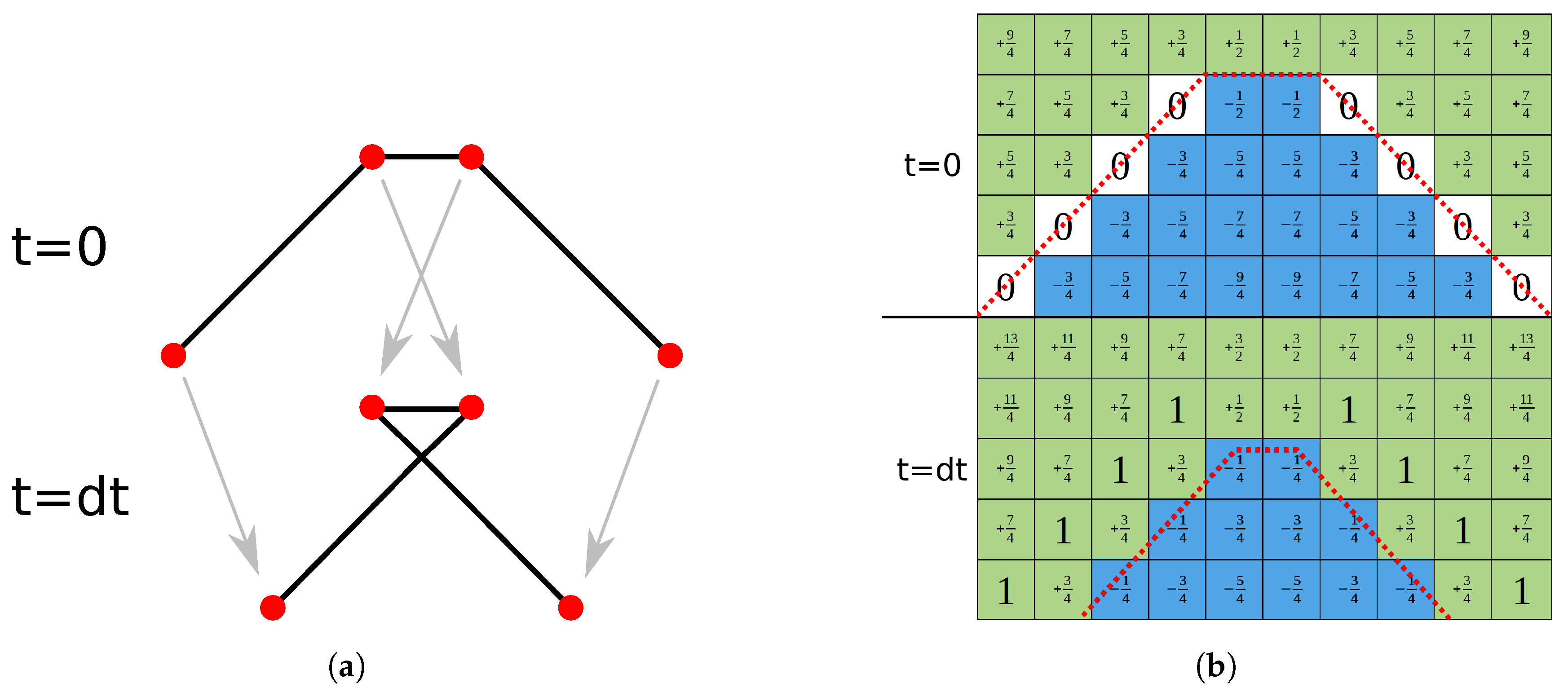
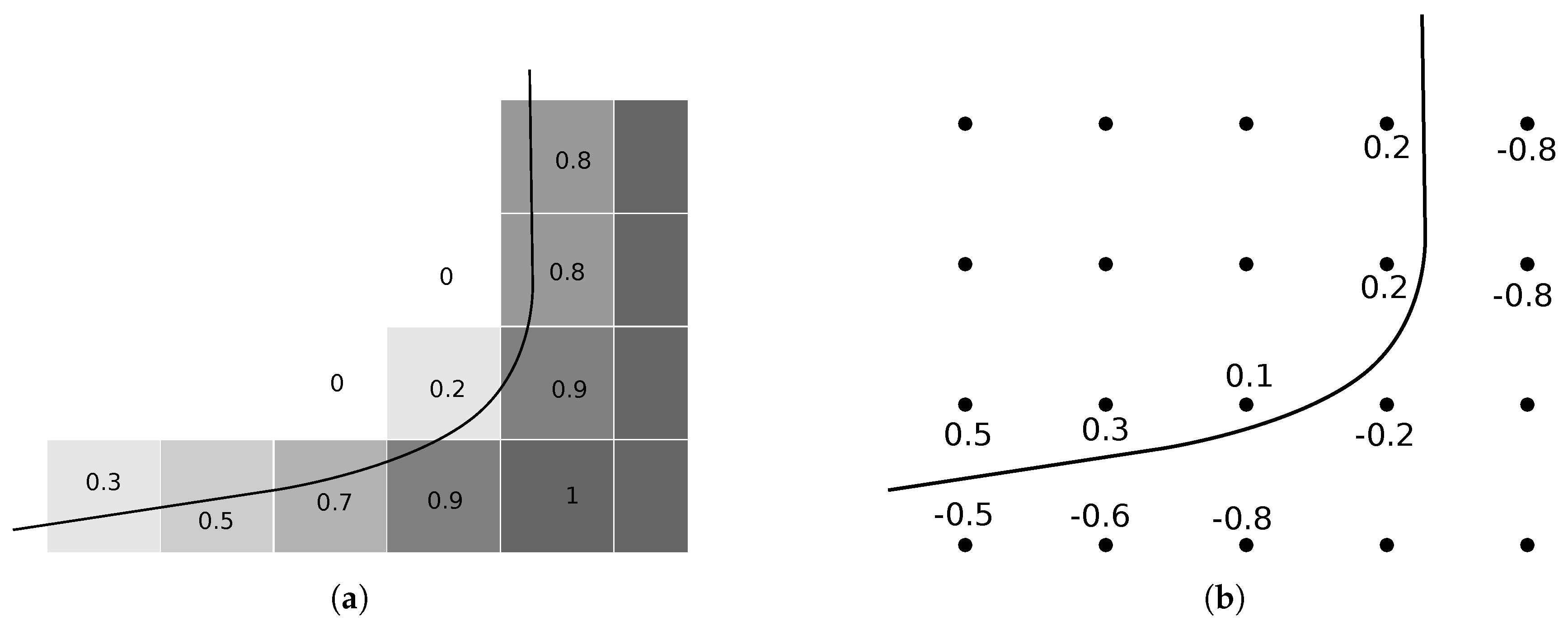
2.1.3. Cell Based Methods
2.2. Surface Velocity Calculation
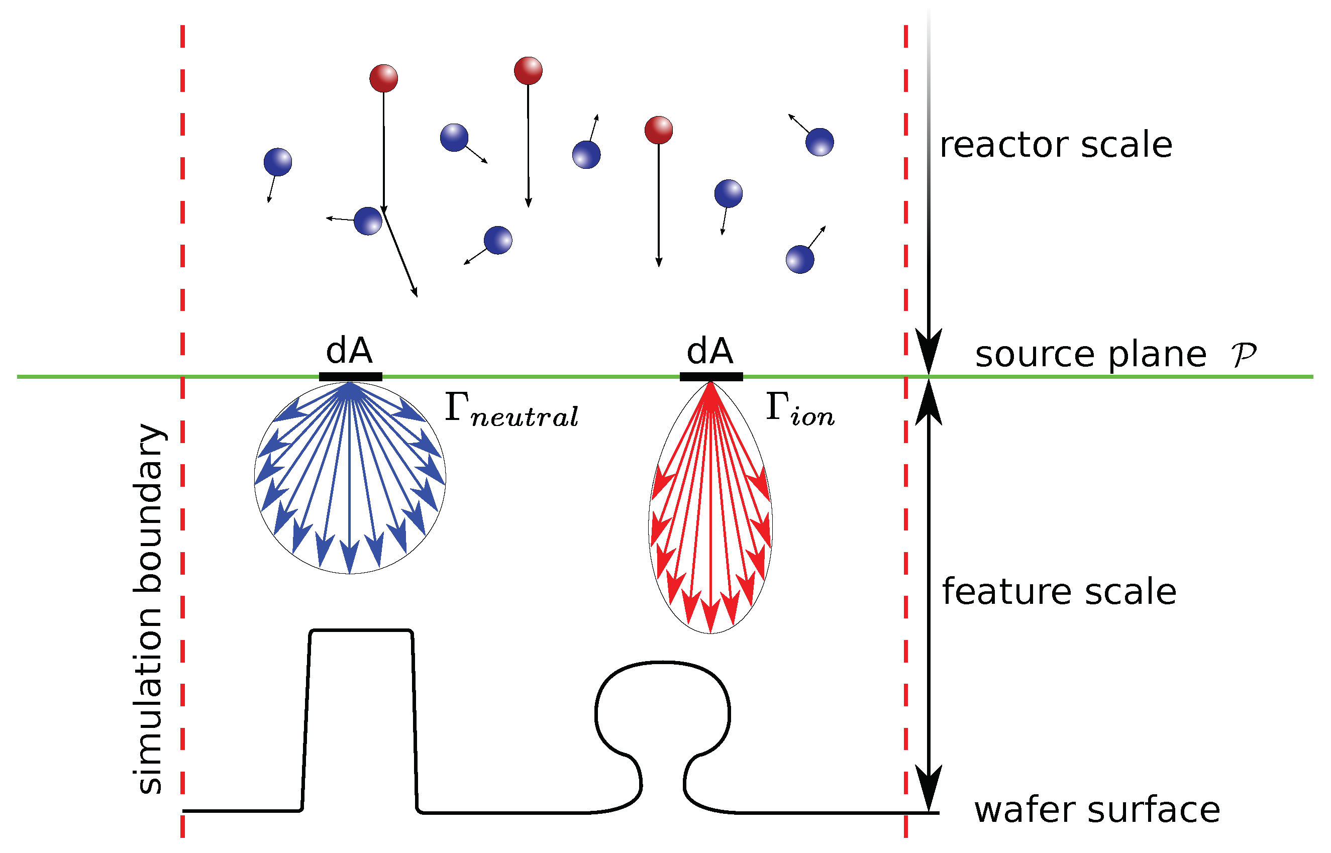
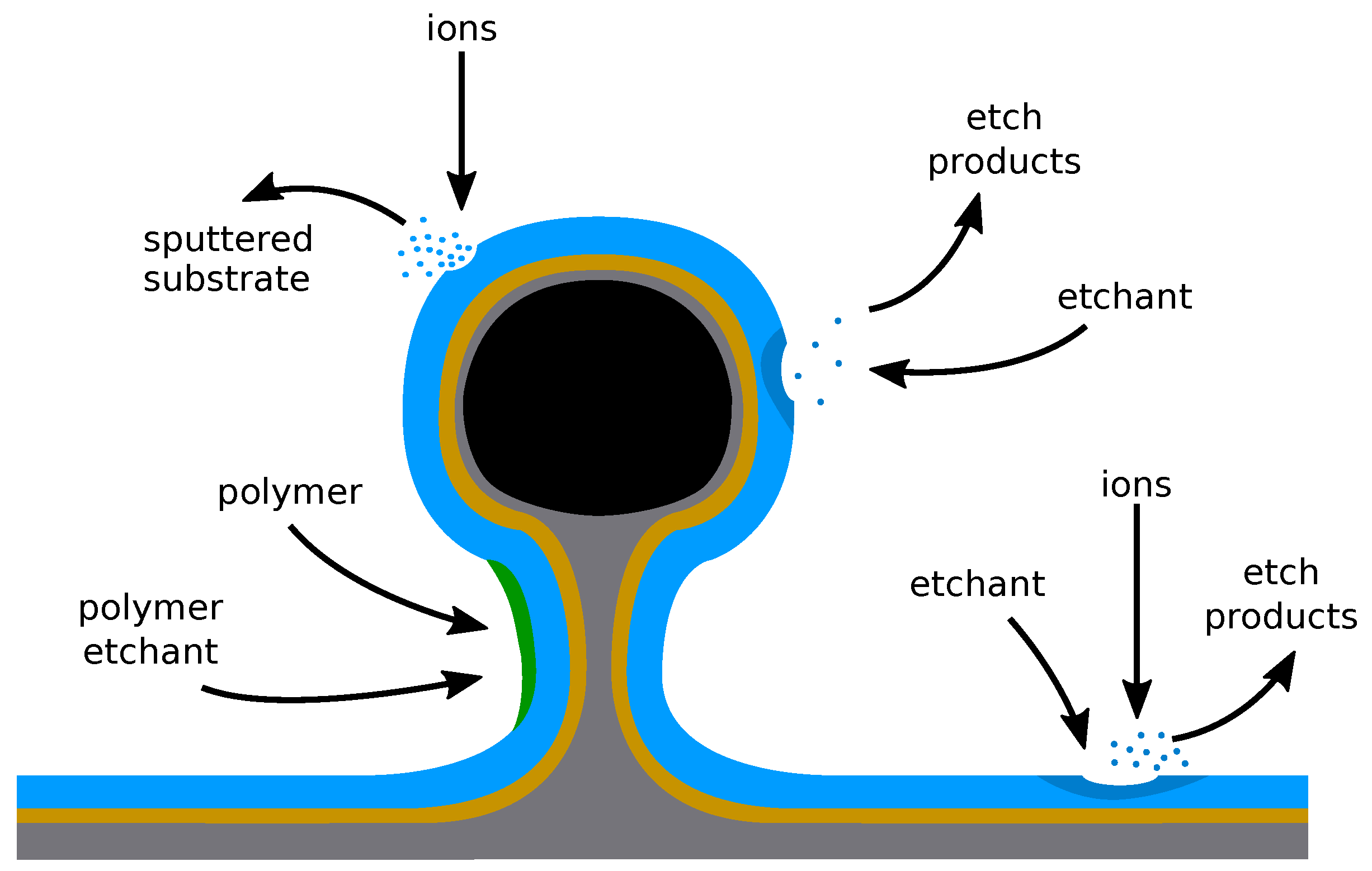
2.3. Transport of Molecular Entities in Plasma Environments
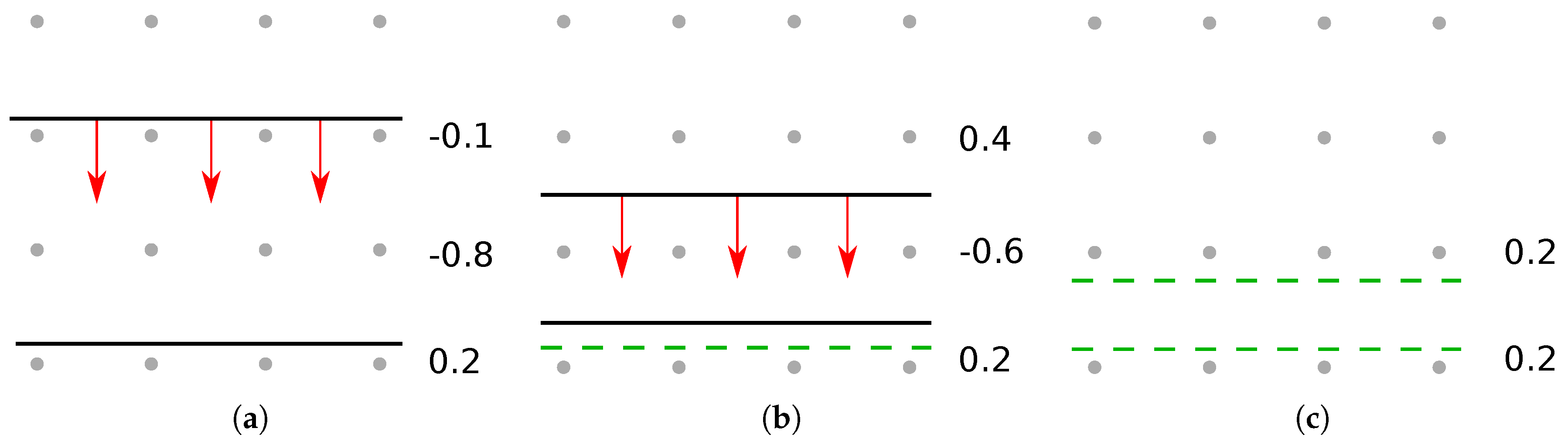
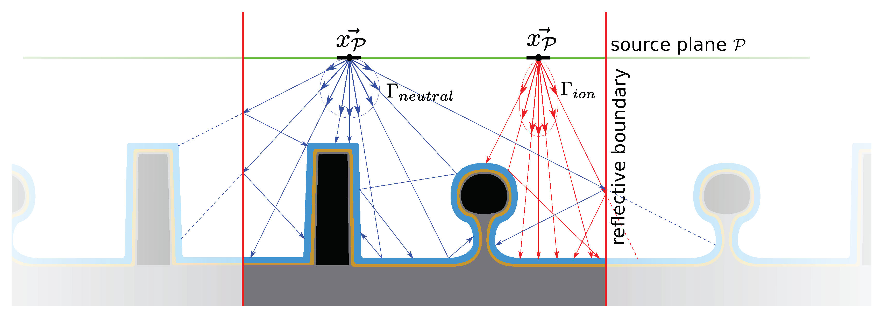
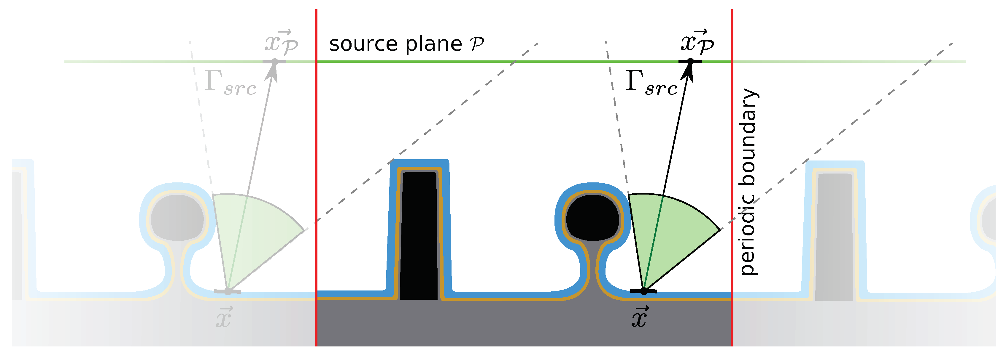
2.3.1. Top-Down Flux Calculation
2.3.2. Bottom-Up Flux Calculation
2.4. Chemical Modeling
3. Simulation Software
- Sentaurus Topography [78] is a commercial simulator developed by Synopsys (Mountain View, CA, USA), which uses level set based surface descriptions for topography changes, cell based representations for chemical surface reactions, and provides Monte Carlo methods for particle transport [79]. Dunn et al. [80] successfully used this tool to simulate the fabrication of FinFET structures of the 7 nm node. The Florida Object Oriented Process Simulator (FLOOPS) [81] provides similar capabilities. It was incorporated into Sentaurus, but a version is also available as an open-source project.
- Victory Process [82] is a proprietary process simulator distributed by Silvaco (Santa Clara, CA, USA). It allows level set surface descriptions, as well as explicit surfaces to be used. Nanda et al. [83] were able to simulate the fabrication of strained FinFETs using this framework. Victory Cell [84] is a related tool, which uses cell based and explicit surface representations in order to improve the description of ion implantation and diffusion. It was used by Maiti et al. [85] to simulate the fabrication of stressed FinFETs.
- ViennaTS [86] is an open-source feature scale process simulation tool developed at the Institute for Microelectronics, TU Wien. Surfaces are represented using level sets and top-down, as well as bottom-up methods, are implemented. The software provides predefined etch and deposition models, including several for the simulation of advanced node etching processes [77].
- The Monte Carlo Feature Profile Model (MCFPM) [87] is one of several software components developed at the Computational Plasma Science and Engineering Group, University of Michigan. Cell based methods are used to describe different materials and top-down approaches are used to describe particle transport. Combined with other software components, it was used by Huard et al. [88] to simulate the fabrication of advanced-node FinFETs.
4. Plasma Chemistries for Gate Stack Etching
4.1. Silicon Etching
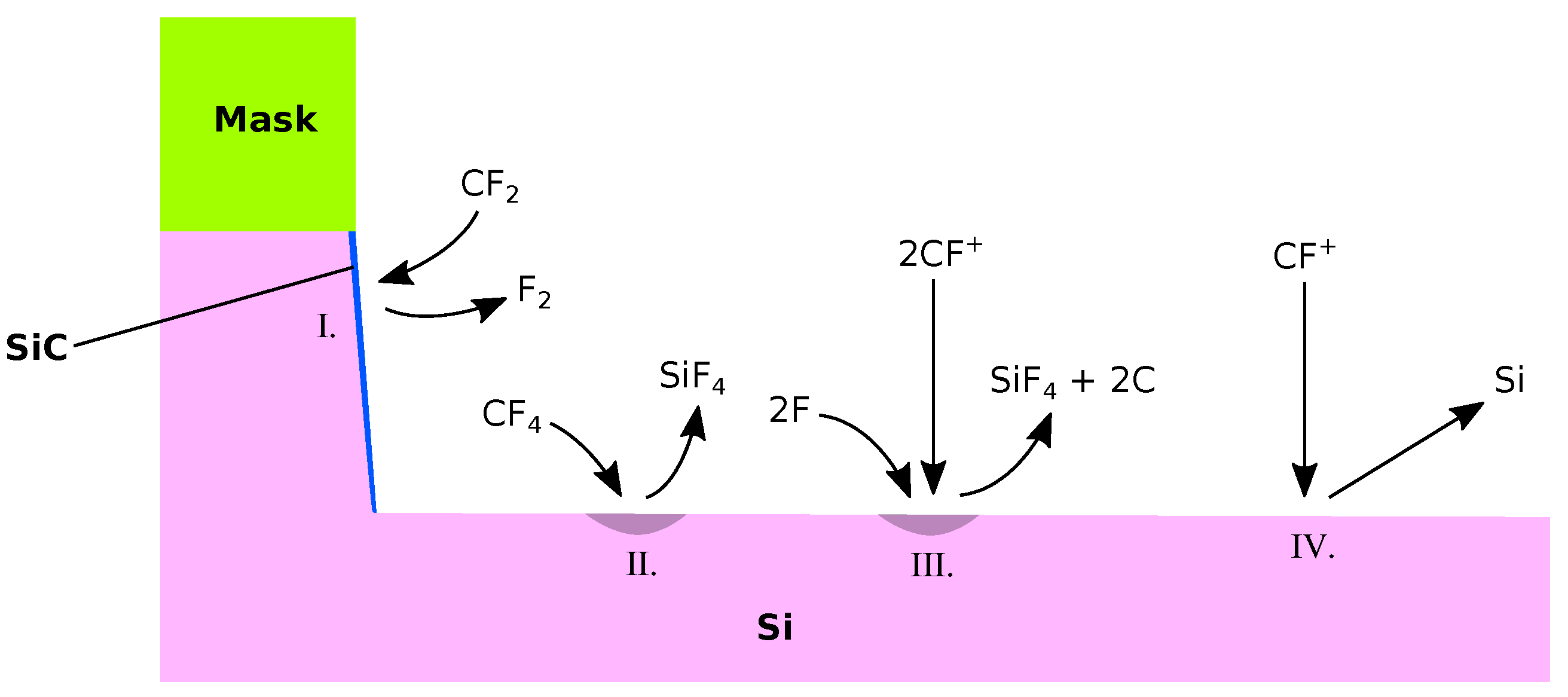
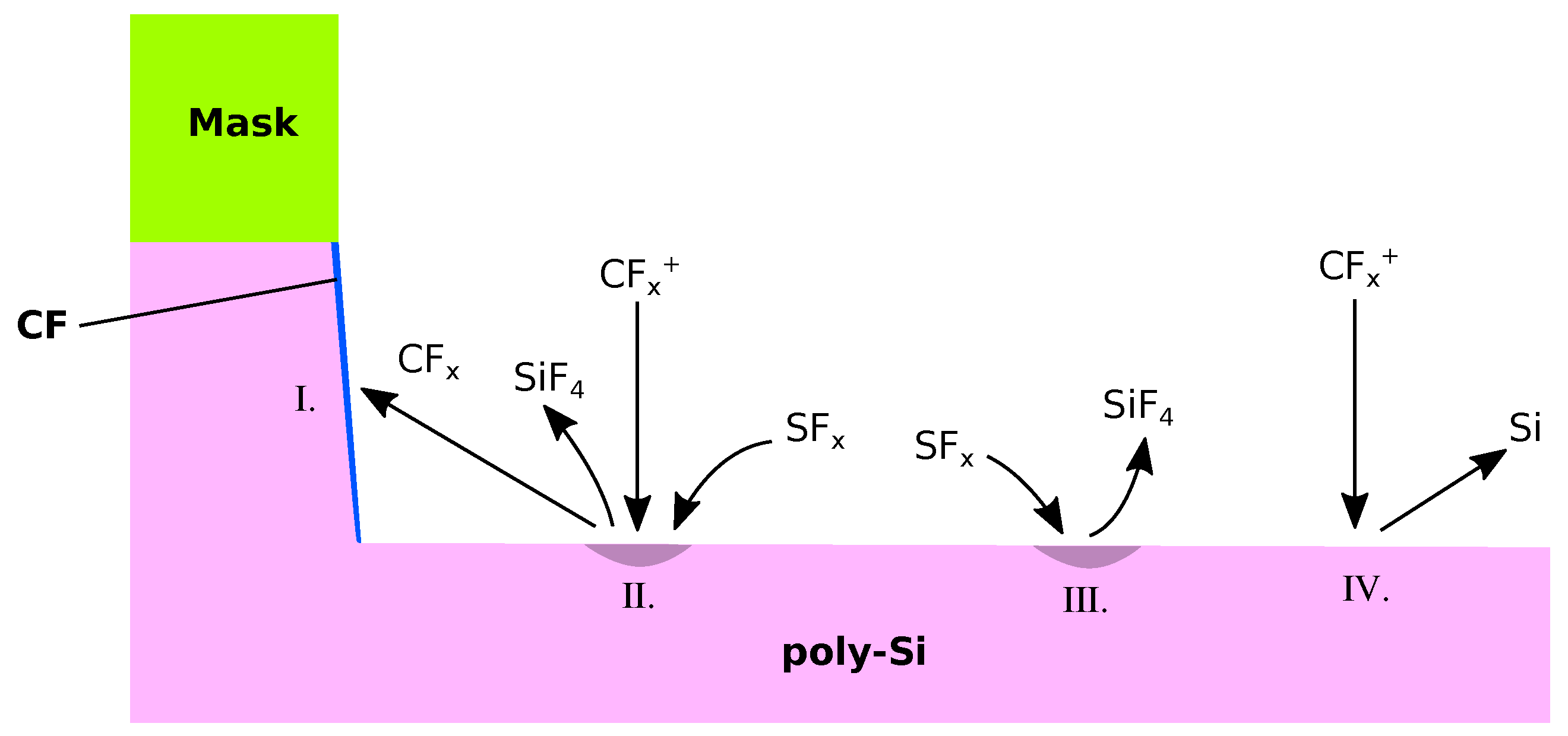
4.1.1. CF Type Chemistries
4.1.2. SF Type Chemistries
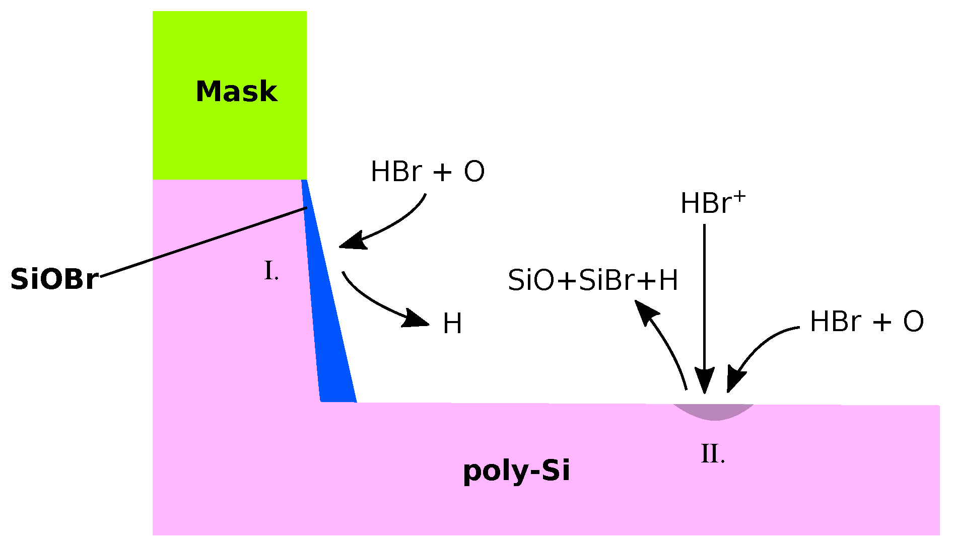
4.1.3. HBr Type Chemistries
4.2. TiN Etching
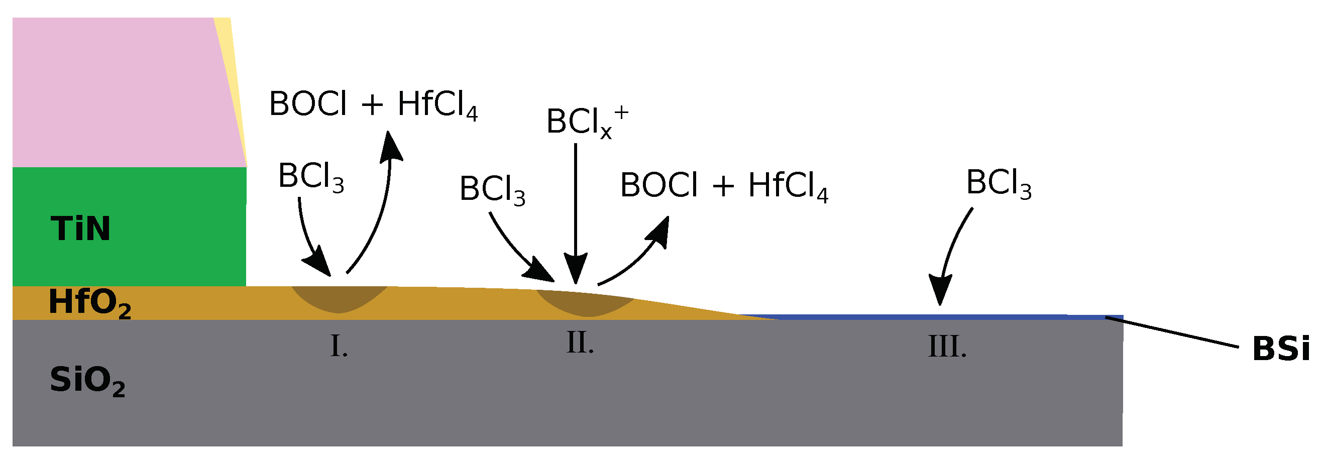
4.3. HfO2 Etching
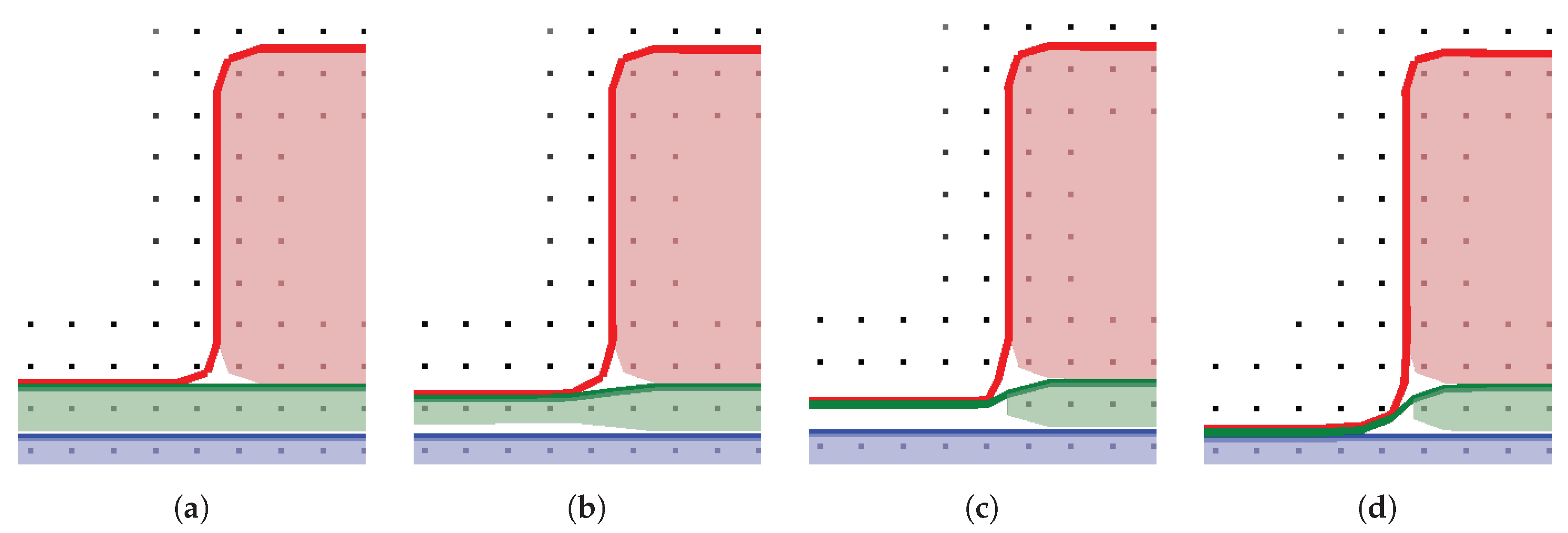
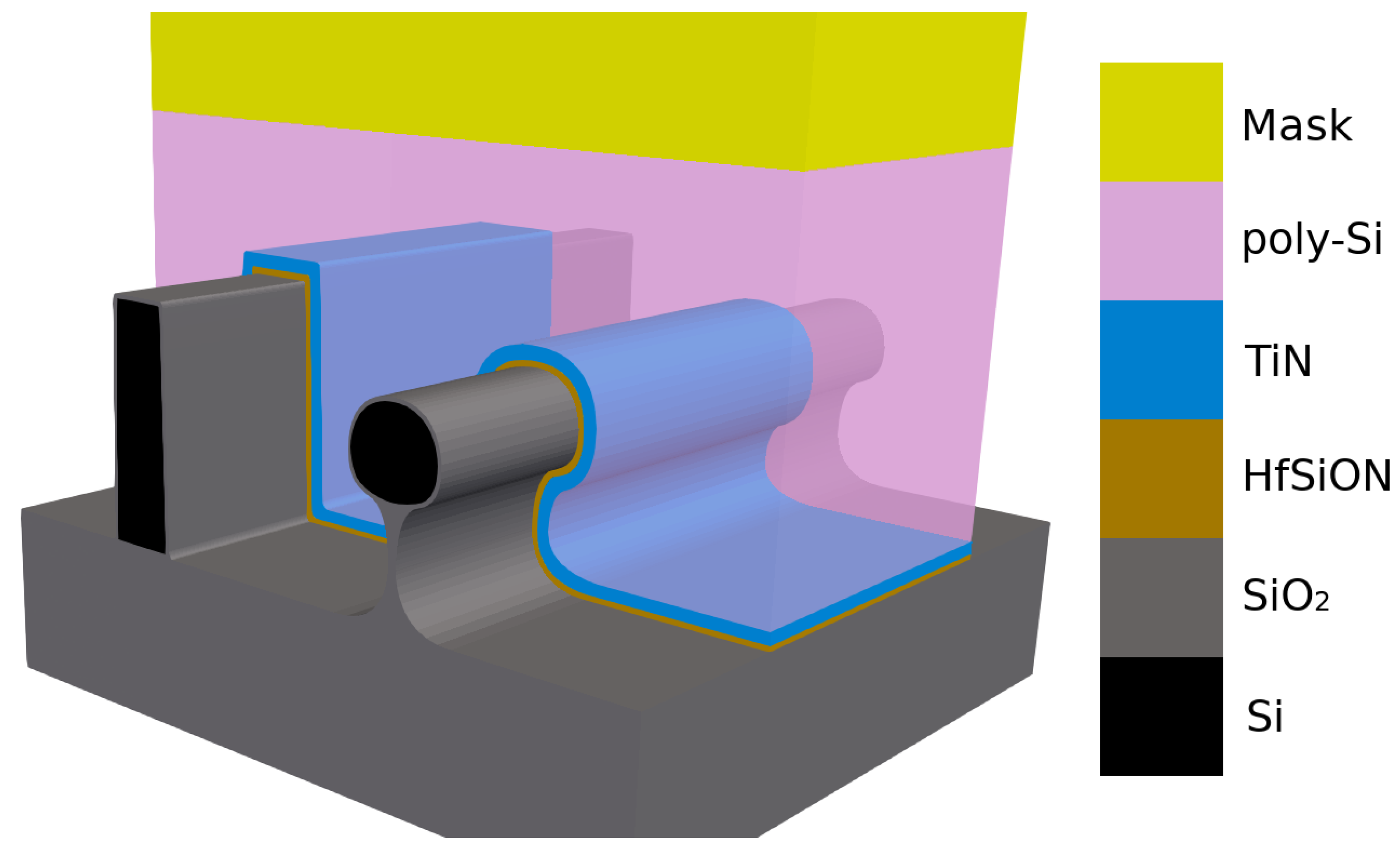
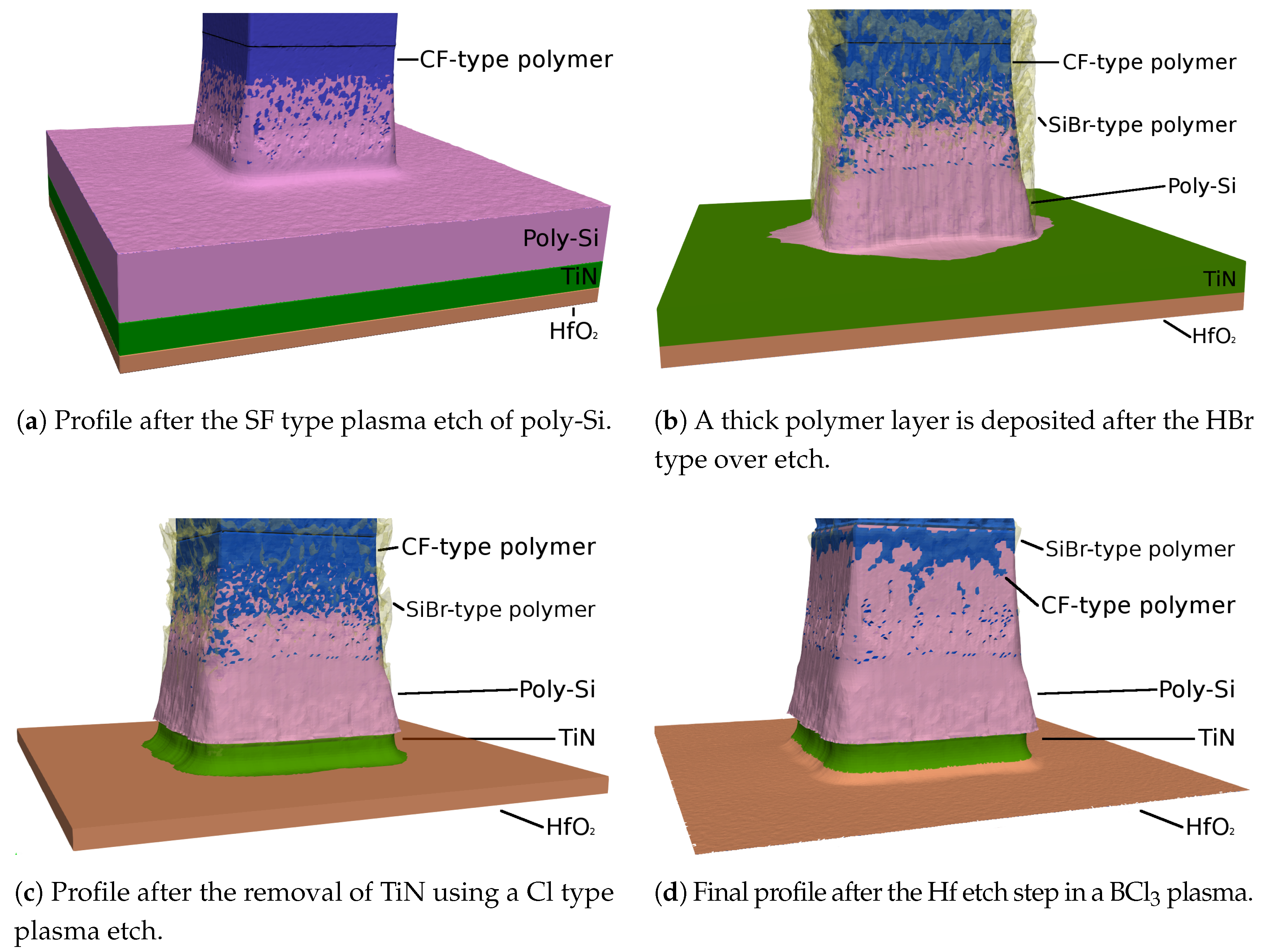
4.4. Full Etch Sequence
5. Conclusions
Author Contributions
Acknowledgments
Conflicts of Interest
References
- Moore, G.E. Progress in digital integrated electronics [Technical Digest—International Electron Devices Meeting, IEDM, 1975, Vol. 21, pp. 11–13.]. IEEE Solid-State Circuits Soc. Newsl. 2006, 11, 36–37. [Google Scholar] [CrossRef]
- Theis, T.N.; Wong, H.S.P. The end of Moore’s Law: A new beginning for information technology. Comput. Sci. Eng. 2016, 19, 41–50. [Google Scholar] [CrossRef]
- Lee, B.H.; Song, S.C.; Choi, R.; Kirsch, P. Metal electrode/high-k dielectric gate-stack technology for power management. IEEE Trans. Electron Devices 2008, 55, 8–20. [Google Scholar] [CrossRef]
- Robertson, J. Band offsets of wide-band-gap oxides and implications for future electronic devices. J. Vac. Sci. Technol. B Microelectron. Nanometer Struct. 2000, 18, 1785–1791. [Google Scholar] [CrossRef]
- Mistry, K.; Allen, C.; Auth, C.; Beattie, B.; Bergstrom, D.; Bost, M.; Brazier, M.; Buehler, M.; Cappellani, A.; Chau, R.; et al. A 45 nm logic technology with high-k+metal gate transistors, strained silicon, 9 Cu interconnect layers, 193 nm dry patterning, and 100% Pb-free packaging. In Proceedings of the 2007 IEEE International Electron Devices Meeting, Washington, DC, USA, 10–12 December 2007; pp. 247–250. [Google Scholar] [CrossRef]
- Lee, J.H.; Kim, D.G.; Lee, H.J.; Hwang, C.S. Fabrication of a nano-scaled tri-gate field effect transistor using the step-down patterning and dummy gate processes. Microelectron. Eng. 2017, 173, 33–41. [Google Scholar] [CrossRef]
- Pfiester, J.R.; Baker, F.K.; Mele, T.C.; Tseng, H.H.; Tobin, P.J.; Hayden, J.D.; Miller, J.W.; Gunderson, C.D.; Parrillo, L.C. The effects of boron penetration on p+ poly silicon gated PMOS devices. IEEE Trans. Electron Devices 1990, 37, 1842–1851. [Google Scholar] [CrossRef]
- Hobbs, C.C.; Fonseca, L.R.; Knizhnik, A.; Dhandapani, V.; Samavedam, S.B.; Taylor, W.J.; Grant, J.M.; Dip, L.R.G.; Triyoso, D.H.; Hegde, R.I.; et al. Fermi-level pinning at the polysilicon/metal oxide interface—Part I. IEEE Trans. Electron Devices 2004, 51, 971–977. [Google Scholar] [CrossRef]
- Lin, Y.S.; Huang, K.W.; Lin, H.C.; Chen, M.J. Effective work function modulation of the bilayer metal gate stacks by the Hf-doped thin TiN interlayer prepared by the in-situ atomic layer doping technique. Solid State Commun. 2017, 258, 49–53. [Google Scholar] [CrossRef]
- Huang, K.W.; Cheng, P.H.; Lin, Y.S.; Wang, C.I.; Lin, H.C.; Chen, M.J. Tuning of the work function of bilayer metal gate by in-situ atomic layer lamellar doping of AlN in TiN interlayer. J. Appl. Phys. 2017, 122, 095103. [Google Scholar] [CrossRef]
- Kim, C.K.; Ahn, H.J.; Moon, J.M.; Lee, S.; Moon, D.I.; Park, J.S.; Cho, B.J.; Choi, Y.K.; Lee, S.H. Temperature control for the gate workfunction engineering of TiC film by atomic layer deposition. Solid-State Electron. 2015, 114, 90–93. [Google Scholar] [CrossRef]
- Xiang, J.; Ding, Y.; Du, L.; Li, J.; Wang, W.; Zhao, C. Growth mechanism of atomic-layer-deposited TiAlC metal gate based on TiCl 4 and TMA precursors. Chin. Phys. B 2016, 25, 037308. [Google Scholar] [CrossRef]
- Hayes, M.H.; Dezelah, C.L.; Conley, J.F. Properties of Annealed Atomic-Layer-Deposited Ruthenium from Ru(DMBD)(CO)3 and Oxygen. ECS Trans. 2018, 85, 743–749. [Google Scholar] [CrossRef]
- The International Technology Roadmap for Semiconductors 2.0; The Optical Society: Washington, DC, USA, 2015.
- The International Roadmap for Devices and Systems; The Optical Society: Washington, DC, USA, 2017.
- Auth, C.; Allen, C.; Blattner, A.; Bergstrom, D.; Brazier, M.; Bost, M.; Buehler, M.; Chikarmane, V.; Ghani, T.; Glassman, T.; et al. A 22 nm high performance and low-power CMOS technology featuring fully-depleted tri-gate transistors, self-aligned contacts and high density MIM capacitors. In Proceedings of the 2012 Symposium on VLSI Technology (VLSIT), Honolulu, HI, USA, 12–14 June 2012; pp. 131–132. [Google Scholar] [CrossRef]
- Memos, G.; Lidorikis, E.; Kokkoris, G. The interplay between surface charging and microscale roughness during plasma etching of polymeric substrates. J. Appl. Phys. 2018, 123, 073303. [Google Scholar] [CrossRef]
- Bär, E.; Lorenz, J. 3-D simulation of LPCVD using segment-based topography discretization. IEEE Trans. Semicond. Manuf. 1996, 9, 67–73. [Google Scholar] [CrossRef]
- Thurgate, T. Segment-based etch algorithm and modeling. IEEE Trans. Comput.-Aided Des. Integr. Circuits Syst. 1991, 10, 1101–1109. [Google Scholar] [CrossRef]
- Pauly, M.; Gross, M.; Kobbelt, L.P. Efficient simplification of point-sampled surfaces. In Proceedings of the IEEE Visualization VIS 2002, Boston, MA, USA, 27 October–1 Novmber 2002; pp. 163–170. [Google Scholar] [CrossRef] [Green Version]
- Law, M. Grid adaption near moving boundaries in two dimensions for IC process simulation. IEEE Trans. Comput.-Aided Des. Integr. Circuits Syst. 1995, 14, 1223–1230. [Google Scholar] [CrossRef]
- Law, M.E.; Cea, S.M. Continuum based modeling of silicon integrated circuit processing: An object oriented approach. Comput. Mater. Sci. 1998, 12, 289–308. [Google Scholar] [CrossRef] [Green Version]
- Bloomenthal, J.; Wyvill, B.; Bajaj, C. Introduction to Implicit Surfaces; Morgan Kaufmann Publishers: San Francisco, CA, USA, 1997. [Google Scholar]
- Alliez, P.; de Verdire, E.; Devillers, O.; Isenburg, M. Isotropic surface remeshing. In Proceedings of the 2003 Shape Modeling International, Seoul, Korea, 12–15 May 2003; IEEE Computer Society: Washington, DC, USA, 2003; Volume 2003, pp. 49–58. [Google Scholar] [CrossRef]
- Sethian, J. Level Set Methods and Fast Marching Methods: Evolving Interfaces in Computational Geometry, Fluid Mechanics, Computer Vision, And Materials Science; Cambridge University Press: Cambridge, UK, 1999. [Google Scholar]
- Chacon, A.; Vladimirsky, A. Fast two-scale methods for eikonal equations. SIAM J. Sci. Comput. 2012, 34, A547–A578. [Google Scholar] [CrossRef]
- Adalsteinsson, D.; Sethian, J.A. The fast construction of extension velocities in level set methods. J. Comput. Phys. 1999, 148, 2–22. [Google Scholar] [CrossRef]
- Mauch, S. A Fast Algorithm for Computing the Closest Point and Distance Transform; Unpublished Technical Report; California Institute of Technology: Pasadena, CA, USA, 2000; pp. 1–17. [Google Scholar]
- Zhao, H.K. Fast sweeping method for eikonal equations. Math. Comput. 2005, 74, 603–627. [Google Scholar] [CrossRef]
- Sethian, J.A. A fast marching level set method for monotonically advancing fronts. Proc. Natl. Acad. Sci. USA 1996, 93, 1591–1595. [Google Scholar] [CrossRef] [PubMed]
- Osher, S.; Sethian, J.A. Fronts propagating with curvature-dependent speed: Algorithms based on hamilton-jacobi formulations. J. Comput. Phys. 1988, 79, 12–49. [Google Scholar] [CrossRef]
- Osher, S.; Shu, C.W. High-order essentially nonoscillatory schemes for Hamilton–Jacobi equations. SIAM J. Numer. Anal. 1991, 28, 907–922. [Google Scholar] [CrossRef]
- Whitaker, R.T. A level-set approach to 3D reconstruction from range data. Int. J. Comput. Vis. 1998, 29, 203–231. [Google Scholar] [CrossRef]
- Hsiau, Z.K.; Kan, E.C.; McVittie, J.P.; Dutton, R.W. Robust, stable, and accurate boundary movement for physical etching and deposition simulation. IEEE Trans. Electron Devices 1997, 44, 1375–1385. [Google Scholar] [CrossRef]
- Manstetten, P.L. Efficient Flux Calculations for Topography Simulation. Doctoral Thesis, Institute for Microelectronics, TU Wien, Austria, 2018. [Google Scholar]
- Pasko, A.; Adzhiev, V.; Sourin, A.; Savchenko, V. Function representation in geometric modeling: Concepts, implementation and applications. Vis. Comput. 1995, 11, 429–446. [Google Scholar] [CrossRef]
- Adalsteinsson, D.; Sethian, J.A. A fast level set method for propagating interfaces. J. Comput. Phys. 1995, 118, 269–277. [Google Scholar] [CrossRef]
- Ertl, O.; Selberherr, S. A fast level set framework for large three-dimensional topography simulations. Comput. Phys. Commun. 2009, 180, 1242–1250. [Google Scholar] [CrossRef]
- Strasser, E.; Selberherr, S. Algorithms and models for cellular based topography simulation. IEEE Trans. Comput.-Aided Des. Integr. Circuits Syst. 1995, 14, 1104–1114. [Google Scholar] [CrossRef]
- Fujinaga, M.; Kotani, N. 3-D topography simulator (3-D MULSS) based on a physical description of material topography. IEEE Trans. Electron Devices 1997, 44, 226–238. [Google Scholar] [CrossRef]
- Zhang, Y.; Huard, C.; Sriraman, S.; Belen, J.; Paterson, A.; Kushner, M.J. Investigation of feature orientation and consequences of ion tilting during plasma etching with a three-dimensional feature profile simulator. J. Vac. Sci. Technol. A Vac. Surf. Films 2017, 35, 021303. [Google Scholar] [CrossRef]
- Huard, C.M. Nano-Scale Feature Profile Modeling of Plasma Material Processing. Ph.D. Thesis, University of Michigan, Ann Arbor, MI, USA, 2018. [Google Scholar]
- Toh, K.; Neureuther, A.; Scheckler, E. Algorithms for simulation of three-dimensional etching. IEEE Trans. Comput.-Aided Des. Integr. Circuits Syst. 1994, 13, 616–624. [Google Scholar] [CrossRef]
- Zhou, Z.F.; Huang, Q.A.; Li, W.H.; Lu, W. A novel 3-D dynamic cellular automata model for photoresist-etching process simulation. IEEE Trans. Comput.-Aided Des. Integr. Circuits Syst. 2007, 26, 100–114. [Google Scholar] [CrossRef]
- Gosalvez, M.A.; Xing, Y.; Sato, K.; Nieminen, R.M. Atomistic methods for the simulation of evolving surfaces. J. Micromech. Microeng. 2008, 18. [Google Scholar] [CrossRef]
- Ertl, O. Numerical Methods for Topography Simulation. Doctoral Thesis, Institute for Microelectronics, TU Wien, Austria, 2010. [Google Scholar]
- Schröpfer, G.; King, D.; Kennedy, C.; Mcnie, M. Advanced process emulation and circuit simulation for co-design of MEMS and CMOS devices. In Proceedings of the Design, Test, Integration and Packaging of MEMS and MOEMS, Montreux, Switzerland, 1–3 June 2005. [Google Scholar]
- Schropfer, G.; McNie, M.; da Silva, M.; Davies, R.; Rickard, A.; Musalem, F.X. Designing manufacturable MEMS in CMOS-compatible processes: Methodology and case studies. In MEMS, MOEMS, and Micromachining, Proceedings of the International Society for Optics and Photonics, Strasbourg, France, 26–30 April 2004; SPIE Europe Ltd.: Cardiff, Wales, 2004; Volume 5455, pp. 116–128. [Google Scholar] [CrossRef]
- Vianne, B.; Morin, P.; Beylier, C.; Giraudin, J.C.; Desmoulins, S.; Gonella, R.; Juncker, A.; Fried, D. Investigations on contact punch-through in 28 nm FDSOI through virtual fabrication. In Proceedings of the 2017 IEEE SOI-3D-Subthreshold Microelectronics Technology Unified Conference (S3S), Burlingame, CA, USA, 16–19 October 2017; Volume 2018, pp. 1–2. [Google Scholar] [CrossRef]
- Franke, J.H.; Gallagher, M.; Murdoch, G.; Halder, S.; Juncker, A.; Clark, W. EPE analysis of sub-N10 BEOL flow with and without fully self-aligned via using Coventor SEMulator3D. In Metrology, Inspection, and Process Control for Microlithography XXXI; Sanchez, M.I., Ukraintsev, V.A., Eds.; SPIE: San Jose, CA, USA, 2017; Volume 10145, p. 1014529. [Google Scholar] [CrossRef]
- Murdoch, G.; Bommels, J.; Wilson, C.J.; Gavan, K.B.; Le, Q.T.; Tokei, Z.; Clark, W. Feasibility study of fully self aligned vias for 5 nm node BEOL. In Proceedings of the 2017 IEEE International Interconnect Technology Conference (IITC), Sinchu, Taiwan, 16–18 May 2017; pp. 1–4. [Google Scholar] [CrossRef]
- Chopra, M.; Helpert, S.; Verma, R.; Zhang, Z.; Zhu, X.; Bonnecaze, R. A model-based, bayesian approach to the CF4/Ar etch of SiO2. In Design-Process-Technology Co-optimization for Manufacturability XII; SPIE: San Jose, CA, USA, 2018; Volume 10588, p. 105880G. [Google Scholar] [CrossRef]
- Rodgers, S.T.; Jensen, K.F. Multiscale modeling of chemical vapor deposition. J. Appl. Phys. 1998, 83, 524–530. [Google Scholar] [CrossRef]
- Cale, T.S. A unified line-of-sight model of deposition in rectangular trenches. J. Vac. Sci. Technol. B Microelectron. Nanometer Struct. 1990, 8, 1242. [Google Scholar] [CrossRef]
- Chatterjee, S. Prediction of step coverage during blanket CVD tungsten deposition in cylindrical pores. J. Electrochem. Soc. 1990, 137, 328. [Google Scholar] [CrossRef]
- Raupp, G.B.; Cale, T.S. Step coverage prediction in low-pressure chemical vapor deposition. Chem. Mater. 1989, 1, 207–214. [Google Scholar] [CrossRef]
- Ertl, O.; Selberherr, S. Three-dimensional topography simulation using advanced level set and ray tracing methods. In Proceedings of the 2008 International Conference on Simulation of Semiconductor Processes and Devices, Hakone, Japan, 9–11 September 2008; pp. 325–328. [Google Scholar] [CrossRef]
- Al-Mohssen, H.A.; Hadjiconstantinou, N.G. Arbitrary-pressure chemical vapor deposition modeling using direct simulation Monte Carlo with nonlinear surface chemistry. J. Comput. Phys. 2004, 198, 617–627. [Google Scholar] [CrossRef]
- Cook, R.L. Shade trees. In Proceedings of the 11th Annual Conference on Computer Graphics and Interactive Techniques—SIGGRAPH ’84, Minneapolis, MN, USA, 23–27 July 1984; ACM Press: New York, NY, USA, 1984; pp. 223–231. [Google Scholar] [CrossRef]
- Singh, J.; Narayanan, P. Real-time ray tracing of implicit surfaces on the GPU. IEEE Trans. Vis. Comput. Graph. 2010, 16, 261–272. [Google Scholar] [CrossRef] [PubMed]
- Marsaglia, G. Choosing a point from the surface of a sphere. Ann. Math. Stat. 1972, 43, 645–646. [Google Scholar] [CrossRef]
- Parker, S.; Parker, M.; Livnat, Y.; Sloan, P.; Hansen, C.; Shirley, P. Interactive ray tracing for large volume visualization. In Proceedings of the SIGGRAPH 2005, Los Angeles, CA, USA, 31 July–4 August 2005. [Google Scholar] [CrossRef]
- Yu, J.C.; Zhou, Z.F.; Su, J.L.; Xia, C.F.; Zhang, X.W.; Wu, Z.Z.; Huang, Q.A. Three-dimensional simulation of DRIE process based on the narrow band level set and monte carlo method. Micromachines 2018, 9, 74. [Google Scholar] [CrossRef] [PubMed]
- Kim, S.-H.; Lee, S.-H.; Lim, H.-T.; Kim, Y.-K.; Lee, S.-K. [110] silicon etching for high aspect ratio comb structures. In Proceedings of the IEEE 6th International Conference on Emerging Technologies and Factory Automation Proceedings, EFTA ’97, Los Angeles, CA, USA, 9–12 September 1997; pp. 248–252. [Google Scholar] [CrossRef]
- Liao, H.; Cale, T.S. Three-dimensional simulation of an isolation trench refill process. Thin Solid Films 1993, 236, 352–358. [Google Scholar] [CrossRef]
- Adalsteinsson, D.; Sethian, J.A. A level set approach to a unified model for etching, deposition, and lithography. J. Comput. Phys. 1997, 138, 193–223. [Google Scholar] [CrossRef]
- Heitzinger, C.; Sheikholeslami, A.; Badrieh, F.; Puchner, H.; Selberherr, S. Feature-scale process simulation and accurate capacitance extraction for the backend of a 100-nm aluminium/TEOS process. IEEE Trans. Electron Devices 2004, 51, 1129–1134. [Google Scholar] [CrossRef]
- Cheimarios, N.; Kokkoris, G.; Boudouvis, A.G. Multiscale modeling in chemical vapor deposition processes: Coupling reactor scale with feature scale computations. Chem. Eng. Sci. 2010, 65, 5018–5028. [Google Scholar] [CrossRef]
- Setyawan, H.; Shimada, M.; Ohtsuka, K.; Okuyama, K. Visualization and numerical simulation of fine particle transport in a low-pressure parallel plate chemical vapor deposition reactor. Chem. Eng. Sci. 2002, 57, 497–506. [Google Scholar] [CrossRef]
- Cooperberg, D.J.; Vahedi, V.; Gottscho, R.A. Semiempirical profile simulation of aluminum etching in a Cl2/BCl3 plasma. J. Vac. Sci. Technol. A Vac. Surf. Films 2002, 20, 1536–1556. [Google Scholar] [CrossRef]
- Belen, R.J.; Gomez, S.; Kiehlbauch, M.; Cooperberg, D.; Aydil, E.S. Feature-scale model of Si etching in SF6 plasma and comparison with experiments. J. Vac. Sci. Technol. A Vac. Surf. Films 2005, 23, 99–113. [Google Scholar] [CrossRef]
- Abraham-Shrauner, B. Analytic models for plasma-assisted etching of semiconductor trenches. J. Vac. Sci. Technol. B Microelectron. Nanometer Struct. 1994, 12, 2347. [Google Scholar] [CrossRef]
- Magna, A.L.; Garozzo, G. Factors affecting profile evolution in plasma etching of SiO2. J. Electrochem. Soc. 2003, 150, F178. [Google Scholar] [CrossRef]
- Van Delft, F.C. Mechanistic framework for dry etching, beam assisted etching and tribochemical etching. Microelectron. Eng. 1996, 30, 361–364. [Google Scholar] [CrossRef]
- Barker, R.A. Surface studies of and a mass balance model for Ar+ ion-assisted Cl2 etching of Si. J. Vac. Sci. Technol. B Microelectron. Nanometer Struct. 1983, 1, 37. [Google Scholar] [CrossRef]
- Tuda, M.; Nishikawa, K.; Ono, K. Numerical study of the etch anisotropy in low-pressure, high-density plasma etching. J. Appl. Phys. 1997, 81, 960–967. [Google Scholar] [CrossRef]
- Klemenschits, X.; Selberherr, S.; Filipovic, L. Unified feature scale model for etching in SF6 and Cl plasma chemistries. In Proceedings of the 2018 Joint International EUROSOI Workshop and International Conference on Ultimate Integration on Silicon (EUROSOI-ULIS), Granada, Spain, 19–21 March 2018; pp. 1–4. [Google Scholar] [CrossRef]
- Sentaurus. Available online: https://www.synopsys.com/silicon/tcad/process-simulation/sentaurus-process.html (accessed on 19 November 2018).
- Wu, C.E.; Yang, W.; Luan, L.; Song, H. Photoresist 3D profile related etch process simulation and its application to full chip etch compact modeling. In Optical Microlithography XXVIII; Lai, K., Erdmann, A., Eds.; SPIE: San Jose, CA, USA, 2015; Volume 9426, p. 94261Q. [Google Scholar] [CrossRef]
- Dunn, D.; Sporre, J.R.; Deshpande, V.; Oulmane, M.; Gull, R.; Ventzek, P.; Ranjan, A. Guiding gate-etch process development using 3D surface reaction modeling for 7 nm and beyond. In Proceedings Advanced Etch Technology for Nanopatterning VI; Engelmann, S.U., Wise, R.S., Eds.; SPIE: San Jose, CA, USA, 2017; Volume 10149, p. 101490Q. [Google Scholar] [CrossRef]
- Florida Object Oriented Process Simulator. Available online: www.flooxs.ece.ufl.edu/ (accessed on 19 November 2018).
- Victory Process. Available online: https://www.silvaco.com/products/tcad/process_simulation/victory_process/victory_process.html (accessed on 19 November 2018).
- Nanda, R.K.; Dash, T.P.; Das, S.; Maiti, C.K. Beyond silicon: Strained-SiGe channel FinFETs. In Proceedings of the 2015 IEEE International Conference on Man and Machine Interfacing (MAMI), Bhubaneswar, India, 17–19 December 2015; Volume i, pp. 1–4. [Google Scholar] [CrossRef]
- Victory Cell. Available online: https://www.silvaco.com/content/kbase/VictoryCell_jan09.pdf (accessed on 19 November 2018).
- Maiti, C.K.; Dash, T.P.; Dey, S. Performance enhancement of FinFETs at low temperature. In Proceedings of the 2017 IEEE Devices for Integrated Circuit (DevIC), Kalyani, India, 23–24 March 2017; pp. 35–39. [Google Scholar] [CrossRef]
- ViennaTS. Available online: https://github.com/viennats/viennats-dev (accessed on 19 November 2018).
- Monte Carlo Feature Profile Model. Available online: http://uigelz.eecs.umich.edu/ (accessed on 19 November 2018).
- Huard, C.M.; Zhang, Y.; Sriraman, S.; Paterson, A.; Kanarik, K.J.; Kushner, M.J. Atomic layer etching of 3D structures in silicon: Self-limiting and nonideal reactions. J. Vac. Sci. Technol. A Vac. Surf. Films 2017, 35, 031306. [Google Scholar] [CrossRef]
- Phietch. Available online: http://www.phietch.com/ (accessed on 19 November 2018).
- K-Speed. Available online: http://www.tbnsolution.com/ (accessed on 19 November 2018).
- SEMulator3D. Available online: https://www.coventor.com/semiconductor-solutions/semulator3d/ (accessed on 19 November 2018).
- Robertson, J.; Wallace, R.M. High-k materials and metal gates for CMOS applications. Mater. Sci. Eng. R Rep. 2015, 88, 1–41. [Google Scholar] [CrossRef] [Green Version]
- Posseme, N. Plasma Etching Processes for CMOS Devices Realization; Elsevier: Oxford, UK, 2017. [Google Scholar]
- Bengoetxea, O.R. Development and Characterization of Plasma Etching Processes for the Dimensional Control and LWR Issues during High-k Metal Gate Stack Patterning for 14FDSOI Technologies. Ph.D. Thesis, Université Grenoble Alpes, Grenoble Alpes, France, 2016. [Google Scholar]
- Ros, O.; Pargon, E.; Fouchier, M.; Gouraud, P.; Barnola, S. Gate patterning strategies to reduce the gate shifting phenomenon for 14 nm fully depleted silicon-on-insulator technology. J. Vac. Sci. Technol. A Vac. Surf. Films 2017, 35, 021306. [Google Scholar] [CrossRef]
- Natarajan, S.; Agostinelli, M.; Akbar, S.; Bost, M.; Bowonder, A.; Chikarmane, V.; Chouksey, S.; Dasgupta, A.; Fischer, K.; Fu, Q.; et al. A 14 nm logic technology featuring 2nd-generation FinFET interconnects, self-aligned double patterning and a 0.0588 μm2 SRAM cell size. In Proceedings of the IEDM, IEEE Technical Digest—International Electron Devices Meeting, San Francisco, CA, USA, 15–17 December 2014; pp. 3.7.1–3.7.3. [Google Scholar] [CrossRef]
- Auth, C.; Aliyarukunju, A.; Asoro, M.; Bergstrom, D.; Bhagwat, V.; Birdsall, J.; Bisnik, N.; Buehler, M.; Chikarmane, V.; Ding, G.; et al. A 10 nm high performance and low-power CMOS technology featuring 3rd generation FinFET transistors, self-aligned Quad patterning, contact over active gate and cobalt local interconnects. In Proceedings of the 2017 IEEE International Electron Devices Meeting (IEDM), San Francisco, CA, USA, 2–6 December 2017; pp. 29.1.1–29.1.4. [Google Scholar] [CrossRef]
- Barraud, S.; Coquand, R.; Casse, M.; Koyama, M.; Hartmann, J.M.; Maffini-Alvaro, V.; Comboroure, C.; Vizioz, C.; Aussenac, F.; Faynot, O.; Poiroux, T. Performance of omega-shaped-gate silicon nanowire MOSFET with diameter down to 8 nm. IEEE Electron Device Lett. 2012, 33, 1526–1528. [Google Scholar] [CrossRef]
- Chang, Y.t.; Peng, K.p.; Li, P.w.; Lin, H.c. Fabrication and characterization of novel gate-all-around polycrystalline silicon junctionless field-effect transistors with ultrathin horizontal tube-shape channel. Jpn. J. Appl. Phys. 2018, 57, 04FP06. [Google Scholar] [CrossRef] [Green Version]
- Barraud, S.; Lapras, V.; Samson, M.; Gaben, L.; Grenouillet, L.; Maffini-Alvaro, V.; Morand, Y.; Daranlot, J.; Rambal, N.; Previtalli, B.; et al. Vertically stacked-NanoWires MOSFETs in a replacement metal gate process with inner spacer and SiGe source/drain. In Proceedings of the 2016 IEEE International Electron Devices Meeting (IEDM), San Francisco, CA, USA, 3–7 December 2016; pp. 17.6.1–17.6.4. [Google Scholar] [CrossRef]
- Donnelly, V.M.; Kornblit, A. Plasma etching: Yesterday, today, and tomorrow. J. Vac. Sci. Technol. A Vac. Surf. Films 2013, 31, 050825. [Google Scholar] [CrossRef]
- Wu, B.; Kumar, A.; Pamarthy, S. High aspect ratio silicon etch: A review. J. Appl. Phys. 2010, 108, 051101. [Google Scholar] [CrossRef]
- Heinecke, R.A.H. Control of relative etch rates of SiO2 and Si in plasma etching. Solid State Electron. 1975, 18, 1146–1147. [Google Scholar] [CrossRef]
- Coburn, J.W.; Kay, E. Some chemical aspects of the fluorocarbon plasma etching of silicon and its compounds. IBM J. Res. Dev. 1979, 23, 33–41. [Google Scholar] [CrossRef]
- Ephrath, L.M. Selective etching of silicon dioxide using reactive ion etching with CF4-H2. J. Electrochem. Soc. 1979, 126, 1419. [Google Scholar] [CrossRef]
- Mauer, J.L.; Logan, J.S.; Zielinski, L.B.; Schwartz, G.C. Mechanism of silicon etching by a CF4 plasma. J. Vac. Sci. Technol. 1978, 15, 1734–1738. [Google Scholar] [CrossRef]
- Tu, Y.Y.; Chuang, T.J.; Winters, H.F. Chemical sputtering of fluorinated silicon. Phys. Rev. B 1981, 23, 823–835. [Google Scholar] [CrossRef]
- Gogolides, E.; Vauvert, P.; Kokkoris, G.; Turban, G.; Boudouvis, A.G. Etching of SiO2 and Si in fluorocarbon plasmas: A detailed surface model accounting for etching and deposition. J. Appl. Phys. 2000, 88, 5570–5584. [Google Scholar] [CrossRef]
- Thompson, B.E. Polysilicon etching in SF6 RF discharges. J. Electrochem. Soc. 1986, 133, 1887. [Google Scholar] [CrossRef]
- D’Emic, C.P. Deep trench plasma etching of single crystal silicon using SF6/O2 gas mixtures. J. Vac. Sci. Technol. B Microelectron. Nanometer Struct. 1992, 10, 1105. [Google Scholar] [CrossRef]
- D’Agostino, R.; Flamm, D.L. Plasma etching of Si and SiO2 in SF6 – O2 mixtures. J. Appl. Phys. 1981, 52, 162–167. [Google Scholar] [CrossRef]
- Anderson, H.M.; Merson, J.A.; Light, R.W. A kinetic model for plasma etching silicon in a SF6/O2 RF discharge. IEEE Trans. Plasma Sci. 1986, 14, 156–164. [Google Scholar] [CrossRef]
- Belen, R.J.; Gomez, S.; Cooperberg, D.; Kiehlbauch, M.; Aydil, E.S. Feature-scale model of Si etching in SF6/O2 plasma and comparison with experiments. J. Vac. Sci. Technol. A Vac. Surf. Films 2005, 23, 1430–1439. [Google Scholar] [CrossRef]
- Belen, R.J.; Gomez, S.; Kiehlbauch, M.; Aydil, E.S. Feature scale model of Si etching in SF6/O2/HBr plasma and comparison with experiments. J. Vac. Sci. Technol. A Vac. Surf. Films 2006, 24, 350–361. [Google Scholar] [CrossRef]
- Shamiryan, D.; Redolfi, A.; Boullart, W. Dry etching process for bulk finFET manufacturing. Microelectron. Eng. 2009, 86, 96–98. [Google Scholar] [CrossRef]
- Luere, O.; Pargon, E.; Vallier, L.; Pelissier, B.; Joubert, O. Etch mechanisms of silicon gate structures patterned in SF6/CH2F2/Ar inductively coupled plasmas. J. Vac. Sci. Technol. B Microelectron. Nanometer Struct. 2011, 29, 011028. [Google Scholar] [CrossRef]
- Lemme, M.C.; Mollenhauer, T.; Gottlob, H.; Henschel, W.; Efavi, J.; Welch, C.; Kurz, H. Highly selective HBr etch process for fabrication of triple-gate nano-scale SOI-MOSFETs. Microelectron. Eng. 2004, 73–74, 346–350. [Google Scholar] [CrossRef]
- Vinet, M.; Poiroux, T.; Widiez, J.; Lolivier, J.; Previtali, B.; Vizioz, C.; Guillaumot, B.; Le Tiec, Y.; Besson, P.; Biasse, B.; et al. Bonded planar double-metal-gate NMOS transistors down to 10 nm. IEEE Electron Device Lett. 2005, 26, 317–319. [Google Scholar] [CrossRef]
- Kim, D.k.; Kim, Y.K.; Lee, H. A study of the role of HBr and oxygen on the etch selectivity and the post-etch profile in a polysilicon/oxide etch using HBr/O2 based high density plasma for advanced DRAMs. Mater. Sci. Semicond. Process. 2007, 10, 41–48. [Google Scholar] [CrossRef]
- Ohchi, T.; Kobayashi, S.; Fukasawa, M.; Kugimiya, K.; Kinoshita, T.; Takizawa, T.; Hamaguchi, S.; Kamide, Y.; Tatsumi, T. Reducing damage to Si substrates during gate etching processes. Jpn. J. Appl. Phys. 2008, 47, 5324–5326. [Google Scholar] [CrossRef]
- Desvoivres, L.; Vallier, L.; Joubert, O. X-ray photoelectron spectroscopy investigation of sidewall passivation films formed during gate etch processes. J. Vac. Sci. Technol. B Microelectron. Nanometer Struct. 2001, 19, 420. [Google Scholar] [CrossRef]
- Tuda, M.; Shintani, K.; Ootera, H. Profile evolution during polysilicon gate etching with low-pressure high-density Cl2/HBr/O2 plasma chemistries. J. Vac. Sci. Technol. A Vac. Surf. Films 2001, 19, 711–717. [Google Scholar] [CrossRef]
- Darnon, M.; Chevolleau, T.; Eon, D.; Vallier, L.; Torres, J.; Joubert, O. Etching characteristics of TiN used as hard mask in dielectric etch process. J. Vac. Sci. Technol. B Microelectron. Nanometer Struct. 2006, 24, 2262. [Google Scholar] [CrossRef]
- Tabara, S. WSi2/polysilicon gate etching using TiN hard mask in conjunction with photoresist. Jpn. J. Appl. Phys. 1997, 36, 2508–2513. [Google Scholar] [CrossRef]
- Blumenstock, K. Anisotropic reactive ion etching of titanium. J. Vac. Sci. Technol. B Microelectron. Nanometer Struct. 1989, 7, 627. [Google Scholar] [CrossRef]
- Hwang, W.S.; Chen, J.; Yoo, W.J.; Bliznetsov, V. Investigation of etching properties of metal nitride/high-k gate stacks using inductively coupled plasma. J. Vac. Sci. Technol. A Vac. Surf. Films 2005, 23, 964–970. [Google Scholar] [CrossRef]
- Chiu, H.K.; Lin, T.L.; Hu, Y.; Leou, K.C.; Lin, H.C.; Tsai, M.S.; Huang, T.Y. Characterization of titanium nitride etch rate and selectivity to silicon dioxide in a Cl2 helicon-wave plasma. J. Vac. Sci. Technol. A Vac. Surf. Films 2001, 19, 455–459. [Google Scholar] [CrossRef]
- Muthukrishnan, N.M.; Amberiadis, K. Characterization of titanium etching in Cl2/N2 plasmas. J. Electrochem. Soc. 1997, 144, 1780–1784. [Google Scholar] [CrossRef]
- Le Gouil, A.; Joubert, O.; Cunge, G.; Chevolleau, T.; Vallier, L.; Chenevier, B.; Matko, I. Poly-Si/TiN/HfO2 gate stack etching in high-density plasmas. J. Vac. Sci. Technol. B Microelectron. Nanometer Struct. 2007, 25, 767. [Google Scholar] [CrossRef]
- Tonotani, J.; Iwamoto, T.; Sato, F.; Hattori, K.; Ohmi, S.; Iwai, H. Dry etching characteristics of TiN film using Ar/CHF3, Ar/Cl2, and Ar/BCl3 gas chemistries in an inductively coupled plasma. J. Vac. Sci. Technol. B Microelectron. Nanometer Struct. 2003, 21, 2163. [Google Scholar] [CrossRef]
- Norasetthekul, S.; Park, P.Y.; Baik, K.H.; Lee, K.P.; Shin, J.H.; Jeong, B.S.; Shishodia, V.; Norton, D.P.; Pearton, S.J. Etch characteristics of HfO2 films on Si substrates. Appl. Surf. Sci. 2002, 187, 75–81. [Google Scholar] [CrossRef]
- Min, K.S.; Park, B.J.; Kim, S.W.; Kang, S.K.; Yeom, G.Y.; Heo, S.H.; Hwang, H.S.; Kang, C.Y. Selective etching of HfO2 by using inductively-coupled Ar/C4F8 plasmas and the removal of etch residue on Si by using an O2 plasma treatment. J. Korean Phys. Soc. 2008, 53, 1675–1679. [Google Scholar] [CrossRef]
- Takahashi, K.; Ono, K. Selective etching of high-k HfO2 films over Si in hydrogen-added fluorocarbon (CF4/Ar/H2 and C4F8/Ar/H2) plasmas. J. Vac. Sci. Technol. A Vac. Surf. Films 2006, 24, 437–443. [Google Scholar] [CrossRef] [Green Version]
- Chen, J.; Yoo, W.J.; Tan, Z.Y.; Wang, Y.; Chan, D.S. Investigation of etching properties of HfO based high-k dielectrics using inductively coupled plasma. J. Vac. Sci. Technol. A Vac. Surf. Films 2004, 22, 1552–1558. [Google Scholar] [CrossRef]
- Kim, M.; Efremov, A.; Lee, H.W.; Park, H.H.; Hong, M.; Min, N.K.; Kwon, K.H. HfO2 etching mechanism in inductively-coupled Cl2/Ar plasma. Thin Solid Films 2011, 519, 6708–6711. [Google Scholar] [CrossRef]
- Hélot, M.; Chevolleau, T.; Vallier, L.; Joubert, O.; Blanquet, E.; Pisch, A.; Mangiagalli, P.; Lill, T. Plasma etching of HfO2 at elevated temperatures in chlorine-based chemistry. J. Vac. Sci. Technol. A Vac. Surf. Films 2006, 24, 30–40. [Google Scholar] [CrossRef]
- Sha, L.; Puthenkovilakam, R.; Lin, Y.S.; Chang, J.P. Ion-enhanced chemical etching of HfO2 for integration in metal–oxide–semiconductor field effect transistors. J. Vac. Sci. Technol. B Microelectron. Nanometer Struct. 2003, 21, 2420. [Google Scholar] [CrossRef]
- Sungauer, E.; Pargon, E.; Mellhaoui, X.; Ramos, R.; Cunge, G.; Vallier, L.; Joubert, O.; Lill, T. Etching mechanisms of HfO2, SiO2, and poly-Si substrates in BCl3 plasmas. J. Vac. Sci. Technol. B Microelectron. Nanometer Struct. 2007, 25, 1640. [Google Scholar] [CrossRef]


© 2018 by the authors. Licensee MDPI, Basel, Switzerland. This article is an open access article distributed under the terms and conditions of the Creative Commons Attribution (CC BY) license (http://creativecommons.org/licenses/by/4.0/).
Share and Cite
Klemenschits, X.; Selberherr, S.; Filipovic, L. Modeling of Gate Stack Patterning for Advanced Technology Nodes: A Review. Micromachines 2018, 9, 631. https://doi.org/10.3390/mi9120631
Klemenschits X, Selberherr S, Filipovic L. Modeling of Gate Stack Patterning for Advanced Technology Nodes: A Review. Micromachines. 2018; 9(12):631. https://doi.org/10.3390/mi9120631
Chicago/Turabian StyleKlemenschits, Xaver, Siegfried Selberherr, and Lado Filipovic. 2018. "Modeling of Gate Stack Patterning for Advanced Technology Nodes: A Review" Micromachines 9, no. 12: 631. https://doi.org/10.3390/mi9120631