Article

Structural and Electrical Characterization of Sputter-Deposited Gd0.1Ce0.9O2−δ Thin Buffer Layers at the Y-Stabilized Zirconia Electrolyte Interface for IT-Solid Oxide Cells

1
Dipartimento di Ingegneria Industriale-DIIN, Università Degli Studi di Salerno and CNR-SPIN, 84084 Fisciano (SA), Italy
2
Dipartimento di Ingegneria Industriale-DIIN, Università Degli Studi di Salerno, 84084 Fisciano (SA), Italy
3
Dipartimento di Fisica “E.R. Caianiello”, Università Degli Studi di Salerno, and CNR-SPIN, 84084 Fisciano (SA), Italy
4
CLASSE, School of Applied and Engineering Physics, Cornell University, Ithaca, NY 14853, USA
5
CNR SPIN u.o.s. Salerno, 84084 Fisciano (SA), Italy
6
SOLIDpower S.p.A., 38017 Mezzolombardo (TN), Italy
*
Author to whom correspondence should be addressed.
Catalysts 2018, 8(12), 571; https://doi.org/10.3390/catal8120571
Submission received: 30 September 2018 / Revised: 8 November 2018 / Accepted: 15 November 2018 / Published: 22 November 2018
(This article belongs to the Special Issue Solid Oxide Fuel Cells – The Low Temperature Challenge)

Abstract

:
The use of a doped Ceria buffer layer and Physical Vapour Deposition (PVD) techniques for Solid Oxide Fuel Cells (SOFC) fabrication can limit the former, the formation of electrical insulating lanthanum, and strontium zirconates at the cathode/electrolyte interface, whereas the latter allows a better control of the materials interfaces. These effects allow for operation at intermediate temperature ranges. In this work, we study the structural and electrical properties of Gadolinium Doped Ceria (GDC) barrier layer deposited via the room temperature RF Sputtering technique on anode supported electrolytes and then annealed at high temperature. The crystal structure and the surface morphology of the GDC barrier layers have been analyzed and optimized varying the temperature ramp of the post-growth annealing procedure. The electrical behavior of the obtained samples has been investigated by Electrochemical Impedance Spectroscopy and compared to that of standard SOFC with screen-printed GDC barrier layers, the former showing a maximum high frequency and low frequency resistances reduction of about 50% and 46%, respectively, with respect to the latter at an operating temperature of 650 °C. The results clearly show an important improvement of SOFC performances when using sputter deposited GDC layers, linking the electrical properties to the structural and stoichiometric ones.

1. Introduction

The decreasing of the operating temperature of solid oxide fuel cells (SOFC) down to the so-called intermediate temperature (IT) range (500–700 °C) has recently been shown to allow reduced costs and increased durability [1,2]. Nevertheless, the possible use of such an IT range asks for new cell materials and design [3]. In particular, a critical role is played by the cathode/electrolyte interface when using new cathode materials such as La, Sr-Cobaltite (LSC) [4], due to the formation of low conductivity unwanted phases during the sintering process [5].
The introduction of a Gadolinium doped Ceria (GDC) buffer layer has been proposed to mitigate inter-diffusion at the cathode/electrolyte interface. In this case, especially when Yttrium Stabilized Zirconia (YSZ) is the electrolyte material, to avoid the presence of low conducting solid solutions, formed between the GDC and the YSZ at temperatures higher than 1000 °C, suitable production processes are required [6].
Physical Vapour Deposition (PVD) techniques generally do not involve temperatures higher than 700–800 °C for GDC layers production, and when compared to standard ceramic processes, they allow obtaining much smaller layer thicknesses with higher density. Recently, several PVD techniques (e.g., oxygen plasma assisted molecular beam epitaxy [7], Pulsed Laser Deposition (PLD) [8,9], and electron beam evaporation [10]) have been investigated in view of their possible use for the GDC buffer layers production process in the industrial fabrication of IT-SOFC. All these PVD techniques generally give their best results when dealing with small area samples, while approaching industrial processes, the production of SOFC involves large area substrates.
Among the various PVD techniques, sputtering represents the most promising one for large scale industrial applications, being already used in several coating sectors [11]. Recent researches have shown that the sputtering technique is able to produce thin dense GDC buffer layers on polycrystalline 0.5 cm2 YSZ substrates with Area Specific Resistance (ASR) down to 0.27 Ω∙cm2 [12,13]. Nevertheless, the obtainment of the desired GDC phase by sputtering deposition technique required to heat the substrates during the growth process [12,13], introducing another factor hard to control (i.e., the substrate temperature) especially for large area samples.
We have recently shown, for room temperature sputter-deposited GDC/YSZ crystalline interfaces [14], the possibility to obtain, by a post deposition annealing process, the desired GDC phase with the absence of consistent inter-diffusion phenomena at the GDC/YSZ interface at least for annealing temperatures up to 1000 °C. This result is particularly promising in view of the production of SOFC with sputter-deposited GDC barrier layers without any presence of low conducting spurious phases due to the high temperature reaction between GDC and YSZ.
Here, we extend the results shown in Reference [14] to the case of GDC barrier layers sputter-deposited at room temperature on polycrystalline YSZ 35 mm in diameter, and annealed after the deposition up to 1000 °C. The X-ray Diffraction (XRD) analysis showed the achievement of the desired GDC phase and the electrochemical measurements have allowed optimizing the post deposition annealing procedure. The comparison of the final performances among the SOFCs with sputtered GDC layer and those with screen-printed GDC layer have shown highly better performances both on the high frequency and low frequency resistance properties of the cells with sputter-deposited GDC layers, allowing to link the structural and stoichiometric quality of the produced samples with the final electrochemical behavior.

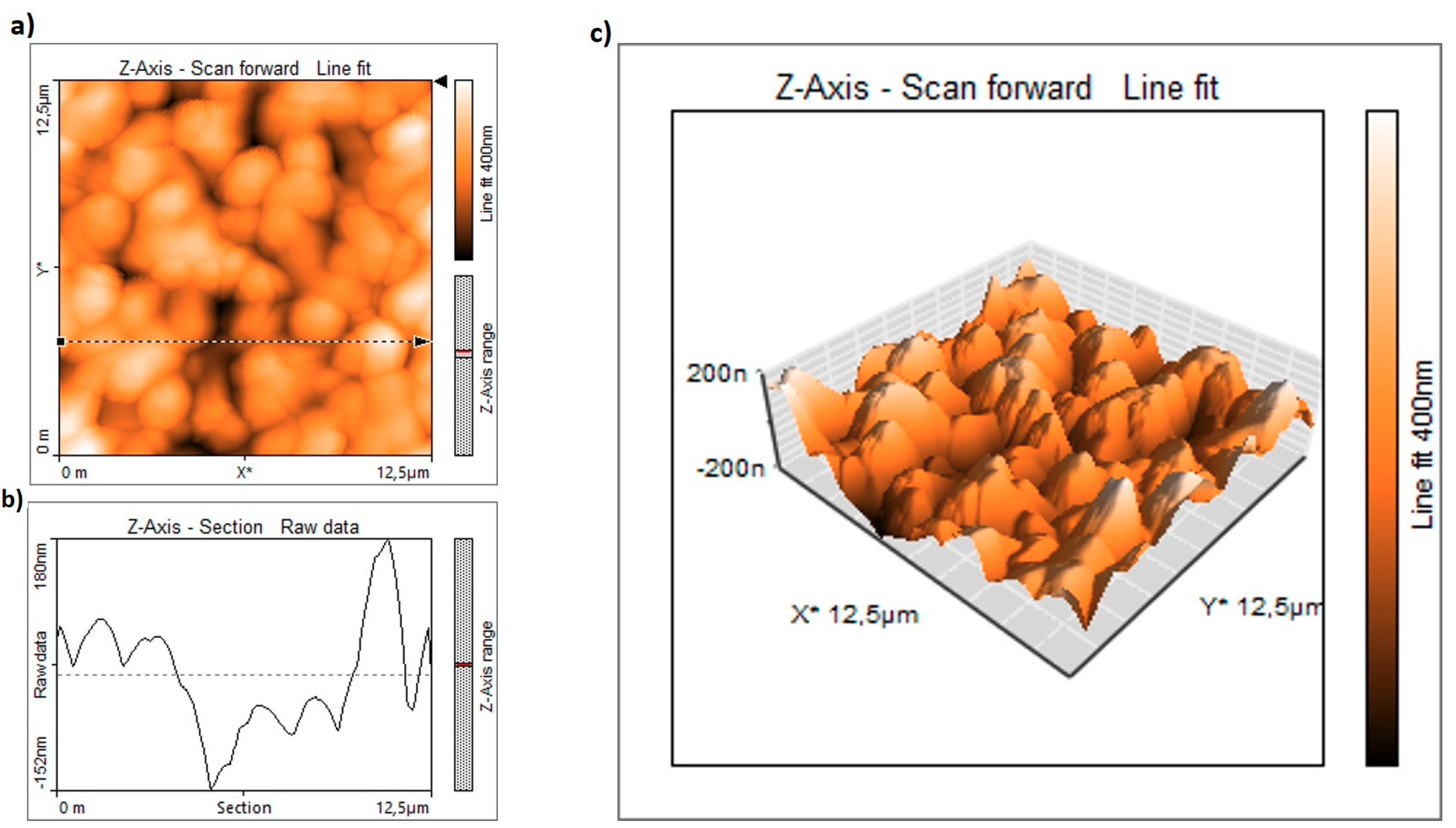
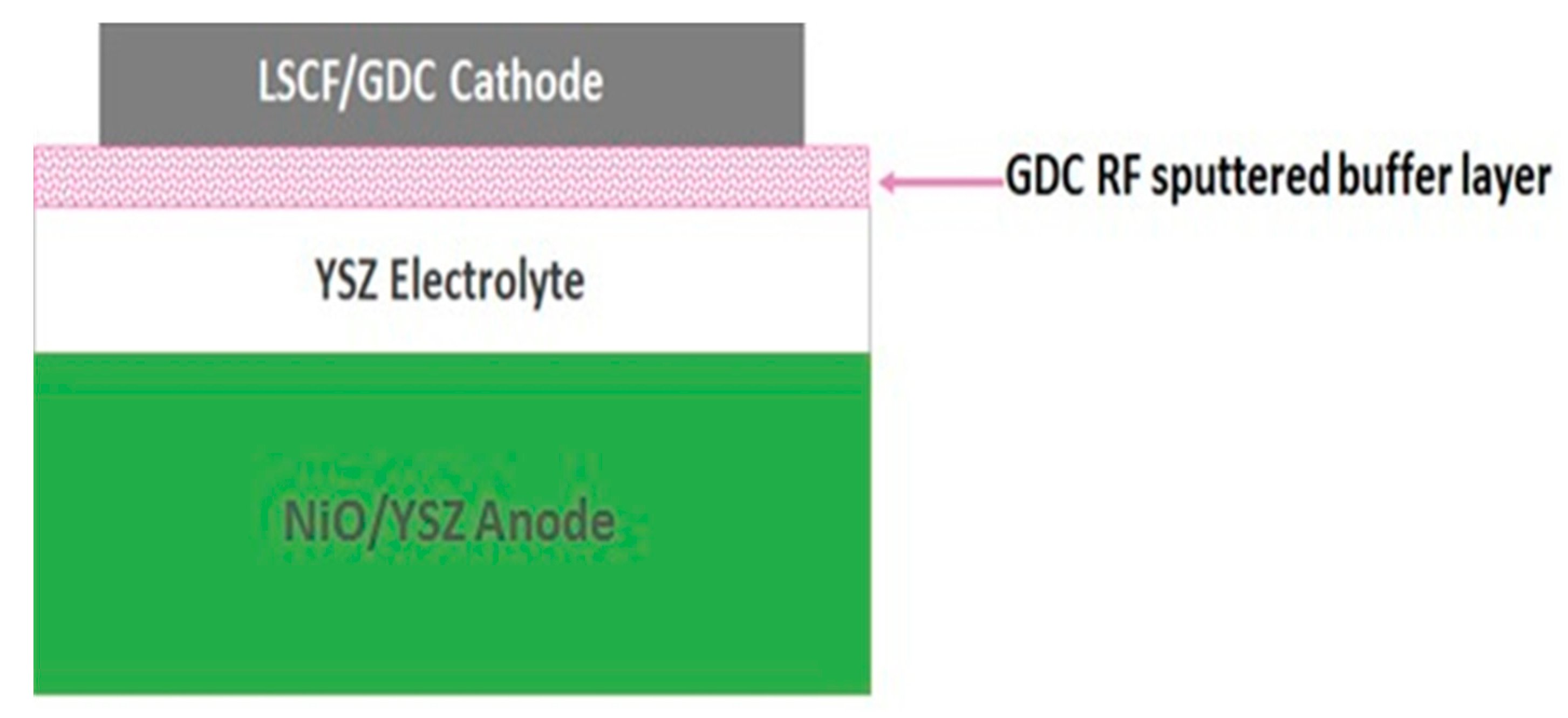
2. Morphological and Crystal Structure Characterization

Before starting the deposition process, the roughness of the YSZ electrolyte was estimated by performing Atomic Force Microscopy (AFM) measurements with a Nanite AFM from Nanosurf in tapping (intermittent contact) mode endowed with a monolithic silicon tip (Tap190Al-G from Budget Sensors, Sofia, Bulgaria) with a force constant of 48 N/m and a resonant frequency of 190 KHz; the AFM head has a 0.3 nm RMS z resolution and 1.5 nm xy resolution. Typical results are shown in Figure 1. The estimated root mean square (RMS) surface roughness is 330 nm in the y growth direction and this gives an inferior limit to the minimum thickness of GDC that has to be deposited on the half cell in order to cover the whole surface homogeneously. For these reasons, the thickness of the sputter-deposited GDC buffer layer has been chosen to be 400 nm.
The barrier layers investigated in the present work were applied on sintered anode supported electrolytes by RF magnetron sputtering (see Section 4). After the sputter-deposition, the as grown samples underwent an annealing process in air up to about 1000 °C, following two different annealing procedures shown in Table 1. The cells have been then completed with a screen-printed cathode layer. The samples obtained using the first procedure in Table 1 are named SPfast, while those made with the second procedure in Table were named SPslow.
XRD measurements have been performed on the samples with the sputter-deposited GDC layer to check the presence of the right stoichiometry and of the eventual preferential growth direction. The XRD profiles have been acquired by means of a Bruker D2 Phaser system using Cu-α radiation (λ = 1.541 Å); the set angular resolution is 0.01 2θ degrees, while the acquisition time is 0.4 s. Figure 2 shows the results of the XRD measurements performed on SPfast and SPslow. Black curves are related to the as grown samples, while red curves are related to annealed samples. The vertical dashed lines show the peaks associated to the bulk GDC cubic phase reflections along the (111), (200), and (220) directions reported in the literature [15]. As expected, in the case of deposition on a polycrystalline substrate, the GDC layer do not present a preferred growth orientation. Moreover, the intensities of all the GDC peaks in the annealed sample are higher than those observed in the as grown samples, giving clear evidence of the importance that the annealing process has in stabilizing the right stoichiometric phase. Another important aspect in Figure 2 is that the XRD profiles of the as-grown sample show GDC (111), (200), and (220) peaks at lower angular positions compared to those present in the annealed sample. Therefore, the lattice parameter calculated from the angular position of these peaks is expected to be larger in the as grown sample.
As it is clear from the figure, also in the case of SPfast samples, the GDC peaks of the as grown specimen appear at lower angles than those of the annealed one, confirming that such an effect is related to the annealed process. Moreover, the crystal axis parameter values along the growth direction of the deposited GDC layers have been evaluated from the 2θ degree angles at which the (111) peak is observed and are reported in the boxes of Figure 2. As expected, along the growth direction axis values of the as grown samples are always larger than the value expected in the bulk case (e.g., 5.412 Å [15]) while those of the annealed samples are very close to the bulk values.
Generally, larger values of the crystalline axis in GDC thin films have been associated to a lack of oxygen [16], and our data seem to confirm that the GDC layer grown at room temperature by sputtering are probably poor in oxygen content.
The annealing process is, therefore, critical because it allows the oxygen to enter the GDC layer obtaining the optimal stoichiometry. We point out that the axis value of the SPslow sample is equal to the bulk value, while the one shown by the SPfast sample is slightly lower. This is an indication of the better structural quality of the SPslow sample associated to the reaching of the optimal oxygen stoichiometry after the annealing process.

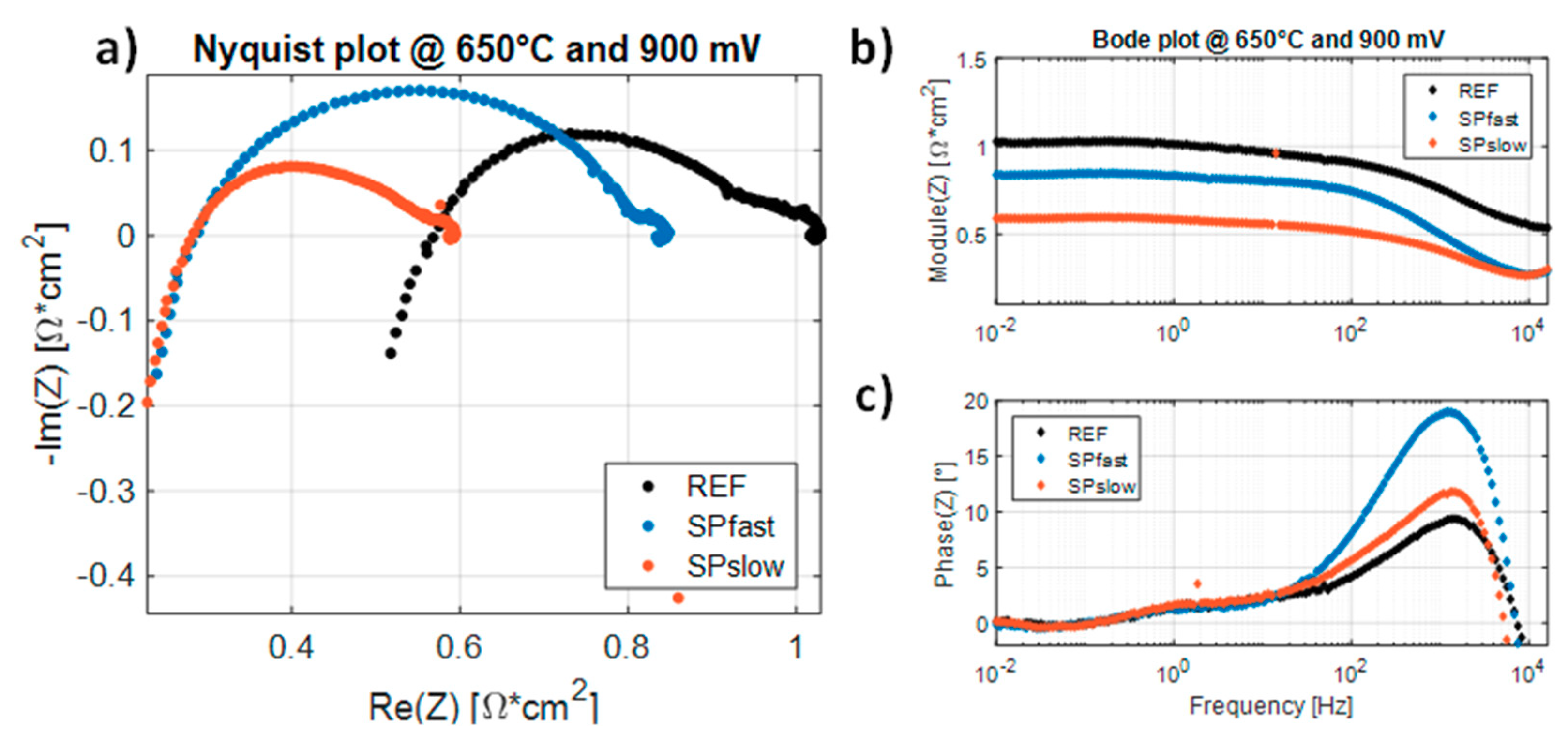
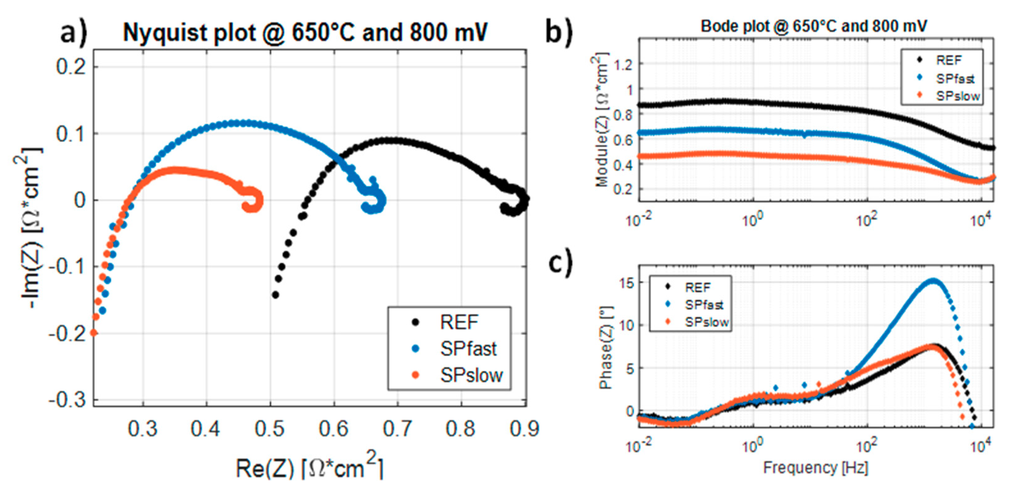
3. Impedentiometric Characterization
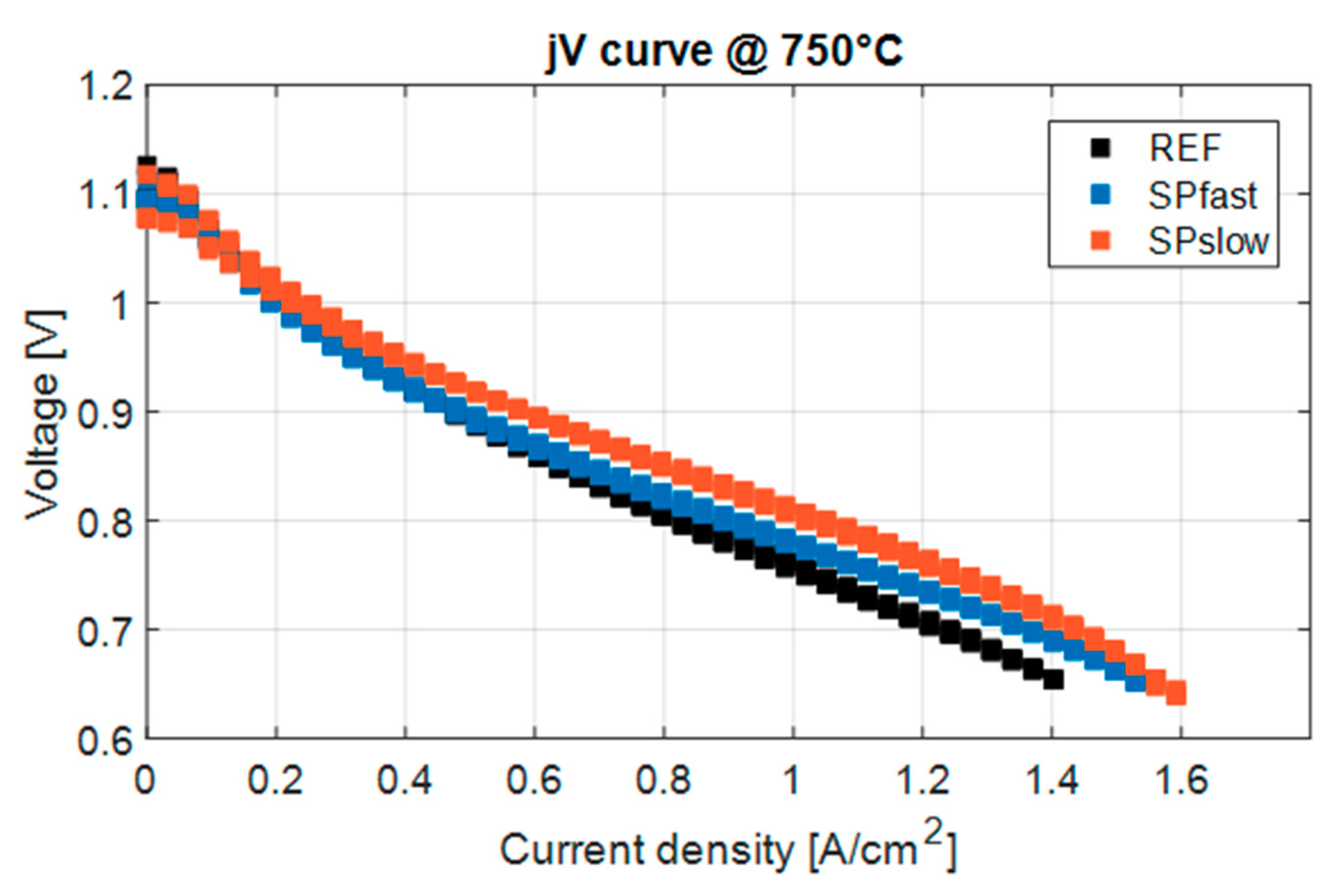
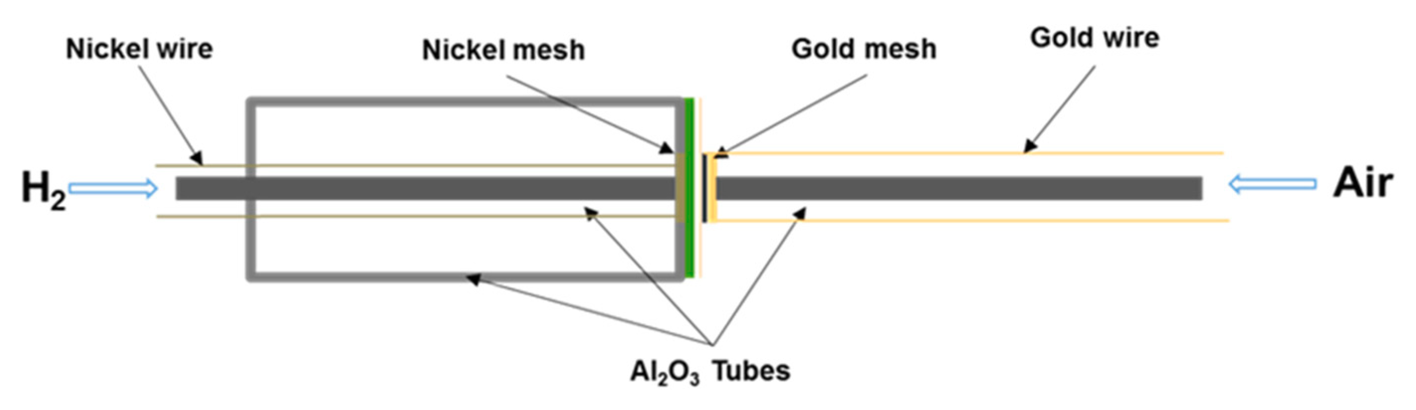
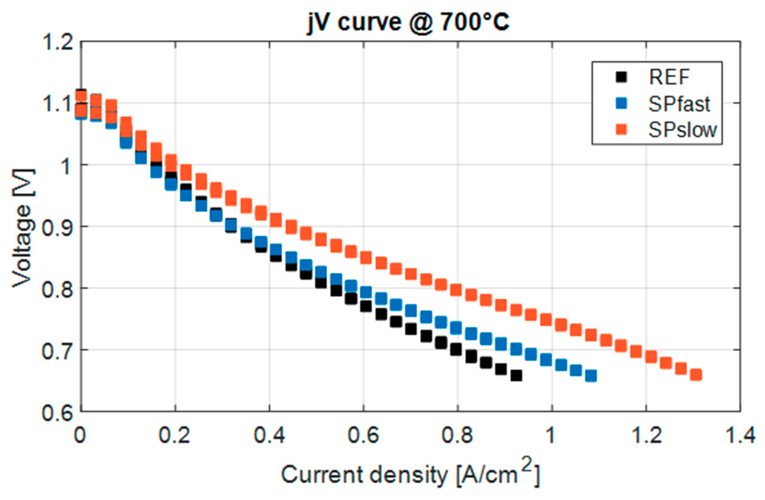
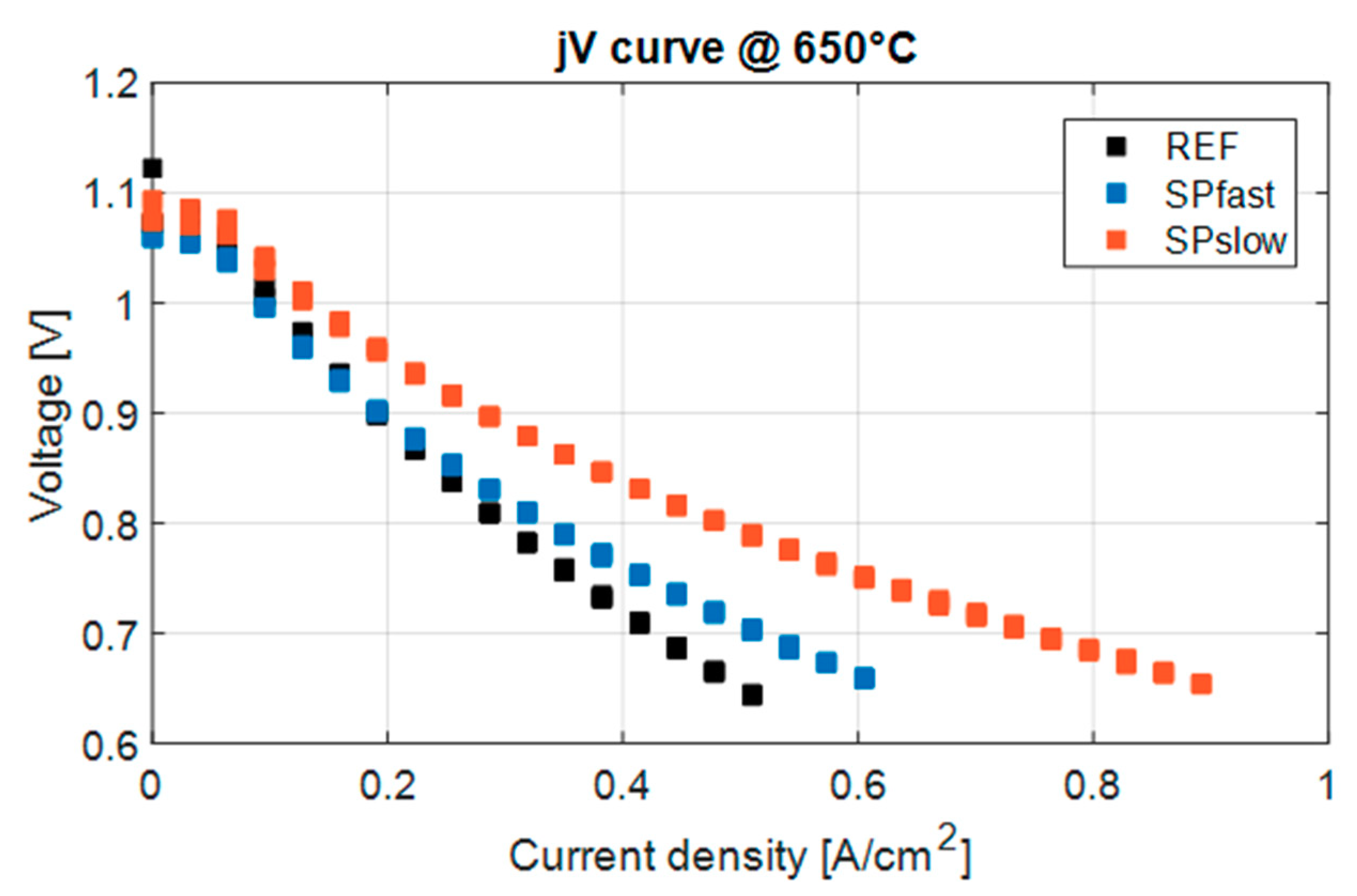
We have compared the performances of the REF, SPfast, and SPslow cells under three different working temperatures that are 750 °C, 700 °C, and 650 °C. The comparison has been performed through the evaluation of jV curves and Electrochemical Impedance Spectroscopy (EIS) measurements.
The testing setup is equipped with only ceramic components. The cell is sealed on an inner large alumina tube where H2 is fed directly on the anode surface by a smaller alumina tube. On the other side, air is fed to the cathode by a small alumina tube. The electrical connection on the electrodes surfaces is provided by gold and Nickel meshes, on the cathode and anode sides, respectively. In order to measure the electrochemical properties, two gold wires are welded on the gold mesh and two Nickel wires are welded on the Nickel mesh. The two meshes are pressed on the surface of the electrodes by applying a mechanical load (250 g/cm2) through springs kept on the cold side of the setup. Electrochemical measurements were performed under the following conditions: the temperature range is 650–750 °C, H2 flow rate is 16 NL/cm2/min, and air flow rate is 40 NL/cm2/min. Measurements were performed using a Potentiostat/Galvanostat with a compliance voltage of 30 V (Autolab/PGSTAT302N by Metrohm Autolab, Utrecht, Netherlands), endowed with a frequency response analyser (FRA) and a booster that increases the maximum current. In Figure 3, a schematic of the setup is shown.
The achieved results are presented and discussed in the following paragraphs.

3.1. jV Curves

The jV curves have been measured at steady-state conditions of voltage and current with the system controlled in potentiostatic mode. The term “steady-state” refers to the operating conditions at which the voltage and current measurements have been performed. It is generally assumed that, to perform these kind of measurements, all the main operating variables (i.e., current, voltage, temperature, pressure, etc.) are kept in steady conditions, which means that their values do not vary much in time (i.e., only oscillate around their average values with a small deviation due to, e.g., devices disturbance and resolution). The results are shown in Figure 4 for a working temperature of 750 °C, in Figure 5 for 700 °C, and in Figure 6 for 650 °C. The reference sample REF is represented with black markers, whereas the SPfast and SPslow samples are sketched with blue and red markers, respectively.
The first observation that can be made with respect to the given jV curves is that both SPfast and SPslow samples perform better than the REF one under all the investigated operating temperatures. However, the SPfast sample shows a less performing behavior if compared to the SPslow sample, as can be argued by observing the slope of the linear region of the jV curve. Nevertheless, the SPslow sample presents a more evident curvature at high current densities (especially at high temperatures), thus implying a possible greater sensitivity to diffusion losses, with respect to the other samples. We point out that the GDC sputter-deposited samples have a much smaller GDC thickness (0.4 μm) than the screen-printed one, resulting in an overall sensible reduction of the total cell thickness.
A quantitative comparison of the behaviors achieved with jV measurements is made with respect to the specific current densities obtained at 900 mV and 800 mV of cell voltage. Such a choice in discussing our jV data allows a more direct comparison to the EIS measurements (see Section 3.2). The measured values are reported in Table 2, also with the percentage deviation with respect to the REF sample (i.e., %Δj).
From the reported values, the qualitative comments given in the previous paragraph are also here confirmed quantitatively. Indeed, with respect to the values achieved with a voltage set-point of 900 mV, the SPfast sample behaves almost as the REF one, whereas the SPslow sample shows an improved performance, from around +20% at 750 °C, up to almost +50% at 650 °C. The results obtained at 800 mV show instead an improvement of both SPfast and SPslow samples, which increases as the temperature decreases (as also observed for 900 mV measurements). Moreover, the maximum increase for SPfast is about +11%, while for SPslow, it is around +67%.
From these preliminary results it can be concluded that a performance improvement is achieved by optimizing the temperature ramp (see Table 1). The increase in performance is also much more evident when operating at lower working temperatures.

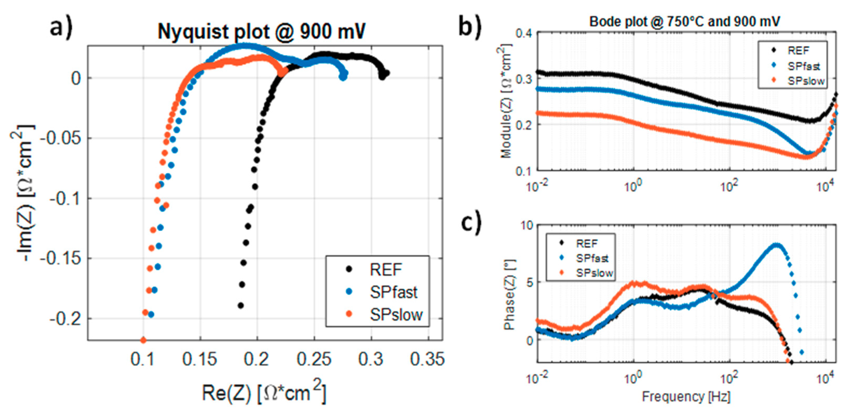
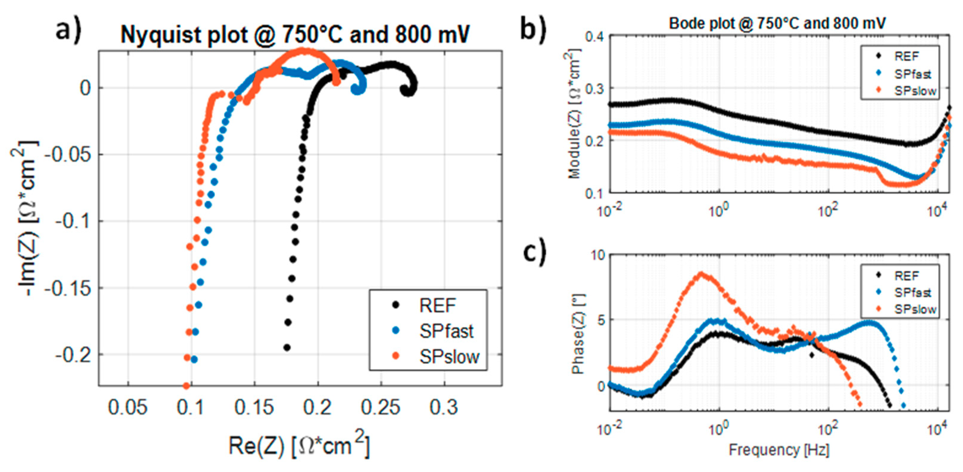
3.2. Electrochemical Impedance Spectroscopy Measurements

Electrochemical Impedance Spectroscopy (EIS) measurement have been performed at the same aforementioned working temperatures (i.e., 750 °C, 700 °C, and 650 °C) and keeping the voltage operation at two different levels, respectively, 900 mV and 800 mV. For each performed measurement both Nyquist and Bode plots are here presented. Each plot presents the REF sample with black markers, the SPfast sample with blue markers, and the SPslow sample with red markers.
The Nyquist and Bode plots at 750 °C and 900 mV are presented in Figure 7. It can be initially observed, from Figure 7a, that both SPfast and SPslow spectra present a high frequency intercept with the real axis RHF much lower than that of the REF sample. This intercept is related to the ohmic resistance of the cell (generally referred to as RΩ). However, the SPfast sample shows a low frequency intercept RLF (or the maximum real value of the impedance if the intercept is not available) greater than that of the SPslow sample and lower than that of the REF one. The difference between the two intercepts RP = RLF − RHF is generally referred to as polarization resistance. Such parameter is low for the SPslow sample, whereas SPfast and REF samples shows a comparable RP.
These results can also be apprised on the Bode plots (Figure 7b,c); indeed, observing the impedance modules, SPfast and SPslow samples have similar high frequency behaviors (i.e., at frequencies higher that 103 Hz), which can be due to inductive effects, while at low frequencies, the SPslow module is the smaller one. This means that, by optimizing the annealing temperature ramp, a better effects on both ohmic and transportation losses can be achieved. Concerning the impedance phase, both REF and SPslow samples show a similar behavior, although the latter is shifted towards higher phase values. The SPfast sample presents instead a superposition with the REF phase at low frequencies, while it has an initial decrement at mid frequencies followed by a rapid increase at high frequencies, which overcomes both REF and SPslow phases. This effect is already visible in the Nyquist plot, which can be associated to an increase in the charge transfer resistance, generally associated to activation losses. This phenomenon can be due to, e.g., a variation in the availability and morphology of the reaction sites. Moreover, this is not in contrast to what is observed with respect to the jV curves, since the better performance of the SPfast curve is observed only at high current density levels (i.e., with respect to the greater SPslow diffusion losses for j > 1.4 A/cm2), whereas the EIS measurements are here analyzed at lower current densities (i.e., with j ≤ 1 A/cm2).
Similar comments can be made for all the other EIS measurements presented in the other figures (from Figure 8, Figure 9, Figure 10, Figure 11 and Figure 12). Indeed, in each Nyquist plot, the SPslow sample shows a lower polarization resistance (if compared with the other samples in the same figure), with small RHF and RLF. In each figure, the SPfast sample always presents larger RP, although with low real axis intercepts, if compared with the REF sample. The comments previously made about Figure 7, also apply to the other Bode plots from Figure 8, Figure 9, Figure 10, Figure 11 and Figure 12.
One particular comment shall be made on the behavior, shown by the SPslow sample at 750 °C and 800 mV. As can be seen in the related Nyquist plot (see Figure 8a), the SPslow spectrum presents a positive imaginary arc at high frequencies (i.e., with real part below 0.15 Ω∙cm2). This behavior is not present in the other plots, and could be related to the presence of high quantity of vapor [17]. Indeed, at 800 mV, the related current density is around 1 A/cm2 (see Table 2), which is the highest current density at which an EIS measurement was performed for these tests. The high current density operation induces a great production of vaporized water, which affect the impedance behavior at high frequencies. A further evident different is observable in the negative arc at low frequencies, which could reasonably be due to the increased vapor transport rate.
The behaviors addressed with respect to all the presented Nyquist and Bode plots are resumed quantitatively in Table 3, Table 4 and Table 5, in terms of RHF, RLF and RP values, respectively. From the reported values, it is worth remarking that both SPfast and SPslow samples show a similar decrease in the RHF intercept. This decrease rises as the temperature diminishes: indeed, the minimum RHF is obtained for both samples at 650 °C, with a maximum reduction of -50% with respect to the REF sample. Nevertheless, it is worth considering that at higher current densities, a greater heat dissipation is induced, with a consequent effect on the ohmic resistance reduction. With respect to the RLF intercept, Table 4 reports a more evident decrease in the low frequency resistance for the SPslow sample with respect to the SPfast one. Indeed, the reduction is more than doubled for the former, reaching around −42% at 650 °C and 900 mV, while the latter settles only to −25% at the same conditions. It can be also noted that, as for the %ΔRHF values, their decrease is fostered by lower operating temperature, but also a reduction in the operating voltage can slightly improve such an effect. Finally, a last comment can be made on the RP values, with a much discordant result for the SPfast and SPslow samples. As mentioned before, the former presents a visible increase in the spectrum, with RP values increasing up +43% at 700 °C and 900 mV, whereas the latter shows instead a reduction in spectrum shape, if compared with the REF sample. Moreover, the increase in the polarization resistance for the SPfast sample is not monotonous, with a maximum at 700 °C and a rapid decrease at lower temperature, while the SPslow sample shows a continuous decrease with temperature reduction.
From the achieved results, it can be concluded that the optimization of the annealing temperature ramp is able to produce a highly positive effect on the high frequency resistance (i.e., ohmic resistance) properties of the SPslow cell (with a maximum reduction of about -50% at 650 °C respect to the REF cell). These effects can be linked to the charge transfer resistance, implying that slower annealing temperature ramps reduce ohmic losses. Such a ramp optimization also improves the low frequency properties at low current density operations, implying that slower annealing temperature gradients reduces the diffusion losses. However, this effect is not achieved at high current densities, since higher slope in the jV curve is visible. This same effect can be observed with respect to the impedance arc size, which is reduced by slower annealing temperature ramps.
It is worth noting that, in principle, the GDC sputter-deposited barrier layer should not affect electrode-related mechanisms (for instance diffusion losses and RP change) as it is part of the electrolyte; nonetheless, the extremely reduced thickness of the GDC barrier layer studied here can give rise to interface phenomena that could have an effect on the electrode behavior. Therefore, further and more detailed analysis is required to explain these observed changes.
All the performed analyses address the importance of the reduced thickness of the GDC sputtered layer, allowed by the use of PVD techniques such as sputtering, which are able to produce GDC thin films with optimal values of the density and the stoichiometry.

4. Samples Preparation

The barrier layers investigated in the present work were applied on sintered anode supported electrolytes by RF magnetron sputtering. These substrates consist of eight µm 8YSZ electrolyte supported on 260 µm Ni/YSZ anode. The diameter of these substrates is 35 mm. For the cells with the sputter-deposited GDC buffer layer, we used an RF magnetron sputtering system equipped with a 150 mm in diameter GDC oxide target (Gd0.1Ce0.9O1.95, Testbourne 99.999% purity). Typical deposition parameters are 400 W power applied at 13 MHz and 2.2 mTorr process gas (Ar) pressure. Previous studies allow measuring the deposition rate and its reproducibility during the time; typical deposition rate is about 30 nm/min and remains the same during the target lifetime [14].
The GDC layers have been sputter-deposited at room temperature on the anode-electrolyte circular half cells 35 mm in diameter, provided by SOLIDpower S.p.A (Mezzolombardo (TN), Italy). After the sputter-deposition, the as grown samples underwent an annealing process in air up to about 1000 °C, in order to obtain the right stoichiometric phase, simultaneously improving the GDC layer adhesion on the half cell surface. Two different annealing procedures have been used in this work, see Table 1. The first one reached the plateau temperature Tplateaux = 1000 °C in about three hours with a heating ramp of 300 °C/h (SPfast samples). In the other one, the samples (SPslow) were first brought at a temperature of 300 °C with a ramp of 1 °C/min, kept at this temperature for an hour and then heated up to 1050 °C with a ramp of 150 °C/h. Both the SPfast and SPslow samples stayed at Tplateaux for 2 h and were then cooled to room temperature with the same procedure. Both cells have been then completed with a screen-printed cathode layer. Cathode inks were prepared by mixing the ceramic powders with a terpineol based vehicle. After screen-printing, the layers were sintered at ca. 1100 °C for 2 h. In Figure 13, a schematic of the complete sputter-deposited cell is shown.
SPslow and SPfast cells have been compared to a standard SOLIDpower S.p.A. cell, labelled REF in the following, which has the same structure shown in Figure 13, unless for the GDC layer that is a screen-printed one. It is authors’ opinion that the sintering process of the cathode does not give particular effects on the sputtered barrier layer; indeed, the annealing treatment performed on the as grown GDC allows reaching the stoichiometric content of oxygen (see XRD profiles in Figure 2). Therefore, no increment in oxygen content is expected. Moreover, the sintering process of the cathode is performed with temperature already experienced by the GDC layer during the annealing treatment. According to these assumptions, further changes in the structure and composition of the barrier layer are not expected.

5. Conclusions

35 mm diameter circular SOFC have been fabricated with a GDC barrier layer sputter-deposited at room temperature and then annealed at temperatures of 1000 °C using different ramp profiles. The AFM and XRD analysis allowed optimizing the ramp profile in terms of the GDC barrier layers structural and stoichiometric properties. The comparison of the electrochemical behavior among the cells with sputtered GDC films and those with screen-printed GDC layers proved better performances of the sputtered cells, giving evidence of the improvements in performance that the use of PVD techniques can give to SOFCs. This is mainly related to the thinner layers that can be realized with these techniques, the enhanced density achieved and the controlled structural quality of GDC layers sputter-deposited. In particular, the cells produced by the optimized temperature ramps have also shown the best electrical performances, giving a strong indication of the tight link between structural quality and electrochemical performances for sputtered GDC barrier layers in SOFC. The results presented in this work also open the way for new and interesting applications of the sputtering process in the industrial production of SOFC. It is worth remarking that the present work consisted in a preliminary investigation of the changes in SOFC performance induced by the sputter-deposition of GDC barrier layers under different annealing temperatures. The results here discussed have been addressed only from an electrochemical point of view, aiming at pointing out which are the evident changes in terms of voltage losses and related physical phenomena. Such results pave the way to further ex-situ analyses, to investigate the morphological and structural changes induced by the considered manufacturing process. Therefore, further analysis is envisaged to study in detail, the fundamental mechanisms at the base of the observed improvements.

Author Contributions

Data curation, N.C., P.P., G.C., C.S., A.U. and V.V.; Investigation, N.C., P.P., A.G., D.M., L.M. and C.P.; Supervision, D.M., L.M. and C.P.; Writing—original draft, N.C. and P.P.; Writing—review & editing, N.C., P.P., D.M., L.M. and C.P.

Funding

This research received no external funding.

Conflicts of Interest

The authors declare no conflict of interest.

References

  1. Santiso, J.; Burial, M. Deposition and characterization of epitaxial oxide thin films for SOFC. J. Solid State Elettrochem. 2011, 15, 985–1006. [Google Scholar] [CrossRef]
  2. Huang, H.; Nakamura, M.; Su, P.; Fasching, R.; Saito, Y.; Prinz, F.B. High-Performance Ultrathin Solid Oxide Fuel Cells for Low-Temperature Operation. J. Electrochem. Soc. 2007, 154, B20–B24. [Google Scholar] [CrossRef]
  3. Knibbe, R.; Hijelm, J.; Menon, M.; Pryds, N.; Sogaard, M.; Wang, H.J.; Neufeld, K. Cathode-Electrolyte Interfaces with CGO Barrier Layers in SOFC. J. Am. Ceram. Soc. 2010, 93, 2877–2883. [Google Scholar] [CrossRef]
  4. Barfod, R.; Hagen, A.; Ramousse, S.; Hendriksen, P.V.; Mogensen, M. Break Down of Losses in Thin Electrolyte SOFCs. Fuel Cells 2006, 6, 141–145. [Google Scholar] [CrossRef]
  5. Yokokawa, H.; Sakai, N.; Horita, T.; Yamaji, K.; Brito, M.E.; Kishimoto, H. Thermodynamic and Kinetic Considerations on Degradations in Solid Oxide Fuel Cell Cathodes. J. Alloys Compd. 2008, 452, 41–47. [Google Scholar] [CrossRef]
  6. Zhou, X.D.; Scarlino, B.; Anderson, H.U. Electrical Conductivity and Stability of Gd- doped Ceria/Y-Doped Zirconia Ceramics and Thin Films. Solid State Ion. 2004, 175, 19–22. [Google Scholar] [CrossRef]
  7. Wang, C.M.; Azad, S.; Shutthanandan, V.; McCready, D.E.; Peden, C.H.F.; Saraf, L.; Thevuthasan, S. Microstructure of ZrO2–CeO2 Hetero-Multi-Layer Films Grown on YSZ Substrate. Acta Mater. 2005, 53, 1921–1929. [Google Scholar] [CrossRef]
  8. Shi, D.Q.; Ionescu, M.; McKinnon, J.; Dou, S.X. Growth Orientation and Surface Morphology of CeO2 Films Deposited by PLD Using Different Deposition Atmospheres. Phys. C 2002, 356, 304–310. [Google Scholar] [CrossRef]
  9. Song, K.; Schmid, H.; Srot, V.; Gilardi, E.; Gregori, G.; Du, K.; Maier, J.; Van Aken, P.A. Cerium reduction at the interface between CeO2 and Y2O3-stabilised ZrO2 and implications for interfacial oxygen non-stoichiometry. APL Mater. 2014, 2, 032104. [Google Scholar] [CrossRef]
  10. Wu, F.; Pavlovska, A.; Smith, D.J.; Culbertson, R.J.; Wilkens, B.J.; Bauer, E.J. Growth and Structure of Epitaxial CeO2 Films on Yttria-Stabilized ZrO2. Thin Solid Films 2008, 516, 4908–4914. [Google Scholar] [CrossRef]
  11. Kerman, K.; Lai, B.K.; Ramanathan, S. Free standing oxide alloy electrolytes for low temperature thin film solid oxide fuel cells. J. Power Sources 2012, 202, 120–125. [Google Scholar] [CrossRef]
  12. Jordan, N.; Assenmacher, W.; Uhlebruck, S.; Haanappel, V.A.C.; Buckremer, H.P.; Stover, D.; Mader, W. Ce0.8Gd0.2O2−δ Protecting Layers Manufactured by Physical Vapor Deposition for IT-SOFC. Solid State Ion. 2008, 179, 919–923. [Google Scholar] [CrossRef]
  13. Klemensø, T.; Nielsen, J.; Blennow, P.; Persson, Å.H.; Stegk, T.; Christensen, B.H.; Sønderby, S. High performance metal-supported solid oxide fuel cells with Gd-doped ceria barrier layers. J. Power Sources 2011, 196, 9459. [Google Scholar] [CrossRef]
  14. Coppola, N.; Carapella, G.; Sacco, C.; Orgiani, P.; Galdi, A.; Polverino, P.; Ubaldini, A.; Maritato, L.; Pianese, C. Investigation of Interface diffusion in Sputter deposited Gd0.1Ce0.9O1.95 thin buffer layers on Y-stabilized Zirconia crystalline substrates for Solid Oxide Cells applications. J. Mater. Sci. Eng. 2018, 7, 482. [Google Scholar] [CrossRef]
  15. Cheng, J.G.; Zha, S.W.; Huang, J.; Liu, X.Q.; Meng, G.Y. Sintering behavior and electrical conductivity of Ce0.9Gd0.1O1.95 powder prepared by the gel-casting process. Mater. Chem. Phys. 2003, 78, 791–795. [Google Scholar] [CrossRef]
  16. Arndt, B.; Noei, H.; Keller, T.F.; Muller, P.; Vonk, V.; Nenning, A.; Opitz, A.K.; Fleig, J.; Rütt, U.; Stierle, A. Structure and Stability of Gd-doped CeO2 Thin Films on Yttria-Stabilized Zirconia. Thin Solid Films 2016, 603, 56–61. [Google Scholar] [CrossRef]
  17. Mohamedi-Boulenouar, F.Z.; Guindet, J.; Hammou, A. Influence of water vapour on the electrochemical oxidation of Hydrogen at the Ni/Zirconia interface. In Proceedings of the Fifth International Symposium on Solid Oxide Fuel Cells SOFC-V; Stimming, U., Singhal, S.C., Tagawa, H., Lenhert, W., Eds.; The Electrochemical Society Inc.: Pennington, NJ, USA, 1997; pp. 441–450. [Google Scholar]
Figure 1. Atomic Force Microscopy image of the NiO/YSZ cermet surface performed on a 12.5 µm2. In (a) the image of the 2D surface topography is shown; in (b) the height profile measured along the line showed by the dashed arrow in (a) is presented; in (c) a 3D reconstruction of the surface topography showed in (a) is displayed. Estimated RMS surface roughness is Ry = 330 nm and Rq = 70 nm.
Catalysts 08 00571 g001
Figure 2. XRD profiles and estimated axis values along the growth direction of all the samples (SPfast in (a) and SPslow in (b)) analyzed in the present study; curves are shifted for clarity. As grown samples XRD are plotted with black lines, while annealed samples are plotted with red lines. The green dashed lines and numbers on top axis show GDC bulk values found in the literature [15].
Catalysts 08 00571 g002
Figure 3. Schematic of the setup used for electrochemical measurements.
Catalysts 08 00571 g003
Figure 4. jV curves of samples REF (black markers), SPfast (blue markers) and SPslow (red markers) measured at 750 °C.
Catalysts 08 00571 g004
Figure 5. jV curves of samples REF (black markers), SPfast (blue markers), and SPslow (red markers) measured at 700 °C.
Catalysts 08 00571 g005
Figure 6. jV curves of samples REF (black markers), SPfast (blue markers), and SPslow (red markers) measured at 650 °C.
Catalysts 08 00571 g006
Figure 7. Nyquist (a) and Bode (b,c) plots of samples REF (black markers), SPfast (blue markers), and SPslow (red markers) measured at 750 °C and 900 mV.
Catalysts 08 00571 g007
Figure 8. Nyquist (a) and Bode (b,c) plots of samples REF (black markers), SPfast (blue markers), and SPslow (red markers) measured at 750 °C and 800 mV.
Catalysts 08 00571 g008
Figure 9. Nyquist (a) and Bode (b,c) plots of samples REF (black markers), SPfast (blue markers), and SPslow (red markers) measured at 700 °C and 900 mV.
Catalysts 08 00571 g009
Figure 10. Nyquist (a) and Bode (b,c) plots of samples REF (black markers), SPfast (blue markers), and SPslow (red markers) measured at 700 °C and 800 mV.
Catalysts 08 00571 g010
Figure 11. Nyquist (a) and Bode (b,c) plots of samples REF (black markers), SPfast (blue markers), and SPslow (red markers) measured at 650 °C and 900 mV.
Catalysts 08 00571 g011
Figure 12. Nyquist (a) and Bode (b,c) plots of samples REF (black markers), SPfast (blue markers), and SPslow (red markers) measured at 650 °C and 800 mV.
Catalysts 08 00571 g012
Figure 13. Schematic of the complete sputter-deposited cell.
Catalysts 08 00571 g013
Table 1. Summary table of annealing treatments.
SampleHeating RampPlateaux Time
SPfastTplateaux = 1000 °C (300 °C/h)2 h
SPslowFrom Troom to T1 = 300 °C (1 °C/min)
T1 maintained for 1 h
From T1 to Tplateaux = 1050 °C (150 °C/h)
2 h
Table 2. Current densities values obtained at 900 mV and 800 mV for all the considered working temperatures.
T = 750 °CT = 700 °CT = 650 °C
V = 900 mVV = 900 mVV = 900 mV
j [mA/cm2]%Δj [%]j [mA/cm2]%Δj [%]j [mA/cm2]%Δj [%]
REF478.00318.60191.10
SPfast477.7−0.06318.4−0.06191.10
SPslow573.1+19.90445.8+39.92286.6+49.97
V = 800 mVV = 800 mVV = 800 mV
j [mA/cm2]%Δj [%]j [mA/cm2]j [mA/cm2]%Δj [%]j [mA/cm2]
REF828.60541.50286.60
SPfast891.8+7.63573.1+5.84318.4+11.10
SPslow1051.0+26.84796.3+47.05477.6+66.64
Table 3. Measured values of the high frequency resistance RHF for the tested samples.
T = 750 °CT = 700 °CT = 650 °C
V = 900 mVV = 900 mVV = 900 mV
RHF [mΩ·cm2]%ΔRHF [%]RHF [mΩ·cm2]%ΔRHF [%]RHF [mΩ·cm2]%ΔRHF [%]
REF219.00342.80567.80
SPfast147.3−32.72194.8−43.15288.5−49.20
SPslow139.4−36.35198.0−42.22283.6−50.06
V = 800 mVV = 800 mVV = 800 mV
RHF [mΩ∙cm2]%ΔRHF [%]RHF [mΩ∙cm2]%ΔRHF [%]RHF [mΩ∙cm2]%ΔRHF [%]
REF199.90334.30558.60
SPfast140.8−29.57191.0−42.85283.4−49.27
SPslow151.8−24.04187.5−43.92275.1−50.75
Table 4. Measured values of the low frequency resistance RLF for the tested samples.
T = 750 °CT = 700 °CT = 650 °C
V = 900 mVV = 900 mVV = 900 mV
RLF [mΩ∙cm2]%ΔRLF [%]RLF [mΩ∙cm2]%ΔRLF [%]RLF [mΩ∙cm2]%ΔRLF [%]
REF313.50526.201029.00
SPfast277.1−11.62458.9−12.79848.6−17.53
SPslow224.6−28.36331.9−36.92593.9−42.28
V = 800 mVV = 800 mVV = 800 mV
RLF [mΩ∙cm2]%ΔRLF [%]RLF [mΩ∙cm2]%ΔRLF [%]RLF [mΩ∙cm2]%ΔRLF [%]
REF276.20457.80901.60
SPfast235.7−14.65365.9−20.07675.8−25.05
SPslow215.4−22.00281.6−38.48483.3−46.39
Table 5. Measured values of the polarization resistance RP for the tested samples.
T = 750 °CT = 700 °CT = 650 °C
V = 900 mVV = 900 mVV = 900 mV
RP [mΩ∙cm2]%ΔRP [%]RP [mΩ∙cm2]%ΔRP [%]RP [mΩ∙cm2]%ΔRP [%]
REF94.50183.50461.10
SPfast129.7+37.28264.1+43.92560.1+21.47
SPslow85.2−9.84133.9−27.01310.3−32.70
V = 800 mVV = 800 mVV = 800 mV
RP [mΩ∙cm2]%ΔRP [%]RP [mΩ∙cm2]%ΔRP [%]RP [mΩ∙cm2]%ΔRP [%]
REF76.30123.50343.00
SPfast94.9+24.43174.9+41.59392.4+14.41
SPslow63.6−16.6594.2−23.76208.2−39.30

