Double-Track Waveguides inside Calcium Fluoride Crystals


1
Université de Bordeaux, CNRS, CEA, CELIA, UMR5107, F-33405 Talence, France
2
Université de Bordeaux, CNRS, ICMCB, UMR5026, F-33608 Pessac, France
*
Author to whom correspondence should be addressed.
Crystals 2020, 10(2), 109; https://doi.org/10.3390/cryst10020109
Submission received: 25 January 2020
/
Revised: 7 February 2020
/
Accepted: 10 February 2020
/
Published: 12 February 2020
(This article belongs to the Special Issue Laser Crystals)
Abstract
:Calcium Fluoride (CaF2) was selected owing to its cubic symmetry and excellent luminescence properties as a crystal of interest, and ultrafast laser inscription of in-bulk double-track waveguides was realized. The guiding properties of these waveguides in relation to the writing energy of the femtosecond pulse are presented. The modified double-track waveguides have been studied by systematic developments of beam propagation experiments and numerical simulations. Furthermore, an adapted model and concepts were engaged for the quantitative and qualitative characterization of the waveguides, particularly for the transmission loss measurements and the three-dimensional refractive index mappings of the modified zones. Additionally, polarization-dependent guiding was investigated.
1. Introduction
The generalized model of bulk damage, in homogenous dielectric materials by ultrafast lasers, involves a combination of nonlinear absorption processes resulting in the excitation and heating of electrons followed by transfer of this heat energy to the surrounding lattice. The deposition of this energy induces, by a variety of mechanisms, refractive index modifications localized over a micrometer-sized volume of the material [1,2,3]. The possibilities of extreme confinement and rapid prototyping of these modifications inside dielectric materials have resulted in the realization of vast ranges of photonic devices, from optical waveguides to more complex photonic circuits. This has been a driving force for a flourishing industrial interest in direct laser writing (DLW) inside dielectric materials in the past two and a half decades [4].
Among its vast applications, DLW has been implemented for the functionalization of laser systems and subsystems in high-repetition-rate laser systems by miniaturizing photonic components, such as monolithic mode-locked waveguide lasers [5,6,7,8]. One of the most important challenges when designing such high-repetition-rate, mode-locked solid-state laser systems is the selection of a gain medium. Although single crystals are generally challenging to grow, when scaling-up diode-pumped laser systems to high power, they are implemented more often than non-crystalline hosts. Crystalline materials, in general, have a lower pump threshold, better Q-switching stability, and better thermal conductivity [9]. Reference [10] provides an excellent review on optical waveguides in crystals describing the writing mechanism and giving an exhaustive overview of the different crystalline materials.
DLW inside cubic crystals enables a more simplified systematic approach to study modifications induced by ultrafast lasers owing to the fact that optical specificities and restrictions of low-symmetry crystal optics are neglected. In relation to DLW inside cubic crystals, for years, a number of works have been reported about DLW inside Y3Al5O12 (YAG) crystals, doped with rare-earth, neodymium (Nd) and ytterbium (Yb) ions to be used as active laser media for realizing ultra-compact, and highly efficient waveguide lasers. Slope efficiencies of 75%, with a so-called parasitic process, and continuous wave output powers of about 5 W were reported by Calmano et al. [11,12,13]. The same group demonstrated a passively Q-switched waveguide laser with a repetition rate of 300 kHz at 300 mW [14]. While this group has been more focused on type II waveguide configurations, the group of Okhrimchuk (Moscow, Russia) has applied DLW on depressed cladding, type III, waveguides inside YAG crystals [15,16,17]. They have demonstrated a microchip type III waveguide laser operating in Q-switched mode and an 11 GHz waveguide laser mode-locked with a single layer of graphene [9]. Besides these two groups, a number of studies and characterizations of waveguides inside rare-earth-doped YAG crystals and ceramics have been demonstrated [18,19,20,21,22,23].
Similarly, Calcium Fluoride (CaF2) is a dielectric crystal which crystallizes into a cubic fluorite structure, space group Fmm3 [24]. The cation positions correspond to the closest packing, and each unit cell has four Ca atoms and eight F atoms. With its high transparency in a broad wavelength range, a low refractive index, and a low phonon energy, CaF2 has been used as commercial optics material from the infrared to the ultraviolet region, such as for windows, and as scintillator crystals for medical imaging applications [25]. Although, it was identified among the first host crystals for active laser media during the 1970s, through time, it has been abandoned due to the need of charge compensation of the Nd3+ ions required to maintain the electroneutrality and the difficulty of its growth. Over the years, other host materials like YAG, or oxide and fluorite glasses were preferred. Recent developments made on ytterbium-doped alkaline-earth fluorides have shown better scalability of the crystal growth as well as comparative spectroscopic and thermo-optical properties [26].
As compared to Yb:YAG, Yb:CaF2 has a larger emission spectrum and thus demonstrated a wider wavelength tuning range and the generation of shorter laser pulses. The nonlinear refractive index is around four times smaller than in the case of YAG [27]. Moreover, the refractive index is similar to conventional glasses, which makes this material suitable as intermediate systems in laser cavities, such as a cavity spacer [28]. Furthermore, Yb:CaF2 has a higher thermal conductivity and laser-induced damage threshold than Yb:YAG, making it a better candidate for high-repetition-rate and high-power laser applications, respectively [29,30]. Due to these advancements and comparative advantages, CaF2, as a “new old laser material” [26], is blooming to become a favorite candidate as a host material for active laser media.
Contrarily, while there are a number of studies about waveguides inside YAG, the study of femtosecond laser written waveguides inside CaF2 has been ignored to date and only a few works have been reported [31]. Recently, Graf et al. categorized the type of modifications inside CaF2 as pearl-chain type [32], which makes it difficult to achieve waveguiding [33]. The only significant recent work was the fabrication of (Yb,Na):CaF2 depressed cladding waveguides produced by DLW technology [34], in which dual-wavelength laser emissions, at 1013.9 nm and 1027.9 nm, with an optical-to-optical conversion efficiency as high as 45.3% and a pulse energy of 0.13 μJ was demonstrated. Just recently, Babu et al. reported double-track cladding inside Nd3+, Y3+ co-doped CaF2 crystals with refractive index, birefringence, transmission loss and micro-luminescence studies as a function of the double-track separation [35] and Guo et al. showed, in a very recent paper, double-track waveguides inside Pr-doped CaF2 crystals with micro-spectroscopy characterizations and refractive index reconstruction [36].
In this paper, we report on the investigation of double-track waveguides achieved inside undoped CaF2 crystals at different pulse energies. To the best of our knowledge, we have demonstrated the first double-track waveguides inside pristine CaF2 samples with comparatively good guiding properties (refer to [37]). Moreover, a detailed description with new characterization approaches of those waveguides is given, which can be reasonably applied in general to any other similar waveguides in crystals or other dielectric materials.
2. Materials and Methods
2.1. Crystal Samples
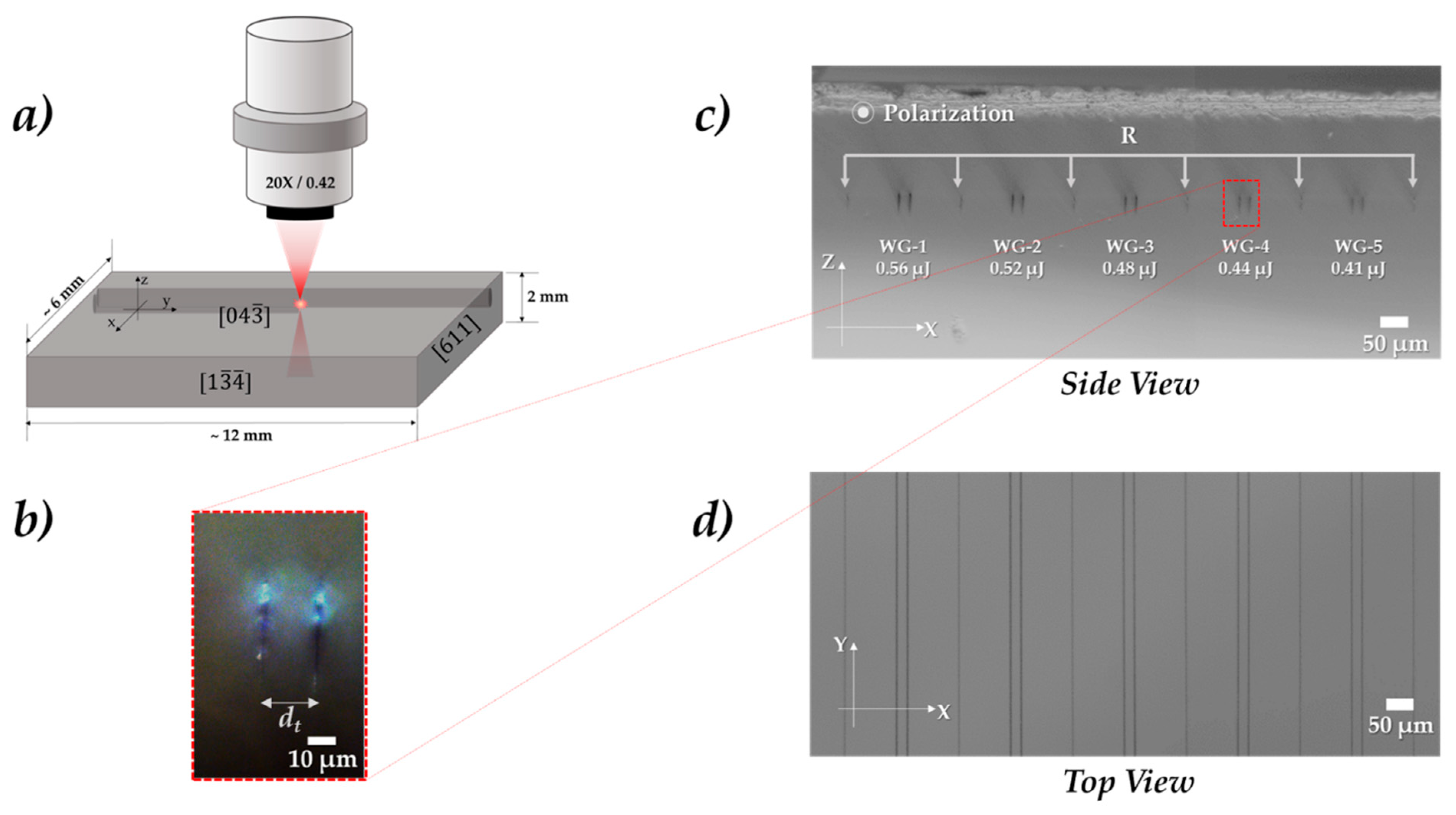
The crystal sample used in the experiments was an undoped CaF2 single crystal with dimensions of x × y × z = (6 × 12 × 2) mm3. The sample had optically polished faces and was randomly cut parallel to the [], [], and [], crystallographic planes along the x, y and z axes, respectively (see Figure 1a). Due to the combined effects of the conical shape of the focused beam and the writing process, which takes place at a certain depth, the DLW process did not access the final few micrometers before the end facets. Therefore, the sample’s end facets, entrance and exit, were polished to optical quality after the writing process. This resulted in 11.06 mm-long double-track waveguides.
2.2. Waveguide Fabrication
Laser pulses are delivered using a Ti:Sapphire regenerative laser amplifier (Coherent, RegA 9000, 250 kHz, at 800 nm) as a femtosecond source with a pulse duration of 170 fs. The pulses were focused using a Mitutoyo Plan Apo objective 20×, 0.42 NA, about 210 µm below the surface of the CaF2 sample while the polarization of the writing beam is kept parallel to the direction of writing—the y-axis (see Figure 1a). The three-dimensional trajectory of the writing tracks is achieved by placing the sample on a slide which is attached to micro-controlled Newport Corporation X-Y-Z stages, XMS50, with a spatial resolution of 40 nm along the predetermined path.
A group of short tracks with various writing speeds and energies were inscribed. The result shows that for speeds exceeding 20 µm/s, there is a strong indication of the pearl-chain type of modification, which could make it impossible to have low-loss waveguiding or even no waveguiding at all [33]. The pearl-chain formation mechanism is not fully understood, observations in glasses attributed this phenomenon to a sudden change in the absorption behaviour due to a temperature rise or to hydrodynamic instabilities [32]. A thorough study in crystals would be necessary to explain its formation and the parameters to avoid it, but this is out of the scope of this work. In order to minimize the probability of such high-loss scatterers in the waveguide structure, we chose a speed of 10 µm/s, attaining maximum overlap between consecutive pulses. This provided an extremely small shift between consecutive beams (about 20 pm) leading to extremely large pulse-to-pulse beam overlap (about 3 × 10⁴ pulses).
In addition, we observed that the pulse energy plays a more influential role for the thresholds of modification and microcrack formation than the writing speed. This can be evidenced from the fact that the given focusing conditions and the repetition rate of the laser source result in an athermal regime of writing [38]. It was identified that an energy of 0.33 µJ corresponds to the threshold of modification, while an energy of 0.61 μJ and above results in microcracks, which can be due to the porosity of micro-sized CaF2 amorphous formations that appear at the core of the submicron-sized damage filaments [39,40].
Thus, once the thresholds of modification and crack formation had been identified, five double-track waveguides were inscribed with energies per pulse from 0.41 to 0.56 µJ. This covers a range between 25 % above the damage threshold (0.33 µJ) and slightly below the crack formation energy of 0.61 µJ, approximately. The distance between adjacent tracks was kept constant at 20 µm for all the waveguides (see Figure 1b). The five 20 µm double-tracks are designated as WG-1, WG-2, WG-3, WG-4, and WG-5, respectively, for 0.56 µJ, 0.52 µJ, 0.48 µJ, 0.44 µJ, and 0.41 µJ pulse energies, respectively, and are separated by 200 µm. In addition, a single track is also inscribed at a 0.52 µJ pulse energy in between the waveguides, which is used as a reference for the characterization experiments (see Figure 1c,d).
2.3. Guided Modes Profiles: Measurement and Simulations
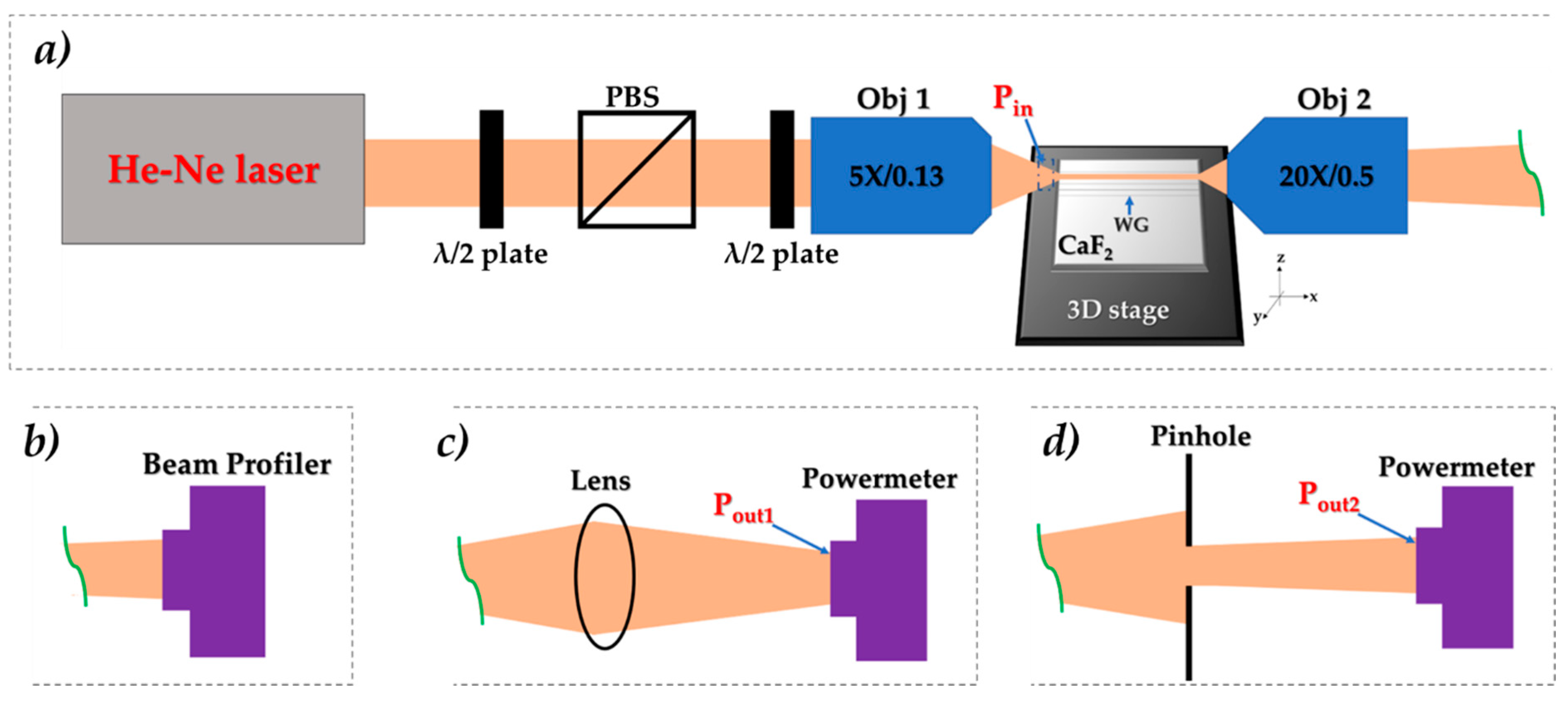
The near-field guided mode profiles were observed using a simple free-space beam (end) coupling setup. The source is a linearly polarized He-Ne laser at 632.8 nm wavelength with a circular Gaussian mode and a measured M-squared (M2) value of 1.07. A half-wave (λ/2) plate in combination with a polarization beam splitter, PBS, adaptably controls the injected power with parallel (p-) polarized (with respect to the setup table) light just after the PBS. A second half-wave (λ/2) plate is used to control and match the polarization of the injected beam into the waveguides. Because of the observed weak guiding of light by the waveguides, a low numerical aperture (NA) objective, an Olympus Neo SPlan 5×, with NA = 0.13, is used to inject the source, resulting in an optimum beam waist (~15 µm) as compared to the horizontal (x) dimension of 20 µm of the double-track waveguides. The effective NA of the injected beam is measured to be 0.030, which is due to a smaller input beam diameter compared to the objective aperture. This results in a better NA matching between the injected beam and the guided modes of the waveguides. The sample is placed on a three-dimensional (3D) translation stage with linear x, y and z translations in combination with the rotary translations (θ, φ) to cover all points at a micrometer-level alignment. The near-field mode profile at the exit facet of the sample is sharply imaged by an Olympus UPlanFLN 20× with NA = 0.5 onto a beam profiler, the sensor of a CCD camera (Thorlabs, BC106-VIS).
For the setups shown in Appendix A (Figure A1), we assumed the observed guided mode has a Gaussian distribution and the most accurate way of applying mode field diameter (MFD) calculation is by considering the boundary at the more generalized criterion in which the intensity drops to 1/e2 of the maximum intensity, commonly also known as D4σ method. Thus, the power density distribution (PDD) of the guided mode, Ig, is given as:
where Ig is the guided intensity at coordinates r, θ; Pg,tot is the total power of the guided mode; ωx and ωz are the beam radii of the guided mode along the horizontal (x) and vertical (z) axes of the side view, respectively; and r, θ are polar coordinates.
In addition to the mode injected by the given HeNe Gaussian beam, all the modes supported by the waveguides can be identified numerically using a Finite-Difference Time-Domain (FDTD) solver. One of the numerical computation methods to solve the modes of the waveguides is using Eigen solutions of the 3D Maxwell’s equations (refer to [41], [42]). In our case, a Finite Difference Eigenmode (FDE) solver of Lumerical MODE Solutions, from Lumerical Inc., is applied to 3D refractive index changes (RIC) of the double-track waveguides to calculate the mode field profiles of modes at a cross-sectional mesh of the waveguides. Determination of the 3D RIC of the double-track waveguides was performed by measuring the side and top-view 2D optical path difference (OPD) map of the waveguides obtained from a special type of quantitative phase imaging (QPI) called quadri-wave lateral shearing interferometry (QWLSI). The OPD is measured at the cross-sectional layer with commercially available equipment (SID4Bio from PHASICS Inc.), having a spatial sampling of 250 nm, plugged onto a lateral video port of an inverted microscope (Zeiss Axiovert 200 M Microscope, Göttingen, Germany). The sample is illuminated with a white-light centered around 550 nm with condenser illumination of effective NA of 0.05, and the transmitted light is collected using an oil immersion objective of magnification 100× with NA = 1.3. For details about the QWLSI technique, see [43,44,45].
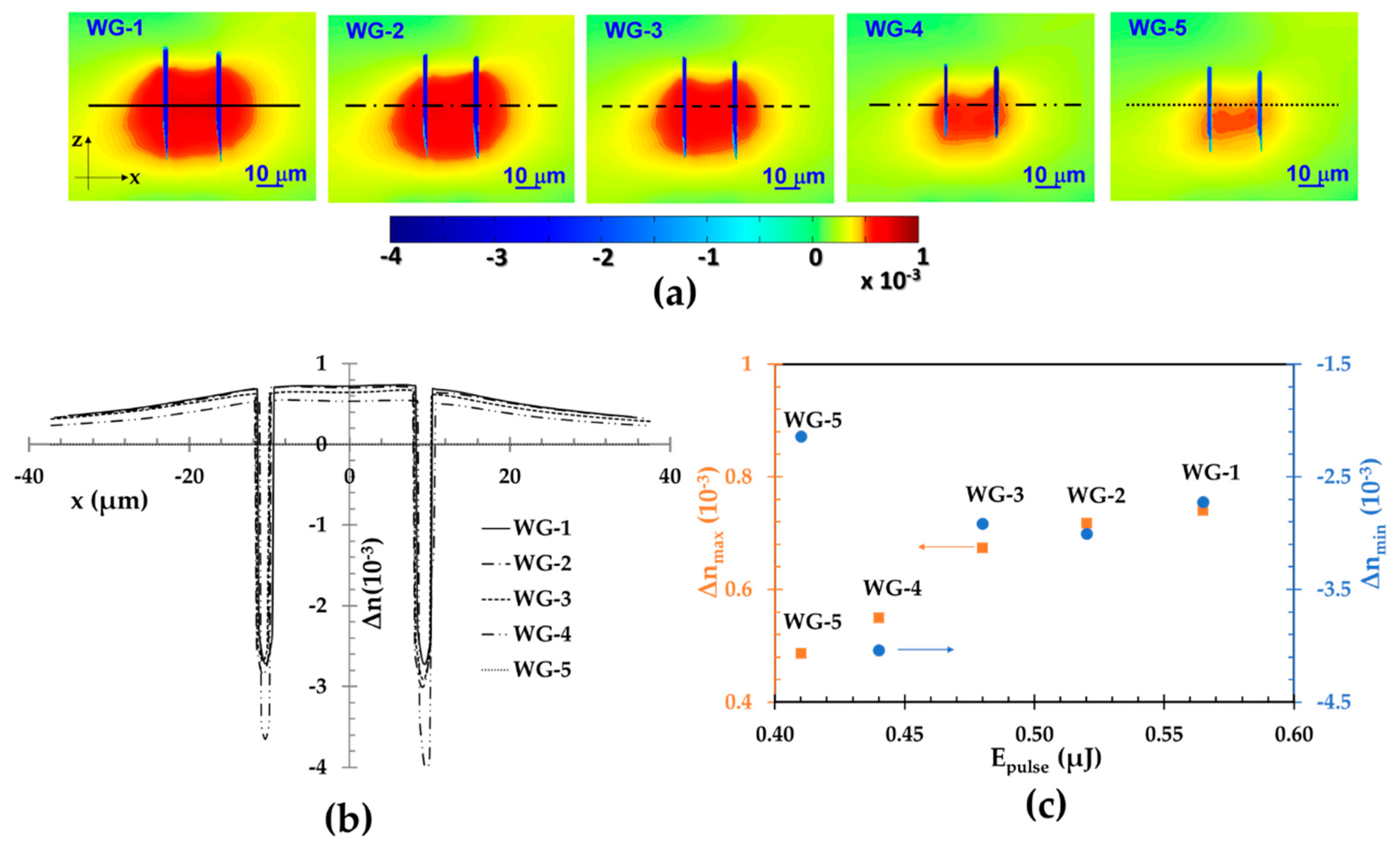
Due to the structural symmetry along the y-axis, the 3D RIC profile of the waveguides is the lateral repetition of the longitudinal 2D RIC extending throughout the entire length of the waveguides (see Figure 2a). As it can be derived from Figure 2b,c, the RIC values for the five waveguides are in the range of around 10-3 in the vicinity of the tracks to around −4×10⁻³ along the tracks. The maximum value of RIC of the waveguides is directly proportional to the writing energy, Epulse (µJ). Contrarily, the minimum RIC of the waveguides shows no particular trend, indicating that in addition to the writing energy, intrinsic crystallographic modifications along the modified tracks play a major role for the negative refractive index change.
2.4. Transmission Loss Measurement Setup
Most of the previously reported works on double-track waveguides inside crystals, which implement free-space beam coupling setups, apply the mode field overlap integral to determine the transmission loss between the input beam and the waveguide [46,47,48]. While the major drawback of this assumption for double-track crystalline waveguides is that the RIC incurred is not only confined in the region between tracks but also extends in the side lobes of the tracks (see Figure 3a). Therefore, the mode matching conditions of such waveguides require rather more complex matching considerations than fiber-like mode matching.
In our case, due to the aforementioned complexity of determining how the mode field overlapping occurs between the injected beam and the waveguide, the total injected light is assumed as the sum of measured guided and modelled uncoupled mode profiles. The uncoupled mode profile is assumed to be predominantly on the edge of the waveguides and is trapped in the vicinity of the tracks spanning from the entry to the exit facets owing to the fact that the RIC extends on the immediate side lobes of the tracks (refer to Appendix A).
3. Results and Discussion
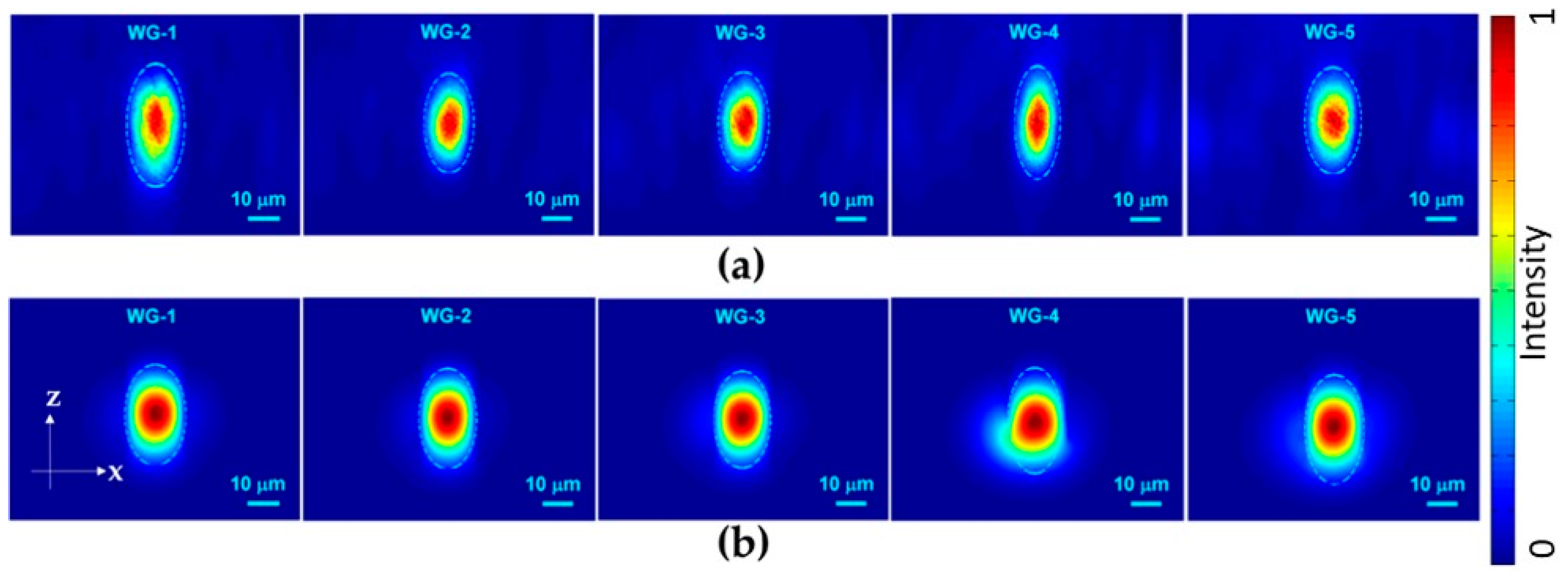
Once the 3D RIC is obtained, the 3D spatial mappings of refractive indices are realized by simply adding the refractive index of CaF2 at 632.8 nm, n = 1.4348, over the entire ensemble of 3D RIC values. Thus, using Import object for the (n,k) data tool in the Lumerical software, the possible TE and TM eigen modes propagated are simulated inside each waveguide. The numerical simulation results indicated that the waveguides are multimodal. The experimentally observed guided modes are highly consistent with the simulation results, see Table 1. The corresponding simulation results are given in parentheses.
Furthermore, the overlap integral between the assumed HeNe beam (circular Gaussian mode with a beam waist of 7.5 µm at 632.8 nm) and the fundamental mode of the numerically simulated modes showed that the overlap is at least 85%, while it is less than 1% for the consecutive higher-order TE/TM Eigenmodes. This proves that the excited modes in both, guiding and transmission loss experiments, are predominantly Gaussian modes for all the waveguides. In addition, the simulated effective numerical aperture ranges between 0.041, for WG-1, to 0.033, for WG-5, which exceeds the effective NA of the injected beam in our experiment, 0.030.
Consequently, the guiding setup has produced an almost “perfect” NA matching and high coupling efficiency. Indeed, we expect a very good mode matching since the NAs of the waveguides and of the injected sources are very similar; mode mismatch is thus neglected. The insertion losses due to Fresnel reflections from both entrance and exit faces lead to a correction per interface of 0.9683, namely to 0.14 dB per interface. Note that neglecting the mode mismatch consequently leads to a slight over-estimation of the reported propagation losses of our waveguides. Therefore, most of the unguided light should be the result of a mismatch between the ellipticity of the PDD of the guided mode and the injected circular source beam, which is not explainable by considering only a single equivalent value like an effective refractive index or the error due to micrometer-level control of the injection optics. Note that the applied method to determine the propagation losses is insensitive to the absolute value of the coupling losses.
As it can be observed from the images in Figure 3, the obtained profiles are highly elliptical for the injected circular beam. The simulated fundamental modes have an overall ellipticity below 0.55, while we obtained ellipticity below 0.56 for the guiding experiment. The modes simply correspond to the injected circular Gaussian modes that are constricted by the tracks, stretched along the z-axis and squeezed along the x-axis. This is evidenced by the leaked mode at the bottom-left corner track of WG-4 since the 3D RIC measurement represents the measurement only at a single layer for the track that extends throughout the whole guiding structure (compare Figure 2a and Figure 3b). On the other hand, other experimental and simulation runs for similar energies and the same writing speed, 10 µm/s, showed that an increase of the distance between the tracks does not necessarily result in Gaussian fundamental modes. This is due to the fact that a change in the distance of the double-tracks modifies the entire longitudinal 2D RIC distribution between the tracks.
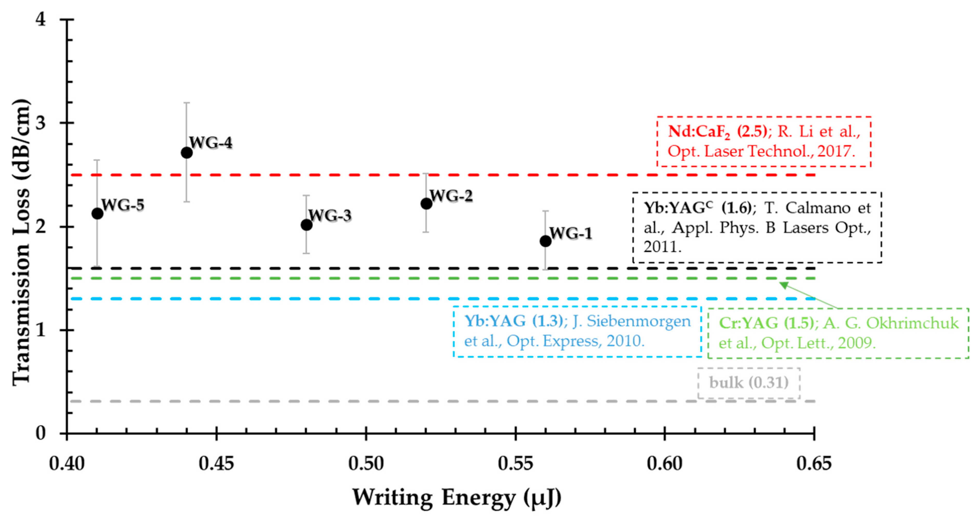
The five waveguides of undoped CaF2 exhibited a transmission loss between 1.9 dB/cm (WG-1) to 2.7 dB/cm (WG-4), while the pristine crystal transmission loss is 0.31 dB/cm at 633 nm. Figure 4 shows that the results are within the range of some previously reported transmission loss measurements of waveguides in YAG crystals, which were 1.3 dB/cm for Yb:YAG [11], 1.5 dB/cm for Cr:YAG [17] and 1.6 dB/cm was reported for Yb:YAG ceramics [49]. In addition, the superficial cladding waveguides written inside Nd:CaF2 have been reported with a transmission loss of 2.5 dB/cm [31].
As it was described above, the unguided beam model simply considers free bulk propagation subtracted by the confinement of the low numerical aperture rays of laser light. However, the sub-micrometer size of the negative RIC tracks along the x-axis is on the same order of magnitude as that of the source wavelength. This introduces significant near-field diffraction effects of the tracks in the immediate vicinity of the waveguides [50]. Therefore, the uncoupled laser light model, in Equation (A1), results in an overestimation of the transmission losses in comparison to the real losses of the waveguides. Thus, a more complex and realistic model would improve the transmission loss measurement results reported in this work.
Previous studies have shown that stress-induced birefringence and selective guiding of only one polarization state has been reported in YAG crystals and ceramics [11,49,51,52,53,54]. Similarly, we have observed that for all five waveguides, only the polarization parallel to the damage tracks was guided while exhibiting a polarization extinction ratio (PER) between 15 dB to 20 dB, i.e. 1:32 to 1:100 parts for the beam polarized perpendicular to the double-tracks.
So far, the polarized white-light 3D RIC measurements and phase retardance measurements of light along the waveguides showed little to no birefringence in the case of these conventional double-track waveguides inside the CaF2 crystal. A recent study by Qi et al. on polarization-dependent guiding performances of LiNbO3 crystals presented similar results. Propagating waves with the polarization parallel to the tracks is guided, i.e., the TE modes for vertical double lines are guided, while the polarization perpendicular to the double lines show very low transmission [55]. Similarly, in our case, the experimental results showed low transmission of the TM modes, i.e., for perpendicular polarization of the injected beam with respect to the double-tracks. This is mainly due to the structural asymmetry of the modified tracks along the horizontal (x) and vertical (z) axes, which leads to polarization-dependent guiding properties and, consequently, asymmetrical transmission loss.
4. Conclusions
The waveguiding properties of double-track waveguides inside CaF2 were investigated with a free-space beam coupling setup. The numerical simulation of the DLW-induced refractive index changes showed a multimode waveguide, while the near-field fundamental modes are in excellent agreement with the near-field guided mode profiles of the experiment. The guided modes follow a Gaussian elliptical profile with an ellipticity lower than 60%. We have developed a simple model of the uncoupled laser light profile to estimate the possible losses of double-track waveguides inside crystals. The maximum transmission losses were determined according to this approach, which results in an over-estimation of the transmission losses of the waveguides. Despite that, the transmission losses of the five CaF2 double-track waveguides are within the range of previously reported transmission loss measurements inside similar crystals. Furthermore, a study of the polarization-dependent guiding of the waveguides showed that the waveguides act almost like perfect polarizers.
Author Contributions
Conceptualization, L.C. and I.M.-H.; Methodology, L.C., Y.P. and I.M.-H; Validation, Y.P, L.C., and I.M.-H.; Formal Analysis, W.G. and L.C.; Investigation, W.G and L.C.; Data Curation, W.G. and L.C.; Writing – Original Draft Preparation, W.G.; Writing – Review & Editing, L.C., Y.P. and I.M.-H.; Supervision, L.C. and I.M.-H.; Project Administration, I.M.-H.; Funding Acquisition, L.C. and I.M.-H. All authors have read and agreed to the published version of the manuscript.
Funding
This work was supported by the Association Nationale de la Recherche et de la Technologie (ANRT) under Cifre program and Amplitude Laser Group and by the French State, managed by the French National Research Agency (ANR) in the frame of “the Investments for the future” Programme IdEx Bordeaux – LAPHIA (ANR-10-IDEX-03-02).
Acknowledgments
The authors thank Patrick Mounaix from the Laboratoire de l’Intégration du Matériau au Système (IMS – UMR5218) in Bordeaux, France, for providing the CaF2 crystal sample.
Conflicts of Interest
The authors declare no conflict of interest.
Abbreviations
| DLW | Direct Laser Writing |
| YAG | Yttrium Aluminum Garnet |
| CaF2 | Calcium Fluoride |
| NA | Numerical Aperture |
| DF | Dark-Field |
| BF | Bright-Field |
| WG | double-track Waveguide |
| HeNe | Helium–Neon |
| λ/2 plate | Half-wave Plate |
| CCD | Charge-Coupled Device |
| MFD | Mode Field Diameter |
| PDD | Power Density Distribution |
| FDTD | Finite-Difference Time-Domain |
| FDE | Finite Difference Eigenmode |
| 3D | Three-Dimensional |
| RIC | Refractive Index Change |
| 2D | Two-Dimensional |
| OPD | Optical Path Difference |
| QPI | Quantitative Phase Imaging |
| QWLSI | Quadri-Wave Lateral Shearing Interferometry |
| Epulse | Writing Energy per Pulse |
| TE | Transverse Electric |
| TM | Transverse Magnetic |
| dB | decibel |
| PER | Polarization Extinction Ratio |
| Gm | guided mode |
| Fp | free propagation of beam |
| Tf | Fresnel Transmission Coefficient |
Appendix A
The uncoupled light mode profile is modelled as the free propagation of the beam inside the pristine crystal while assuming that all of the “top hat”, lowest numerical aperture rays of light, vanishing according to the guided Gaussian beam at the exit facet. Thus, the normalized PDD of the modelled uncoupled mode is the normalized guided mode profile, PDDgm, subtracted from the normalized PDD of free propagation of the beam, PDDfp, at the exit facet. This is represented as:
where Iu is the uncoupled intensity at coordinates r,θ; Pu,tot is the total power of the uncoupled laser light; ωu is the free space propagation beam radius at the end facet of the sample, which is given as ωo; ωo is the beam waist of the HeNe source (~7.5 µm); lc and ZR are the length of a waveguide and the Rayleigh length, respectively; ωx and ωz are the beam radii of the guided mode in the horizontal (x) and vertical (z) axes of the side view, respectively; r and θ are polar coordinates in the side view (xz-plane); the surface normalisation results here from the resulting surface obtained at the exit facet as the circular area of the diverging free propagation mode minus the elliptical area of the guided mode.
Figure A1.
(a) Free-space beam coupling setup implemented for: (b) beam profile experiment; (c) and (d) case 1 and case 2 of transmission loss experiments, respectively.
Figure A1.
(a) Free-space beam coupling setup implemented for: (b) beam profile experiment; (c) and (d) case 1 and case 2 of transmission loss experiments, respectively.

According to the setup shown in Figure A1c,d, for each waveguide, two sets of power measurement are performed. For the case 1, all of the guided and uncoupled light is collected by the lens onto the powermeter (see Figure A1c). The measured power is given as follows:
where ζg and ζu are the PDD models of guided and uncoupled angular profiles derived from Equations (1) and (A1), respectively. Tf1 is the product of the transmission coefficients of the sample (Fresnel), the collecting objective, and the lens. αg is the transmission loss of the waveguides in 1/cm. αu is the transmission loss of the pristine crystal or unguided mode and equals 0.06/cm. Similarly, for case 2, all of the guided and only part of the uncoupled light is collected onto the powermeter (see Figure A1d). The measured power is given as follows:
where rpin is the radius of the pinhole. Tf2 is the product of the transmission coefficients of the sample (Fresnel) and the collecting objective. As shown in Figure A1a, the input power was measured just before the input facet of the sample. Thus, it is given as the sum of the guided and uncoupled light as:
where Tf is the Fresnel transmission coefficient.
Therefore, given the linear system of the two Equations (A2) and (A3) supported by experimental measurements Pout1 and Pout2 and taking into account the closing relationship in Equation (A4), one can extract the parameter αg.
References
- Eaton, S.M.; Cerullo, G.; Osellame, R. Fundamentals of Femtosecond Laser Modification of Bulk Dielectrics BT—Femtosecond Laser Micromachining: Photonic and Microfluidic Devices in Transparent Materials; Osellame, R., Cerullo, G., Ramponi, R., Eds.; Springer: Berlin, Germany, 2012; pp. 3–18. [Google Scholar]
- Gattass, R.R.; Mazur, E. Femtosecond laser micromachining in transparent materials. Nat. Photonics 2008, 2, 219–225. [Google Scholar] [CrossRef]
- Tan, D.; Sharafudeen, K.N.; Yue, Y.; Qiu, J. Femtosecond laser induced phenomena in transparent solid materials: Fundamentals and applications. Prog. Mater. Sci. 2016, 76, 154–228. [Google Scholar] [CrossRef]
- Malinauskas, M.; Žukauskas, A.; Hasegawa, S.; Hayasaki, Y.; Mizeikis, V.; Buividas, R.; Juodkazis, S. Ultrafast laser processing of materials: From science to industry. Light Sci. Appl. 2016, 5, e16133. [Google Scholar] [CrossRef] [PubMed] [Green Version]
- Lagatsky, A.A.; Choudhary, A.; Kannan, P.; Shepherd, D.P.; Sibbett, W.; Brown, C.T.A. Fundamentally mode-locked, femtosecond waveguide oscillators with multi-gigahertz repetition frequencies up to 15 GHz. Opt. Express 2013, 21, 19608. [Google Scholar] [CrossRef] [PubMed] [Green Version]
- Choudhary, A.; Lagatsky, A.A.; Kannan, P.; Sibbett, W.; Brown, C.T.A.; Shepherd, D.P. Diode-pumped femtosecond solid-state waveguide laser with a 49 GHz pulse repetition rate. Opt. Lett. 2012, 37, 4416. [Google Scholar] [CrossRef] [PubMed] [Green Version]
- Mary, R.; Brown, G.; Beecher, S.J.; Torrisi, F.; Milana, S.; Popa, D.; Hasan, T.; Sun, Z.; Lidorikis, E.; Ohara, S.; et al. 1.5 GHz picosecond pulse generation from a monolithic waveguide laser with a graphene-film saturable output coupler. Opt. Express 2013, 21, 7943. [Google Scholar] [CrossRef]
- Okhrimchuk, A.G.; Obraztsov, P.A. 11-GHz waveguide Nd:YAG laser CW mode-locked with single-layer graphene. Sci. Rep. 2015, 5, 11172. [Google Scholar] [CrossRef] [Green Version]
- Cahill, D.G.; Pohl, R.O. Lattice vibrations and heat transport in crystals and glasses. Annu. Rev. Phys. Chem. 1988, 39, 93–121. [Google Scholar] [CrossRef]
- Chen, F.; de Aldana, J.R.V. Optical waveguides in crystalline dielectric materials produced by femtosecond-laser micromachining. Laser Photon. Rev. 2014, 8, 251–275. [Google Scholar] [CrossRef]
- Siebenmorgen, J.; Calmano, T.; Petermann, K.; Huber, G. Highly efficient Yb:YAG channel waveguide laser written with a femtosecond-laser. Opt. Express 2010, 18, 16035. [Google Scholar] [CrossRef]
- Calmano, T.; Ams, M.; Dekker, P.; Withford, M.J.; Kränkel, C. Hybrid single longitudinal mode Yb:YAG waveguide laser with 16 W output power. Opt. Mater. Express 2017, 7, 2777. [Google Scholar] [CrossRef]
- Calmano, T.; Siebenmorgen, J.; Paschke, A.-G.; Fiebig, C.; Paschke, K.; Erbert, G.; Petermann, K.; Huber, G. Diode pumped high power operation of a femtosecond laser inscribed Yb:YAG waveguide laser [Invited]. Opt. Mater. Express 2011, 1, 428. [Google Scholar] [CrossRef]
- Calmano, T.; Paschke, A.; Müller, S.; Kränkel, C.; Huber, G. Q-Switched Operation of a fs-Laser Written Nd:YAG/Cr4+:YAG monolithic waveguide laser. Lasers Sources Relat. Photonic Devices 2012. [Google Scholar] [CrossRef]
- Okhrimchuk, A.G.; Shestakov, A.V.; Khrushchev, I.; Mitchell, J. Depressed cladding, buried waveguide laser formed in a YAG:Nd3+ crystal by femtosecond laser writing. Opt. Lett. 2005, 30, 2248. [Google Scholar] [CrossRef]
- Okhrimchuk, A.; Mezentsev, V.; Shestakov, A.; Bennion, I. Low loss depressed cladding waveguide inscribed in YAG:Nd single crystal by femtosecond laser pulses. Opt. Express 2012, 20, 3832. [Google Scholar] [CrossRef] [Green Version]
- Okhrimchuk, A.G.; Mezentsev, V.K.; Dvoyrin, V.V.; Kurkov, A.S.; Sholokhov, E.M.; Turitsyn, S.K.; Shestakov, A.V.; Bennion, I. Waveguide-saturable absorber fabricated by femtosecond pulses in YAG:Cr4+ crystal for Q-switched operation of Yb-fiber laser. Opt. Lett. 2009, 34, 3881–3883. [Google Scholar] [CrossRef]
- Torchia, G.A.; Rodenas, A.; Benayas, A.; Cantelar, E.; Roso, L.; Jaque, D. Highly efficient laser action in femtosecond-written Nd:yttrium aluminum garnet ceramic waveguides. Appl. Phys. Lett. 2008, 92, 111103. [Google Scholar] [CrossRef] [Green Version]
- Rodenas, A.; Benayas, A.; Macdonald, J.R.; Zhang, J.; Tang, D.Y.; Jaque, D.; Kar, A.K. Direct laser writing of near-IR step-index buried channel waveguides in rare earth doped YAG. Opt. Lett. 2011, 36, 3395. [Google Scholar] [CrossRef]
- Ren, Y.; Brown, G.; Ródenas, A.; Beecher, S.; Chen, F.; Kar, A.K. Mid-infrared waveguide lasers in rare-earth-doped YAG. Opt. Lett. 2012, 37, 3339. [Google Scholar] [CrossRef]
- Liu, H.; Jia, Y.; de Aldana, J.R.V.; Jaque, D.; Chen, F. Femtosecond laser inscribed cladding waveguides in Nd:YAG ceramics: Fabrication, fluorescence imaging and laser performance. Opt. Express 2012, 20, 18620. [Google Scholar] [CrossRef]
- Ródenas, A.; Torchia, G.A.; Lifante, G.; Cantelar, E.; Lamela, J.; Jaque, F.; Roso, L.; Jaque, D. Refractive index change mechanisms in femtosecond laser written ceramic Nd:YAG waveguides: Micro-spectroscopy experiments and beam propagation calculations. Appl. Phys. B 2009, 95, 85–96. [Google Scholar] [CrossRef]
- Romero, C.; Ajates, J.G.; Chen, F.; de Aldana, J.R.V. Fabrication of tapered circular depressed-cladding waveguides in nd:yag crystal by femtosecond-laser direct inscription. Micromachines 2019, 11, 10. [Google Scholar] [CrossRef] [PubMed] [Green Version]
- Qi, Y.-Y.; Li, Z.-G.; Cheng, Y.; Chen, X.-R.; Ji, G.-F. First-principles study of electronic, elastic, and optical properties of Yb:CaF2 crystals. Z. Für Nat. A 2015, 70, 889–896. [Google Scholar] [CrossRef]
- Michail, C.; Kalyvas, N.; Bakas, A.; Ninos, K.; Sianoudis, I.; Fountos, G.; Kandarakis, I.; Panayiotakis, G.; Valais, I. Absolute luminescence efficiency of europium-doped calcium fluoride (CaF2:Eu) single crystals under X-ray excitation. Crystals 2019, 9, 234. [Google Scholar] [CrossRef] [Green Version]
- Siebold, M.; Bock, S.; Schramm, U.; Xu, B.; Doualan, J.L.; Camy, P.; Moncorgé, R. Yb:CaF2—A new old laser crystal. Appl. Phys. B 2009, 97, 327–338. [Google Scholar] [CrossRef]
- Weber, M. Handbook of Optical Materials; CRC Press: Boca Raton, FL, USA, 2002; Volume 19. [Google Scholar]
- Shoji, T.D.; Xie, W.; Silverman, K.L.; Feldman, A.; Harvey, T.; Mirin, R.P.; Schibli, T.R. Ultra-low-noise monolithic mode-locked solid-state laser. Optica 2016, 3, 995. [Google Scholar] [CrossRef]
- Machinet, G.; Andriukaitis, G.; Sévillano, P.; Lhermite, J.; Descamps, D.; Pugžlys, A.; Baltuška, A.; Cormier, E. High-gain amplification in Yb:CaF2 crystals pumped by a high-brightness Yb-doped 976 nm fiber laser. Appl. Phys. B 2013, 111, 495–500. [Google Scholar] [CrossRef]
- Papadopoulos, D.N.; Friebel, F.; Hanna, M.; Camy, P.; Doualan, J.-L.; Moncorgé, R.; Georges, P.; Druon, F.P.H.J. High repetition rate Yb:CaF2 multipass amplifiers operating in the 100 mJ range. IEEE J. Sel. Top. Quantum Electron. 2015, 21, 464–474. [Google Scholar] [CrossRef]
- Li, R.; Nie, W.; Lu, Q.; Cheng, C.; Shang, Z.; de Aldan, J.R.V.; Chen, F. Femtosecond-laser-written superficial cladding waveguides in Nd:CaF2 crystal. Opt. Laser Technol. 2017, 92, 163–167. [Google Scholar] [CrossRef]
- Graf, R.; Fernandez, A.; Dubov, M.; Brueckner, H.J.; Chichkov, B.N.; Apolonski, A. Pearl-chain waveguides written at megahertz repetition rate. Appl. Phys. B 2007, 87, 21–27. [Google Scholar] [CrossRef]
- Arriola, A.; Gross, S.; Ams, M.; Gretzinger, T.; Le Coq, D.; Wang, R.P.; Ebendorff-Heidepriem, H.; Sanghera, J.; Bayya, S.; Shaw, L.B.; et al. Mid-infrared astrophotonics: Study of ultrafast laser induced index change in compatible materials. Opt. Mater. Express 2017, 7, 698. [Google Scholar] [CrossRef]
- Ren, Y.; Cheng, C.; Jia, Y.; Jiao, Y.; Li, D.; Mackenzie, M.D.; Kar, A.K.; Chen, F. Switchable single-dual-wavelength Yb,Na:CaF 2 waveguide lasers operating in continuous-wave and pulsed regimes. Opt. Mater. Express 2018, 8, 1633. [Google Scholar] [CrossRef]
- Babu, B.H.; Billotte, T.; Lyu, C.; Poumellec, B.; Lancry, M.; Hao, X.-T. Study of femtosecond laser writing in the bulk of Nd3+, Y3+ co-doped CaF2 crystals. OSA Contin. 2019, 2, 151. [Google Scholar] [CrossRef]
- Guo, T.; Li, R.; Sun, L.; Cai, Y.; Ren, Y.; Yao, Y.; Mackenzie, M.D.; Karc, A.K. Femtosecond laser inscribed Pr:CaF2 waveguides: Micro-spectroscopy characterizations and refractive index reconstruction. Opt. Commun. 2020, 461, 125243. [Google Scholar] [CrossRef]
- Gebremichael, W.; Manek-Hönninger, I.B.; Petit, Y.G.; Rouzet, S.; Hönninger, C.; Canioni, L. Direct laser writing of double track waveguides inside calcium fluoride crystals (Conference Presentation). Laser Appl. Microelectron. Optoelectron. Manuf. 2018, 30. [Google Scholar] [CrossRef]
- Juodkazis, S.; Misawa, H.; Maksimov, I. Thermal accumulation effect in three-dimensional recording by picosecond pulses. Appl. Phys. Lett. 2004, 85, 5239–5241. [Google Scholar] [CrossRef]
- Chen, Z.; Guo, N.; Ji, L.; Xu, C. Synthesis of CaF2 nanoparticles coated by SiO2 for improved Al2O3/TiC self-lubricating ceramic composites. Nanomaterials 2019, 9, 1522. [Google Scholar] [CrossRef] [Green Version]
- Liao, Y.; Cheng, Y.; Liu, C.; Song, J.; He, F.; Shen, Y.; Chen, D.; Xu, Z.; Fan, Z.; Wei, X.; et al. Direct laser writing of sub-50 nm nanofluidic channels buried in glass for three-dimensional micro-nanofluidic integration. Lab Chip 2013, 13, 1626. [Google Scholar] [CrossRef]
- Schmitt, D.; Weiland, T. 2D and 3D computations of eigenvalue problems. IEEE Trans. Magn. 1992, 28, 1793–1796. [Google Scholar] [CrossRef]
- Weiland, T. On the unique numerical solution of maxwellian eigenvalue problems in three dimensions. Part. Accel. 1985, 17, 227–242. [Google Scholar]
- Chanteloup, J.-C. Multiple-wave lateral shearing interferometry for wave-front sensing. Appl. Opt. 2005, 44, 1559. [Google Scholar] [CrossRef] [PubMed]
- Bon, P.; Maucort, G.; Wattellier, B.; Monneret, S. Quadriwave lateral shearing interferometry for quantitative phase microscopy of living cells. Opt. Express 2009, 17, 13080. [Google Scholar] [CrossRef] [PubMed]
- Primot, J.; Sogno, L. Achromatic three-wave (or more) lateral shearing interferometer. J. Opt. Soc. Am. A 1995, 12, 2679. [Google Scholar] [CrossRef]
- Calmano, T.; Siebenmorgen, J.; Hellmig, O.; Petermann, K.; Huber, G. Nd:YAG waveguide laser with 1.3 W output power, fabricated by direct femtosecond laser writing. Appl. Phys. B 2010, 100, 131–135. [Google Scholar] [CrossRef]
- Nguyen, H.-D.; Ródenas, A.; de Aldana, J.R.V.; Martínez, J.; Chen, F.; Aguiló, M.; Pujol, M.C.; Díaz, F. Heuristic modelling of laser written mid-infrared LiNbO3 stressed-cladding waveguides. Opt. Express 2016, 24, 7777. [Google Scholar] [CrossRef]
- Martinez-Vazquez, R.; Osellame, R.; Cerullo, G.; Ramponi, R.; Svelto, O. Fabrication of photonic devices in nanostructured glasses by femtosecond laser pulses. Opt. Express 2007, 15, 12628. [Google Scholar] [CrossRef]
- Calmano, T.; Paschke, A.-G.; Siebenmorgen, J.; Fredrich-Thornton, S.T.; Yagi, H.; Petermann, K.; Huber, G. Characterization of an Yb:YAG ceramic waveguide laser, fabricated by the direct femtosecond-laser writing technique. Appl. Phys. B 2011, 103, 1–4. [Google Scholar] [CrossRef]
- Hecht, E. Optics, 4th ed.; Addison Wesley Longman: New York, NY, USA, 2002. [Google Scholar]
- Calmano, T.; Muller, S. Crystalline waveguide lasers in the visible and near-infrared spectral range. IEEE J. Sel. Top. Quantum Electron. 2015, 21, 401–413. [Google Scholar] [CrossRef]
- Calmano, T.; Paschke, A.-G.; Müller, S.; Kränkel, C.; Huber, G. Curved Yb:YAG waveguide lasers, fabricated by femtosecond laser inscription. Opt. Express 2013, 21, 25501. [Google Scholar] [CrossRef]
- Benayas, A.; Silva, W.F.; Ródenas, A.; Jacinto, C.; de Aldana, J.V.; Chen, F.; Tan, Y.; Thomsom, R.R.; Psaila, N.D.; Reid, D.T.; et al. Ultrafast laser writing of optical waveguides in ceramic Yb:YAG: A study of thermal and non-thermal regimes. Appl. Phys. A 2011, 104, 301–309. [Google Scholar] [CrossRef]
- Della Valle, G.; Osellame, R.; Laporta, P. Micromachining of photonic devices by femtosecond laser pulses. J. Opt. A Pure Appl. Opt. 2009, 11, 013001. [Google Scholar] [CrossRef]
- Qi, J.; Wang, P.; Liao, Y.; Chu, W.; Liu, Z.; Wang, Z.; Qiao, L.; Cheng, Y. Fabrication of polarization-independent single-mode waveguides in lithium niobate crystal with femtosecond laser pulses. Opt. Mater. Express 2016, 6, 2554. [Google Scholar] [CrossRef] [Green Version]
Figure 1.
(a) Waveguide fabrication schematic of DLW process. (b) Dark-field (DF) microscope image of a waveguide inscribed with a 0.44 µJ pulse energy. dt is the distance between adjacent tracks, which is set at 20 µm. (c) side (xz-plane) and (d) top (xy-plane) view transmission bright-field (BF) microscope images of all the double-track waveguides and reference single tracks (R) inscribed to locate the double-tracks.

Figure 2.
(a) The 2D longitudinal cross-sections of the spatial refractive index change (RIC) map of all the five waveguides. (b) Line profile of the RIC for all the waveguides. (c) The minimum and maximum RIC values of the waveguides.
Figure 2.
(a) The 2D longitudinal cross-sections of the spatial refractive index change (RIC) map of all the five waveguides. (b) Line profile of the RIC for all the waveguides. (c) The minimum and maximum RIC values of the waveguides.

Figure 3.
Power density distribution (PDD) of both experimental-guided mode profiles (a) and simulated fundamental mode profiles for (b) of all the five waveguides.
Figure 3.
Power density distribution (PDD) of both experimental-guided mode profiles (a) and simulated fundamental mode profiles for (b) of all the five waveguides.

Figure 4.
Transmission loss (dB/cm) of the CaF2 undoped crystal double-track waveguides in comparison with some previously reported transmission losses where red is for a Nd:CaF2 crystal [31]; black for a Yb:YAG ceramic [49]; green for a Cr:YAG crystal [17] and blue for a Yb:YAG crystal [11]. The gray line at 0.31 dB/cm is the transmission loss of the CaF2 unmodified zone. The error bars in the measurements indicate the standard deviation of the data from multiple experimental runs.


Table 1.
The experimental (simulation) near-field mode field radii (MFR) of the five double-track waveguides inside CaF2 along the horizontal (x) and vertical (z) axes and for the injected HeNe beam.
Table 1.
The experimental (simulation) near-field mode field radii (MFR) of the five double-track waveguides inside CaF2 along the horizontal (x) and vertical (z) axes and for the injected HeNe beam.
| MFR | HeNe | WG-1 | WG-2 | WG-3 | WG-4 | WG-5 |
|---|---|---|---|---|---|---|
| ωx (µm) | 7.4 (7.5) | 9.1 (9.5) | 8.1 (8.4) | 8.2 (8.6) | 7.7 (8.0) | 9.2 (9.7) |
| ωz (µm) | 7.4 (7.5) | 17.9 (18.8) | 16.3 (16.9) | 15.9 (16.7) | 17.2 (18.2) | 16.4 (17.5) |
| Ellipticity | 0.99 (1) | 0.51 (0.50) | 0.50 (0.49) | 0.52 (0.51) | 0.44 (0.44) | 0.56 (0.55) |
© 2020 by the authors. Licensee MDPI, Basel, Switzerland. This article is an open access article distributed under the terms and conditions of the Creative Commons Attribution (CC BY) license (http://creativecommons.org/licenses/by/4.0/).
Share and Cite
MDPI and ACS Style
Gebremichael, W.; Canioni, L.; Petit, Y.; Manek-Hönninger, I. Double-Track Waveguides inside Calcium Fluoride Crystals. Crystals 2020, 10, 109. https://doi.org/10.3390/cryst10020109
AMA Style
Gebremichael W, Canioni L, Petit Y, Manek-Hönninger I. Double-Track Waveguides inside Calcium Fluoride Crystals. Crystals. 2020; 10(2):109. https://doi.org/10.3390/cryst10020109
Chicago/Turabian StyleGebremichael, Wendwesen, Lionel Canioni, Yannick Petit, and Inka Manek-Hönninger. 2020. "Double-Track Waveguides inside Calcium Fluoride Crystals" Crystals 10, no. 2: 109. https://doi.org/10.3390/cryst10020109
Note that from the first issue of 2016, this journal uses article numbers instead of page numbers. See further details here.