Article

Effect of Strains and V-Shaped Pit Structures on the Performance of GaN-Based Light-Emitting Diodes

1
Department of Photonics, College of Electrical and Computer Engineering, National Chiao Tung University, Hsinchu 300, Taiwan
2
Epistar Corporation, Hsinchu 300, Taiwan
*
Author to whom correspondence should be addressed.
Crystals 2020, 10(4), 311; https://doi.org/10.3390/cryst10040311
Submission received: 7 March 2020 / Revised: 10 April 2020 / Accepted: 14 April 2020 / Published: 17 April 2020
(This article belongs to the Special Issue GaN-Based Optoelectronic Materials and Light Emitting Devices)

Abstract

:
Strains and V-shaped pits are essential factors for determining the efficiency of GaN-based light-emitting diodes (LEDs). In this study, we systematically analyzed GaN LED structures on patterned sapphire substrates (PSSs) with two types of growth temperature employed for prestrained layers and three different thickness of n-type GaN layers by using cathodoluminescence (CL), microphotoluminescence (PL), and depth-resolved confocal Raman spectroscopy. The results indicated that V-pits formation situation can be analyzed using CL. From the emission peak intensity ratio of prestrained layers and multiple quantum wells (MQWs) in the CL spectrum, information regarding strain relaxation between prestrained layers and MQWs was determined. Furthermore, micro-PL and depth-resolved confocal Raman spectroscopy were employed to validate the results obtained from CL measurements. The growth conditions of prestrained layers played a dominant role in the determination of LED performance. The benefit of the thick layer of n-GaN was the strain reduction, which was counteracted by an increase in light absorption in thick n-type doped layers. Consequently, the most satisfactory LED performance was observed in a structure with relatively lower growth temperature of prestrained layers that exhibited larger V-pits, leading to higher strain relaxation and thinner n-type GaN layers, which prevent light absorption caused by n-type GaN layers.

1. Introduction

The research on high-brightness laser diodes and light-emitting diodes (LEDs) based on GaN materials and InGaN/GaN multiple quantum wells (MQWs) considerably advanced in the 1990s [1,2,3,4]. Because the GaN substrate is extremely expensive, (0001) c-plane sapphire has become the typical substrate used for growing GaN-based LED structures [5,6,7]. Generally, crystal lattice mismatch constants and differences in thermal expansion coefficients between GaN layers and Al2O3 substrates cause high-density threading dislocations (TDs; 108–1010/cm2) [8,9,10], which are nonradiative recombination centers that reduce the quantum efficiency of light-emitting devices [11,12,13,14,15]. Moreover, to fulfill the requirements for high-brightness solid-state lighting applications, achieving a high-quality growth of InGaN material is necessary [16,17,18]. The band gap energies of InN and GaN are 0.7 and 3.4 eV, respectively. Therefore, InxGa1−x N-based LEDs can exhibit a wide range of the visible wavelength when an indium composition x is controlled from 0 to 1. In the InGaN materials of GaN-based LEDs, several effects, such as phase separation, indium aggregation, the quantum confined Stark effect (QCSE), and V-shaped pit formation, adversely influence quantum efficiency and may cause a drastic decrease in quantum efficiency [19]. Generally, V-shaped pits, typically evident as open hexagonal and inverted pyramid shapes with (10–11) faceted sidewalls, are found in InGaN/GaN MQWs near TDs [20,21,22]. Studies have reported that V-shaped pits could degrade LED performance by increasing the probability of nonradiative recombination and causing leakage current [12,23,24,25]. However, some recent studies have revealed that V-shaped pits may be beneficial for InGaN-based LEDs when pit morphology and density are properly controlled [24,26,27]. The optimal V-pit size and opening angle are 200–250 nm and 60°, respectively, and achieving these parameters can increase light emission efficiency [28,29,30].
By contrast, the QCSE caused by interior strain among InGaN/GaN MQWs reduces emission efficiency because of the reduced overlap of wavefunctions between electrons and holes. Consequently, strain reduction in epitaxial layers is crucial for improving LED performance. Several growth techniques, such as increasing the thickness of GaN layers and inserting an InGaN/GaN superlattice (SLS) or prestrained layers under MQWs in the LED structure, provide strain relaxation within the structure [31,32,33,34]. Furthermore, SLS layers trigger V-pit formation that could be beneficial for boosting the LED performance [28].
To systematically investigate the effects of strains and V-shaped pit structures on the performance of GaN-based LEDs, two different growth temperatures of prestrained layers were employed with three thickness of n-type GaN layers; other epitaxial structures were identical. The built-in strain, V-shaped pit, and optical and electrical properties of wafers were investigated, and the optimal conditions of prestrained layers for each n-type GaN layer thickness were analyzed.

2. Materials and Methods

The structures of GaN-based LEDs were grown on a 4-inch patterned sapphire substrate (PSS) with (0001) facet through metal–organic chemical vapor deposition (MOCVD). The used metal–organic sources of Ga, In, Al, and N were trimethylgallium (TMGa), trimethylindium (TMIn), trimethylaluminum (TMAl), and ammonia (NH3), respectively. Silane (SiH4) and bicyclopentadienyl magnesium (Cp2Mg) were employed as n-type and p-type doping sources, respectively. The LED structure comprised a PSS (cone shape pattern with pitch = 3.0 μm, pattern diameter = 2.8 μm, and pattern height = 1.8 μm) with an ex situ 25-nm-thick AlN nucleation layer deposited through physical vapor deposition. The ex-situ AlN layer can provide a more satisfactory crystal quality in the subsequent thick GaN layer in the first step of LED growth than a traditional GaN buffer layer at a low temperature can [35]. After the buffer layer, a 3-μm-thick unintentionally doped GaN layer (u-GaN) was incorporated into GaN-based LED structures, and then, for preparing samples A/D, B/E, and C/F, 2-, 4-, and 6-μm-thick n-GaN layers (n-doping concentration = 2 × 1019 cm−3) were introduced in GaN-based LED structures, respectively. Subsequently, samples A/B/C and D/E/F were grown with prestrained layers comprising six pairs of GaN/InGaN structures with a 9-nm-thick n-type GaN and 2-nm-thick unintentionally doped InGaN (u-InGaN), respectively, at 800 °C and 900 °C, respectively. A total of 10 pairs of InGaN/GaN MQWs with a 3-nm-thick u-InGaN well and 11-nm-thick n-GaN barriers were grown as active regions. Subsequently, 4.5-nm-thick p-type Al0.2Ga0.8N as an electron blocking layer (EBL; p-doping concentration = 5 × 1019 cm−3), a 20-nm-thick p-type GaN layer (p-doping concentration = 1 × 1019 cm−3), a 15-nm-thick p-type Al0.18Ga0.82N layer (p-doping concentration = 2 × 1020 cm−3), and a 40-nm-thick p-doped GaN layer (p-doping concentration = 2–8 × 1020 cm−3) were grown to complete LED structures. Table 1 lists the conditions of all six samples.
Figure 1a,c presents the structures of epitaxial layers and transmission electron microscopy (TEM) from FEI (Hillsboro, OR, USA) images of V-shaped pits of samples A/B/C, and Figure 1b,d presents the structures of epitaxial layers and TEM images of V-shaped pits of samples D/E/F. Raman spectroscopy from NT-MDT (Moscow, Russia) was employed to investigate the strain of GaN epitaxial layers. A 532 nm laser light was used as the pumping source. The scattered light was collected using a 100× objective lens with a numerical aperture (NA) of 0.7 and a pin hole size of 80 μm in confocal configuration to obtain the Raman signal map by moving the sample on a piezo stage in three dimensions for adjusting the analyzed spots. The Raman spectrometer was calibrated with a Si(111) wafer at 25 °C to 520 ± 0.5 cm−1 for 532 nm laser. The axial and lateral resolutions were 1.2 μm and 1 μm, respectively. A local strain could be obtained from the Raman peak position because the phonon frequency shift was linearly related to both biaxial and uniaxial strains in GaN [36,37,38], and a biaxial stress of 1 GPa would shift the E2high Raman mode by 3.09 ± 0.41 cm−1 [39,40]. The optical characteristics of InGaN/GaN MQWs were determined using low-temperature and room temperature power-dependent photoluminescence (PL) and cathodoluminescence (CL), which were measured using an Chronos CL-scanning electron microscope from Attolight (Lausanne, Switzerland) at room temperature. The beam energy of CL was 10 keV, and the probe current was about 700 pA. Power-dependent internal quantum efficiency (IQE) was evaluated using power-dependent PL spectra, which were analyzed using a 395-nm pulse laser. The fabricated LED chips exhibited a dimension of 533 × 1092 μm2. The optical and electrical properties of LED chips were determined using an integrated-sphere instrument and a probe station from WeiMin Industrial Co. (Taichung, Taiwan) at room temperature. CL, PL, and electroluminescence (EL) were adopted to measure all the samples; however, there were some differences. The PL and EL were used to generate carriers in the MQW region, but carriers in CL measurements were generated along the trajectories of the electron beam. Based on these differences, we could have several aspects to discuss the interaction of built-in strain and V-shaped pits.

3. Results and Discussion

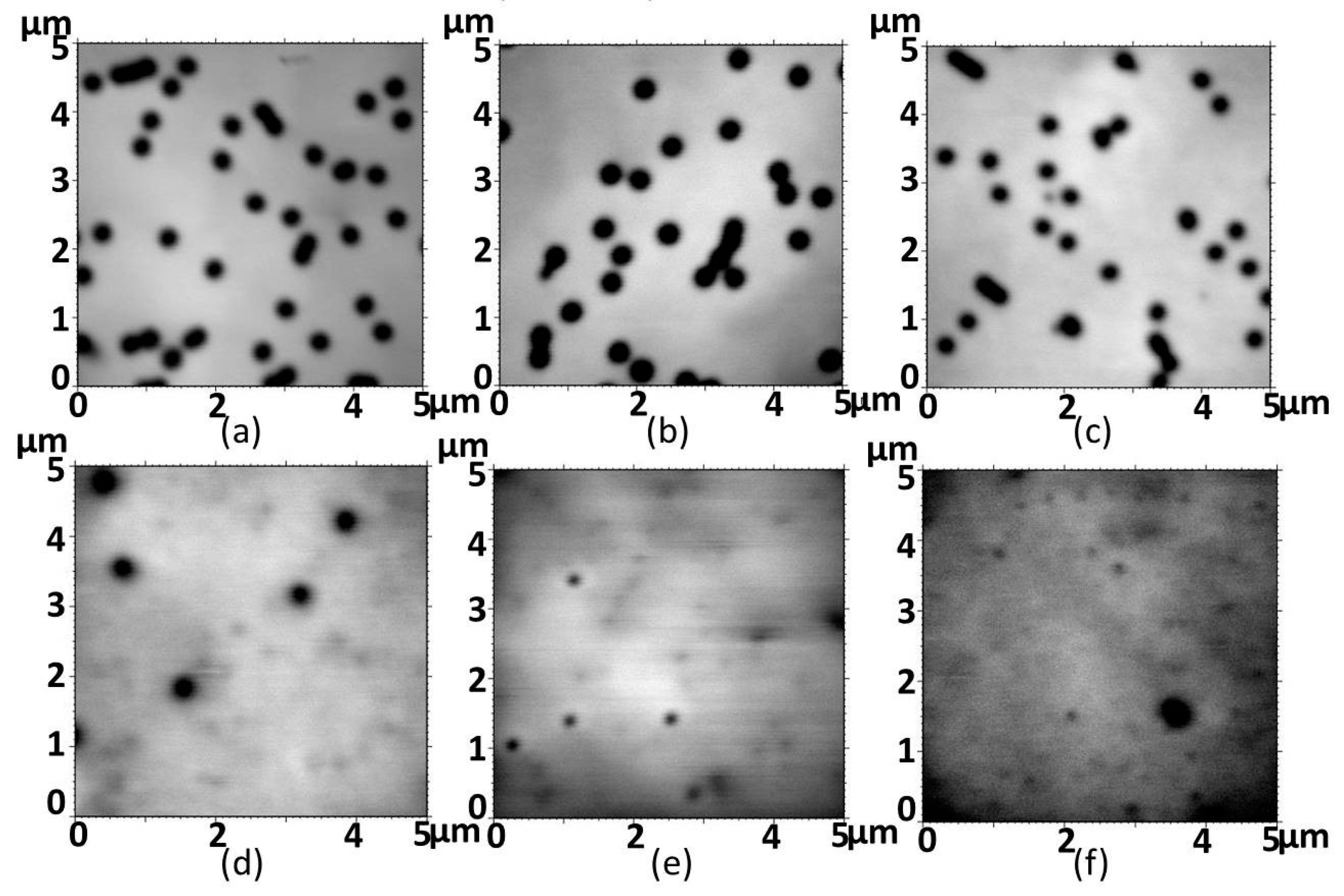
3.1. LED Structure and TEM Images

Figure 1c presents the TEM image of the V-pits of sample A obtained at a low growth temperature of prestrained layers and the V-pit formed during the initial growth stage of prestrained layers along with a TD. The diameter of the V-pits in sample A was approximately 280 nm. Figure 1d presents the TEM image of the V-pits of sample D obtained at a high growth temperature of prestrained layers. In sample D, only small V-pits were obtained near the surface region, and TDs acted as nonradiative recombination centers when they passed through MQWs. This result may have been caused by prestrained layers grown at a lower temperature and higher indium composition, which can lead to V-shaped pit formation from prestrained layers that helped suppress the TD effect. However, when the growth temperature of prestrained layers increased, the reduced indium composition could not facilitate V-shaped pit formation and slowed TDs to directly pass through MQWs (Figure 1d), which can lead to serious nonradiative recombination [32,41].

3.2. CL Monochromatic Analysis

Figure 2a–c present the CL monochromatic images at wavelength of 440 nm and temperature of 300 K of the LED surfaces obtained at a low growth temperature of prestrained layers at 800 °C with 2-μm-thick, 4-μm-thick, and 6-μm-thick n-type-GaN layers, respectively. The V-shaped pit densities of samples A, B, and C were 1.6, 1.24, and 1.12 pits/μm2, respectively. Because the low growth temperature of prestrained layers led to V-shaped pit formation at the initial stage of prestrained layers, V-shaped pits of the larger size of 280 nm were obtained. In addition, the density of V-pits decreased with the increase in the thickness of GaN layers [42]. Because TD could trigger the nucleation of V-shaped pits, the low density of V-shaped pits may have been caused by the low density of TD when the GaN thickness increased. Figure 2d–f present the CL monochromatic images of LEDs obtained at a high growth temperature of prestrained layers at 900 °C and 2-μm-thick, 4-μm-thick, and 6-μm-thick n-type GaN layers, respectively, and the V-shaped pits densities for these LEDs were 0.2, 0.16, and 0.04 pits/μm2, respectively. Few V-shaped pits were formed, and some TDs may have directly passed through the surface or transformed into small V-pits near the surface. Thus, only a few dark spots and many black points are present in Figure 2d–f. The black points caused by TD may have become nonradiative recombination centers and seriously degraded the LED performance [27]. In short, lower prestrained layers growth temperature led to bigger and more V-pits formed. Moreover, thicker nGaN thickness caused reduction of V-pit density.

3.3. Depth-Resolved Confocal Raman Spectroscopy Analysis

To prove a strain relaxation situation, depth-resolved confocal Raman spectroscopy was employed. Figure 3a presents the E2high Raman peaks of all six samples, and the compressive strain status for these E2high Raman peaks appeared at approximately 569.4 cm−1 and that for the E2high Raman peak of unstrained thin film GaN appeared at 568.15 cm−1 [39], so all the six samples suffered about 0.4 GPa of compressive strain. Figure 3b,c illustrates Raman peak shifts in the GaN E2high phonon modes of samples A/B/C (large V-shaped pits) and samples D/E/F (small V-shaped pits) plotted as a function of the depth of the LED structure from the surface (0 μm) toward the substrate. For these six samples, the compressive strain gradually relaxed toward the sample surface from about 0.53 GPa to 0.4 GPa. Most samples presented in Figure 3b (large V-shaped pits) exhibited lower surface strain around 0.1 GPa (0.3 cm−1 of Raman shift) than the samples presented in Figure 3c (small V-shaped pits) did. Figure 3b,c indicates that larger V-shaped pits [28] and thicker GaN led to lower surface strain. As a result, the LED structure with larger V-pits held lower compressive strain.

3.4. CL Spectra and Spatial Distribution

Figure 4a,b presents the CL spectra of samples A/B/C and D/E/F, respectively, wherein two main peaks can be observed. Peaks obtained between 440 and 470 nm were MQWs signals for the 25% indium composition of InGaN well layers. Peaks obtained near 400 nm were the signals of prestrained layers because the indium composition in prestrained InGaN layers was approximately 12%. Moreover, the prestrained layer peaks of samples A/B/C (Figure 4a) were relatively higher than MQW peaks because the emission of prestrained layers could be emitted from large V-shaped pits and the V-shaped pits originated from initial prestrained layers (Figure 1c). In addition, the area of prestrained layers without V-pits was larger than the area of MQWs without V-pits, which could have contributed to the relatively higher peak intensity of prestrained layers. By contrast, all the prestrained layer peaks of samples D/E/F (Figure 4b) were lower than the MQWs peaks of samples D/E/F because the emission of the prestrained layers of samples D/E/F could not be effectively emitted and was absorbed by MQWs. By comparing the intensity ratio between prestrained layer and MQW peaks, we determined whether V-shaped pits were properly formed, and strains were carefully relaxed. Consequently, we established a useful guide to determine the proper growth of prestrained layers.
Based on the aforementioned observation, another remarkable phenomenon was observed during the CL mapping of samples A/B/C (large V-shaped pits) at 10 K. Figure 4c,d illustrates the spatial distribution of CL spectral bands of sample A at 386 and 435 nm, respectively. V-pit locations appeared bright at 386 nm (Figure 4c) (prestrained layers signal) and dark at 435 nm (MQWs signal) (Figure 4d), which suggested that the emission of prestrained layers could be effectively emitted from V-shaped pits, but it could be absorbed by MQW layers. Consequently, brighter light was detected for prestrained layers in V-pit locations than that for plane areas. Thus, V-pit positions were brighter in Figure 4c. At 435 nm, the signals of MQWs exhibited higher emission intensity in plane areas than in V-pit locations (Figure 4d) because the carriers of MQWs in V-shaped pits were trapped by TD, resulting in low emission intensity and dark spots in V-pits.
Figure 4e,f illustrates the spatial distribution of CL spectral bands of sample D at 389 and 438 nm, respectively. Figure 4e illustrates some dark spots of dislocations in prestrained layers; however, few of them can be observed in Figure 4f. This finding was attributed to the formation of fewer V-pits and a poor strain relaxation at the higher growth temperature of prestrained layers. The substandard crystal quality of prestrained layers and MQWs caused by the passing of TDs could lead to the nonradiative recombination of significant carriers near dislocations and dark spots in the CL results of sample D.

3.5. PL Measurement and IQE Analysis

Figure 5a,b presents the PL spectra of samples A/B/C and D/E/F, respectively. The PL intensities of samples A/B/C with large V-pits were higher than those of samples D/E/F with small V-pits. This result strongly agreed with the CL measurement. The PL intensities of sample A and C were the highest and lowest (Figure 5a), respectively, possibly because of the light absorption of thick n-type GaN layers in sample C. However, the PL intensity of sample F with the thickest n-type GaN was the highest (Figure 5b). Small V-pits cannot suppress the lateral diffusion of excited carriers into TDs; however, thick n-type GaN layers not only reduced the TD density [39] but also improved the radiative recombination efficiency, which can compensate the absorption loss in thick n-type GaN layers. Therefore, V-shaped pits initiated at prestrained layers were more crucial than the strain reduction provided by the thick-n-GaN layer.
The sample IQE was measured using power-dependent PL at 12 and 300 K. The data of analyzed quantum efficiency were normalized by defining the maximum IQE value as 100% at 12 K for all samples, and the peak values at 300 K were defined as the room temperature IQE values (Figure 5c,d). With an increase in the pumping power, the point defects were progressively compensated by the injected carriers, leading to an increasing trend of the IQE value. The average value of the best IQE of all samples presented in Figure 5c (samples A/B/C) was more satisfactory than that presented in Figure 5d (samples D/E/F), which strongly agrees with the results of PL intensity.
Sample A exhibited the highest IQE of 93%, and IQE values of sample B and C were approximately 80% (Figure 5c). By contrast, samples D/E/F exhibited the opposite trend, and sample F exhibited the highest IQE of 87% (Figure 5d). The IQE variation strongly agreed with the PL intensity variation (Figure 5a,b). The IQE variation was explained by interaction among V-shaped pits, TDs, and the absorption of n-GaN layers. Briefly summarized, either larger V-pits or thicker nGaN layer could lead to good IQE, but only with a suitable combination of these two conditions could the best device performance be achieved.

3.6. Optical and Electrical Properties of LED Chips by EL Measurement

LED chips with a dimension of 533 × 1092 μm2 were fabricated using the six samples. Table 2 presents the average forward voltage (Vf) and output power (Po) of LED chips when the input current density was 60 A/cm2 (corresponding to the input current of 350 mA). The output power exhibited the same trend as PL intensity did (Figure 5a,b). Samples A and D exhibited the highest and lowest output power, respectively, of 704 and 551 mW, respectively. This finding indicated that GaN LEDs with optimized V-shaped pits under the proper growth condition of prestrained layers and less light absorption layers would provide a high-output power emission. The Vf of samples A/B/C with large V-pits was lower than that of samples D/E/F with small V-pits because large V-pits facilitated a conducting path for carrier injection to MQWs [43]. In addition, samples with thicker n-type GaN layers exhibited lower Vf because of the lower resistance in the thick n-type GaN layer.

4. Conclusions

Strain relaxation and V-shaped pit formation in InGaN MQWs were controlled through the growth temperature of prestrained layers. Lower growth temperature of prestrained layers effectively provided more satisfactory strain relaxation and larger V-shaped pits. The CL measurement results indicated that the peak intensity of prestrained layers and MQWs can be used for determining the strain relaxation level and the original position of V-shaped pits. Furthermore, the results of depth-resolved Raman measurement revealed that less strain can be achieved in thick n-type GaN layers. However, thick n-GaN layers resulted in relatively high optical absorption loss, limiting LED performance. The results indicated that the samples with large V-pits exhibited more satisfactory light output power than did the samples with small V-pits, and the highest power of 704 mW was obtained using the thinnest n-type GaN layer and lower prestrained layer growth temperature (leading to large V-pits). This systematic study provides useful guidelines and a measurement procedure to design LED structures with a suitable combination of excellent strain release from prestrained layers and n-type GaN thickness to obtain high-performance LEDs.

Author Contributions

Conceptualization, T.-C.L. and S.-W.C.; methodology, T.-C.L.; formal analysis, C.-J.C.; investigation, S.-W.C.; writing—original draft preparation, S.-W.C.; writing—review and editing, T.-C.L.; visualization, C.-J.C.; supervision, T.-C.L.; project administration, S.-W.C.; All authors have read and agreed to the published version of the manuscript.

Funding

This research received no external funding.

Acknowledgments

The authors acknowledge Crux Ou and Kirin Lee of Epistar Corporation for their technical support. This work was partially supported by the Research Team of Photonic Technologies and Intelligent Systems from NCTU within the framework of the Higher Education Sprout Project by the Ministry of Education (MOE), Taiwan, and partially by the Ministry of Science and Technology, Taiwan under Contract Numbers MOST 106-2221-E-009-112MY3, 107-2627-E-00 -001, and 108-2119-M-009-003.

Conflicts of Interest

The authors declare no conflict of interest.

References

  1. Ponce, F.; Bour, D. Nitride-based semiconductors for blue and green light-emitting devices. Nature 1997, 386, 351. [Google Scholar] [CrossRef]
  2. Nakamura, S. The roles of structural imperfections in InGaN-based blue light-emitting diodes and laser diodes. Science 1998, 281, 956–961. [Google Scholar] [CrossRef] [PubMed] [Green Version]
  3. Orton, J.; Foxon, C. Group III nitride semiconductors for short wavelength light-emitting devices. Rep. Prog. Phys. 1998, 61, 1. [Google Scholar] [CrossRef]
  4. Ryu, H.; Ha, K.; Lee, S.; Jang, T.; Son, J.; Paek, H.; Sung, Y.; Kim, H.; Kim, K.; Nam, O. High-performance blue InGaN laser diodes with single-quantum-well active layers. IEEE Photonics Technol. Lett. 2007, 19, 1717–1719. [Google Scholar] [CrossRef]
  5. Yoshida, S. Improvements on the electrical and luminescent properties of reactive molecular beam epitaxially grown GaN films by using AlN-coated sapphire substrates. Appl. Phys. Lett. 1983, 42, 427. [Google Scholar] [CrossRef]
  6. Wu, X.H.; Fini, P.; Tarsa, E.J.; Heying, B.; Keller, S.; Mishra, U.K.; DenBaars, S.P.; Speck, J.S. Dislocation generation in GaN heteroepitaxy. J. Cryst. Growth 1998, 189–190, 231–243. [Google Scholar] [CrossRef]
  7. Wu, J.J.; Wang, K.; Yu, T.J.; Zhang, G.Y. GaN substrate and GaN homo-epitaxy for LEDs: Progress and challenges. Chin. Phys. B 2015, 24, 068106. [Google Scholar] [CrossRef]
  8. Ponce, F.; Major, J., Jr.; Plano, W.; Welch, D. Crystalline structure of AlGaN epitaxy on sapphire using AlN buffer layers. Appl. Phys. Lett. 1994, 65, 2302–2304. [Google Scholar] [CrossRef]
  9. Usui, A.; Sunakawa, H.; Sakai, A. Thick GaN epitaxial growth with low dislocation density by hydride vapor phase epitaxy. Jpn. J. Appl. Phys. 1997, 36, L899. [Google Scholar] [CrossRef] [Green Version]
  10. Sasaoka, C.; Sunakawa, H.; Kimura, A.; Nido, M.; Usui, A.; Sakai, A. High-quality InGaN MQW on low-dislocation-density GaN substrate grown by hydride vapor-phase epitaxy. J. Cryst. Growth 1998, 189–190, 61–66. [Google Scholar] [CrossRef]
  11. Lester, S.D.; Ponce, F.A.; Craford, M.G.; Steigerwald, D.A. High dislocation densities in high efficiency GaN-based light-emitting diodes. Appl. Phys. Lett. 1995, 66, 1249. [Google Scholar] [CrossRef]
  12. Sugahara, T.; Sato, H.; Hao, M.; Naoi, Y.; Kurai, S.; Tottori, S.; Yamashita, K.; Nishino, K.; Romano, L.T.; Sakai, S. Direct evidence that dislocations are non-radiative recombination centers in GaN. Jpn. J. Appl. Phys. 1998, 37, L398. [Google Scholar] [CrossRef]
  13. Dai, Q.; Schubert, M.F.; Kim, M.H.; Kim, J.K.; Schubert, E.F.; Koleske, D.D.; Crawford, M.H.; Lee, S.R.; Fischer, A.J.; Thaler, G.; et al. Internal quantum efficiency and nonradiative recombination coefficient of GaInN/GaN multiple quantum wells with different dislocation densities. Appl. Phys. Lett. 2009, 94, 111109. [Google Scholar] [CrossRef] [Green Version]
  14. Petroff, P.; Logan, R.; Savage, A. Nonradiative recombination at dislocations in III–V compound semiconductors. J. Microsc. 1980, 118, 255–261. [Google Scholar] [CrossRef]
  15. Sugahara, T.; Hao, M.; Wang, T.; Nakagawa, D.; Naoi, Y.; Nishino, K.; Sakai, S. Role of dislocation in InGaN phase separation. Jpn. J. Appl. Phys. 1998, 37, L1195. [Google Scholar] [CrossRef]
  16. Schubert, E.F.; Kim, J.K. Solid-state light sources getting smart. Science 2005, 308, 1274–1278. [Google Scholar] [CrossRef]
  17. Krames, M.; Bhat, J.; Collins, D.; Gardner, N.; Götz, W.; Lowery, C.; Ludowise, M.; Martin, P.; Mueller, G.; Mueller-Mach, R. High-Power III-Nitride Emitters for Solid-State Lighting. Physica Status Solidi (A) 2002, 192, 237–245. [Google Scholar] [CrossRef]
  18. Nizamoglu, S.; Demir, H.V. Hybrid white light sources based on layer-by-layer assembly of nanocrystals on near-UV emitting diodes. Nanotechnology 2007, 18, 405702. [Google Scholar] [CrossRef]
  19. Fang, Z.; Lin, D.; Kang, J.; Kong, J.; Shen, W. Interface modification of the InGaN/GaN quantum wells: The strain pre-relief effect. Nanotechnology 2009, 20, 235401. [Google Scholar] [CrossRef]
  20. Chen, Y.; Takeuchi, T.; Amano, H.; Akasaki, I.; Yamada, N.; Kaneko, Y.; Wang, S.Y. Pit formation in GaInN quantum wells. Appl. Phys. Lett. 1998, 72, 710. [Google Scholar] [CrossRef]
  21. Shiojiri, M.; Chuo, C.C.; Hsu, J.T.; Yang, J.R.; Saijo, H. Structure and formation mechanism of V defects in multiple InGaN/GaN quantum well layers. J. Appl. Phys. 2006, 99, 073505. [Google Scholar] [CrossRef]
  22. Wu, X.H.; Elsass, C.R.; Abare, A.; Mack, M.; Keller, S.; Petroff, P.M.; DenBaars, S.P.; Speck, J.S. Structural origin of V-defects and correlation with localized excitonic centers in InGaN/GaN multiple quantum wells. Appl. Phys. Lett. 1998, 72, 692–694. [Google Scholar] [CrossRef]
  23. Kim, J.; Kim, J.; Tak, Y.; Chae, S.; Kim, J.-Y.; Park, Y. Effect of V-shaped pit size on the reverse leakage current of InGaN/GaN light-emitting diodes. IEEE Electron Device Lett. 2013, 34, 1409–1411. [Google Scholar] [CrossRef]
  24. Hangleiter, A.; Hitzel, F.; Netzel, C.; Fuhrmann, D.; Rossow, U.; Ade, G.; Hinze, P. Suppression of nonradiative recombination by V-shaped pits in GaInN/GaN quantum wells produces a large increase in the light emission efficiency. Phys. Rev. Lett. 2005, 95, 127402. [Google Scholar] [CrossRef] [PubMed] [Green Version]
  25. Kurai, S.; Higaki, S.; Imura, N.; Okawa, K.; Makio, R.; Okada, N.; Tadatomo, K.; Yamada, Y. Potential Barrier formed around dislocations in InGaN quantum well structures by spot cathodoluminescence measurements. Physica Status Solidi (B) 2018, 255, 1700358. [Google Scholar] [CrossRef]
  26. Wang, C.H.; Chen, J.R.; Chiu, C.H.; Kuo, H.C.; Li, Y.L.; Lu, T.C.; Wang, S.C. Temperature-Dependent Electroluminescence Efficiency in Blue InGaN–GaN Light-Emitting Diodes With Different Well Widths. IEEE Photonics Technol. Lett. 2010, 22, 236–238. [Google Scholar] [CrossRef]
  27. Kim, J.; Cho, Y.-H.; Ko, D.-S.; Li, X.-S.; Won, J.-Y.; Lee, E.; Park, S.-H.; Kim, J.-Y.; Kim, S. Influence of V-pits on the efficiency droop in InGaN/GaN quantum wells. Opt. Express 2014, 22, A857–A866. [Google Scholar] [CrossRef]
  28. Okada, N.; Kashihara, H.; Sugimoto, K.; Yamada, Y.; Tadatomo, K. Controlling potential barrier height by changing V-shaped pit size and the effect on optical and electrical properties for InGaN/GaN based light-emitting diodes. J. Appl. Phys. 2015, 117, 025708. [Google Scholar] [CrossRef]
  29. Zhou, S.; Liu, X. Effect of V-pits embedded InGaN/GaN superlattices on optical and electrical properties of GaN-based green light-emitting diodes. Physica Status Solidi (A) 2017, 214, 1600782. [Google Scholar] [CrossRef]
  30. Wu, X.; Liu, J.; Jiang, F. Hole injection from the sidewall of V-shaped pits into c-plane multiple quantum wells in InGaN light emitting diodes. J. Appl. Phys. 2015, 118, 164504. [Google Scholar] [CrossRef]
  31. Liu, Y.-J.; Tsai, T.-Y.; Yen, C.-H.; Chen, L.-Y.; Tsai, T.-H.; Liu, W.-C. Characteristics of a GaN-based light-emitting diode with an inserted p-GaN/i-InGaN superlattice structure. IEEE J. Quantum Electron. 2010, 46, 492–498. [Google Scholar] [CrossRef]
  32. Armstrong, A.M.; Bryant, B.N.; Crawford, M.H.; Koleske, D.D.; Lee, S.R.; Wierer, J.J., Jr. Defect-reduction mechanism for improving radiative efficiency in InGaN/GaN light-emitting diodes using InGaN underlayers. J. Appl. Phys. 2015, 117, 134501. [Google Scholar] [CrossRef]
  33. Lee, K.; Lee, C.-R.; Lee, J.H.; Chung, T.-H.; Ryu, M.-Y.; Jeong, K.-U.; Leem, J.-Y.; Kim, J.S. Influences of Si-doped graded short-period superlattice on green InGaN/GaN light-emitting diodes. Opt. Express 2016, 24, 7743–7751. [Google Scholar] [CrossRef] [PubMed]
  34. Lee, K.; Lee, C.-R.; Chung, T.-H.; Park, J.; Leem, J.-Y.; Jeong, K.-U.; Kim, J.S. Influences of graded superlattice on the electrostatic discharge characteristics of green InGaN/GaN light-emitting diodes. J. Cryst. Growth 2017, 464, 138–142. [Google Scholar] [CrossRef]
  35. Chen, S.-W.; Li, H.; Lu, T.-C. Improved performance of GaN based light emitting diodes with ex-situ sputtered AlN nucleation layers. AIP Adv. 2016, 6, 045311. [Google Scholar] [CrossRef]
  36. Davydov, V.Y.; Kitaev, Y.E.; Goncharuk, I.N.; Smirnov, A.N.; Graul, J.; Semchinova, O.; Uffmann, D.; Smirnov, M.B.; Mirgorodsky, A.P.; Evarestov, R.A. Phonon dispersion and Raman scattering in hexagonal GaN and AlN. Phys. Rev. B 1998, 58, 12899–12907. [Google Scholar] [CrossRef] [Green Version]
  37. Harima, H. Properties of GaN and related compounds studied by means of Raman scattering. J. Phys. Condens. Matter 2002, 14, R967–R993. [Google Scholar] [CrossRef]
  38. Kisielowski, C.; Krüger, J.; Ruvimov, S.; Suski, T.; Ager, J.W.; Jones, E.; Liliental-Weber, Z.; Rubin, M.; Weber, E.R.; Bremser, M.D.; et al. Strain-related phenomena in GaN thin films. Phys. Rev. B 1996, 54, 17745–17753. [Google Scholar] [CrossRef] [Green Version]
  39. Choi, S.; Heller, E.; Dorsey, D.; Vetury, R.; Graham, S. Analysis of the residual stress distribution in AlGaN/GaN high electron mobility transistors. J. Appl. Phys. 2013, 113, 093510. [Google Scholar] [CrossRef]
  40. Wagner, J.-M.; Bechstedt, F. Properties of strained wurtzite GaN and AlN: Ab initio studies. Phys. Rev. B 2002, 66, 115202. [Google Scholar] [CrossRef]
  41. Kumano, H.; Hoshi, K.-I.; Tanaka, S.; Suemune, I.; Shen, X.-Q.; Riblet, P.; Ramvall, P.; Aoyagi, Y. Effect of indium doping on the transient optical properties of GaN films. Appl. Phys. Lett. 1999, 75, 2879–2881. [Google Scholar] [CrossRef] [Green Version]
  42. Jasinski, J.; Liliental-Weber, Z. Extended defects and polarity of hydride vapor phase epitaxy GaN. J. Electron. Mater. 2002, 31, 429–436. [Google Scholar] [CrossRef]
  43. Li, C.-K.; Wu, C.-K.; Hsu, C.-C.; Lu, L.-S.; Li, H.; Lu, T.-C.; Wu, Y.-R. 3D numerical modeling of the carrier transport and radiative efficiency for InGaN/GaN light emitting diodes with V-shaped pits. AIP Adv. 2016, 6, 055208. [Google Scholar] [CrossRef] [Green Version]
Figure 1. LED structures with (a) large V-pits originated from prestrained layers and (b) small V-pits originated after electron blocking layer (EBL). The black lines illustrate the propagation of threading dislocations. TEM images of LED samples with (c) large V-pits and (d) small V-pits (identified using red arrows).
Crystals 10 00311 g001
Figure 2. Cathodoluminescence (CL) monochromatic images of LED surfaces. Large V-pit samples with (a) 2-μm-thick, (b) 4-μm-thick, and (c) 6-μm-thick n-type GaN layers, respectively. Small V-pits samples with (d) 2-μm-thick, (e) 4-μm-thick, and (f) 6-μm-thick n-type GaN layers, respectively.
Crystals 10 00311 g002
Figure 3. (a) Zoomed-in view of the E2high Raman peaks of all samples. Raman peak shifts of the GaN E2high phonon modes of (b) samples A/B/C (with large V-pits, typically 569.2–569.4 cm−1 at surface) and (c) D/E/F (with small V-pits, typically 569.4–569.8 cm−1 at surface) plotted as a function of the depth of the LED structure from the surface (0 μm) toward substrate.
Crystals 10 00311 g003
Figure 4. CL spectra of samples (a) A/B/C and (b) D/E/F measured at 10 K. Spatial distribution of CL spectral bands of sample A at (c) 386 and (d) 435 nm. Spatial distribution of CL spectral bands of sample D at (e) 389 and (f) 438 nm.
Crystals 10 00311 g004
Figure 5. PL spectra of samples (a) A/B/C and (b) D/E/F. Normalized internal quantum efficiency (IQE) values of MQWs as a function of pumping power at 12 K and 300 K of samples (c) A/B/C and (d) D/E/F.
Crystals 10 00311 g005
Table 1. Samples A–F with their thickness of nGaN and growth temperature of prestrained layers.
SampleThickness of nGaN (μm)Growth Temperature of Prestrained Layers (°C)
A2800
B4800
C6800
D2900
E4900
F6900
Table 2. Forward voltage (Vf) and output power (Po) at injection current of 350 mA for all samples with a chip size of 533 × 1092 μm2.
SampleVf (V)Po (mW)
A3.39704
B3.32701
C3.31680
D5.05551
E3.98560
F3.42633

