
Highly Conductive n-Al0.65Ga0.35N Grown by MOCVD Using Low V/III Ratio
by
Christian J. Zollner
1,2,*, 
Yifan Yao
1,2,
Michael Wang
1,2,
Feng Wu
1,2,
Michael Iza
1,2,
James S. Speck
1,2,
Steven P. DenBaars
1,2,3 and
Shuji Nakamura
1,2,3 1
Materials Department, University of California Santa Barbara (UCSB), Santa Barbara, CA 93106, USA
2
Solid State Lighting and Energy Electronics Center, UCSB, Santa Barbara, CA 93106, USA
3
Department of Electrical and Computer Engineering, UCSB, Santa Barbara, CA 93106, USA
*
Author to whom correspondence should be addressed.
Crystals 2021, 11(8), 1006; https://doi.org/10.3390/cryst11081006
Submission received: 13 August 2021
/
Revised: 18 August 2021
/
Accepted: 19 August 2021
/
Published: 23 August 2021
(This article belongs to the Section Inorganic Crystalline Materials)
Abstract
:Highly conductive silicon-doped AlGaN and ohmic contacts are needed for deep-UV LEDs and ultrawide bandgap electronics. We demonstrate improved n-Al0.65Ga0.35N films grown by metal–organic chemical vapor deposition (MOCVD) on sapphire substrates using a low V/III ratio (V/III = 10). A reduced V/III ratio improves repeatability and uniformity by allowing a wider range of silicon precursor flow conditions. AlxGa1−xN:Si with x > 0.5 typically has an electron concentration vs. silicon concentration trend that peaks at a particular “knee” value before dropping sharply as [Si] continues to increase (self-compensation). The Al0.65Ga0.35N:Si grown under the lowest V/III conditions in this study does not show the typical knee behavior, and instead, it has a flat electron concentration trend for [Si] > 3 × 1019 cm−3. Resistivities as low as 4 mΩ-cm were achieved, with corresponding electron mobility of 40 cm2/Vs. AFM and TEM confirm that surface morphology and dislocation density are not degraded by these growth conditions. Furthermore, we report vanadium-based ohmic contacts with a resistivity of 7 × 10⁻⁵ Ω-cm2 to AlGaN films grown using a low V/III ratio. Lastly, we use these highly conductive silicon-doped layers to demonstrate a 284 nm UV LED with an operating voltage of 7.99 V at 20 A/cm2, with peak EQE and WPE of 3.5% and 2.7%, respectively.
1. Introduction
Ultrawide bandgap semiconductors are one of the fastest growing areas of semiconductor research and device commercialization. Applications of ultrawide bandgap materials include high voltage, high temperature, radiation-hard electronic devices, radio-frequency devices and integrated circuits, gas-phase chemical detection, and deep ultraviolet (UV) optoelectronics [1,2]. The most well understood and commercially produced ultrawide bandgap material is AlxGa1−xN, which can be grown epitaxially with high quality on commercially available substrates and has a tunable bandgap between 6.2 eV (AlN) and 3.4 eV (GaN). This allows the fabrication of LEDs and laser diodes with emission wavelengths spanning the UV-A, UV-B, and UV-C bands.
High-voltage electronics based on AlGaN have already demonstrated outstanding critical breakdown field values, and they are mostly limited by series resistance and mobility constraints due to high contact resistance and bulk n-type resistivity of AlGaN with an Al molar fraction above 50%. The cost per watt of germicidal ultraviolet (GUV) LEDs has decreased by a factor of 500 in the past decade due to several breakthroughs in AlGaN material quality, electrical conductivity, optical quality, and device design, but it is still 100 times higher than the current incumbent GUV technology: Hg vapor lamps. To enable increased GUV LED adoption, additional advances are needed, especially regarding optical transparency (light extraction efficiency) and driving voltage (electrical or voltage efficiency).
One significant contribution to GUV LED driving voltage comes from the n-side series resistance. This includes the ohmic contact and n-AlxGa1−xN current spreading layer (in which the Al-molar fraction, x, must be greater than 65% for GUV-transparency), wherein electrical current spreads over tens or hundreds of microns to the center of the LED mesa. More importantly, high n-AlGaN sheet resistance values result in current crowding, which occurs when the lateral resistance is high compared to the vertical (p-side) resistance. The characteristic current spreading length and series resistance are proportional to Rsh−1/2 and Rsh, respectively (wherein Rsh is the sheet resistance of the n-AlGaN layer, Rsh = ρ/t, where ρ is the electrical resistivity and t is the n-AlGaN thickness). We estimate that a sheet resistance of no more than 100 Ω/□ is needed to enable uniform, low-voltage-drop current injection (without n-side current crowding) in UV LEDs with mesa sizes on the order of 0.1 mm2 [3]. Bulk n-type resistivity can be written as ρ−1 = enμ, where e is the electron charge, n is the electron concentration, and μ is the electron mobility. Thus, the sheet resistance can be reduced by (1) increasing the n-AlGaN thickness, (2) increasing the electron concentration, and (3) increasing the electron mobility.
There are some reports of deep UV optoelectronic devices with very thick n-AlGaN [4,5,6], showing that it is feasible to produce high-WPE devices using this approach, but there are some risks to growing n-AlGaN to thicknesses greater than 1 μm. First, any optical absorption will be increased with layer thickness. Second, dislocation inclination in epitaxial Si-doped AlGaN is known to lead to residual tension causing wafer bow or cracking [7,8,9], which are detrimental to device operation. Third, if growth conditions are not precisely optimized, surface morphology may worsen with increasing thickness, degrading active region performance. Thus, there is a benefit to decreasing n-AlGaN resistivity rather than increasing the thickness of the layer greatly.
Electron mobility in highly conductive n-AlGaN is lower than in GaN: it is typically between 5 and 100 cm2/Vs in material used for GUV LEDs. As a result, electron concentrations (and thus, silicon concentrations) must be above 1019 cm−3 for low resistivity. Arbitrarily high [Si] can be achieved by metal–organic chemical vapor deposition (MOCVD), but above some threshold [Si], additional impurity incorporation ceases to provide additional free electrons. For very high [Si], there is usually an inversion of the relationship between [Si] and n, meaning that the additional Si atoms above this threshold either cease to act as shallow donors or are compensated by acceptor defects [10,11,12,13]. This threshold effect is referred to in the literature as self-compensation or knee behavior. The threshold or knee [Si] value above which self-compensation begins can be altered via tuning of the growth conditions. Therefore, methods for MOCVD growth of highly conductive AlGaN depend on the development of growth conditions that maximize [Si] incorporation while remaining below the self-compensation threshold.
We have recently demonstrated that the self-compensation behavior of Al0.65Ga0.35N has a strong dependence on growth temperature and growth rate [14], which is in agreement with recent theoretical [15] and experimental reports [12,16,17,18]. In this work, we show that the V/III ratio during MOCVD growth has a similarly important effect. In particular, we find that growth at low V/III ratios below 100 enables electron concentrations up to 3 × 1019 cm−3, without any evidence of knee behavior. At more conventional V/III ratios above 100, we find a typical self-compensation behavior with sensitive dependence of electron concentration on silicon precursor flow. Next, we develop low-contact-resistivity ohmic contacts using a vanadium-based multilayer stack and rapid thermal annealing, and we demonstrate a UV LED grown on this n-AlGaN layer with an emission wavelength of 284 nm and a voltage efficiency above 50% at 20 A/cm2.
2. Materials and Methods
Nitride films were grown by MOCVD with trimethylaluminum (TMA) and trimethylgallium (TMG) group III precursors, disilane (Si2H6) for n-type doping, and NH3, under a hydrogen carrier gas. Trimethylindium (TMI) was also used as a surfactant to improve surface morphology and conductivity [14]. AlN/sapphire templates were supplied by Enkris Semi. Inc. and Kyma Tech. Inc. First, 150 nm thick AlN buffer layers were deposited, followed by 50 nm thick undoped Al0.85Ga0.15N interlayers. Next, Si-doped Al0.65Ga0.35N films up to 700 nm thick were grown using a thermocouple temperature of 1200 °C and reactor pressure of 20 kPa. Three different NH3 flow rates of 4 sccm, 20 sccm, and 40 sccm were used, corresponding to molar V/III ratios of 10, 119, and 277, respectively. Reactor pressures and V/III ratios are not universally reported in the high-Al AlGaN literature; based on the limited number of reports, we expect that these are among the highest pressure and lowest V/III ratios reported for highly conductive AlxGa1−xN with x > 0.5.
Samples were fabricated into Van der Pauw patterns for Hall measurements and circular transmission line method (CTLM) structures for characterizing contact resistivity. Dry etching was performed using SiCl4-based reactive ion etching, and contacts were deposited using electron beam deposition and then annealed using a rapid thermal annealing (RTA) system under N2 ambient at temperatures between 700 and 940 °C for 30 seconds. The UV LED sample was further processed using a semi-transparent thin metal contact (2 nm Ni/3 nm Pt) and thick p-side contact pad (10 nm Ti/300 nm Au).
Hall measurements were conducted using both annealed V-based contacts and soldered indium contacts. Lithographically defined Van der Pauw structures enable precise, local measurements of carrier concentration and mobility, whereas indium contacts provide approximate, average values across the entire epitaxy surface. Magnetic fields of ±0.2 T, ±0.4 T, and ±0.6 T were used with currents up to 0.1 mA. Good agreement (<5% variation) was found between both contact types and all magnetic fields, indicating good epitaxial uniformity.
Contact resistivity was measured by the CTLM method [19] with currents up to 500 mA, constant inner pad radius, L, and varying gap distance, d. The contact resistivity, Rc, can be calculated from total resistance values, R, using the full CTLM solution:
via
where LT is the transfer length and Rsh is the sheet resistance of the film. I0, I1, K0, and K1 are the hyperbolic Bessel function solutions of the first kind and second kind.
Atomic force microscopy (AFM) was carried out using an Asylum MFP-3D in AC mode with a high-stiffness cantilever. High-angle annular dark field (HAADF) scanning transmission electron microscopy (STEM) and Energy-Dispersive X-ray Spectroscopy (EDS) mapping were performed with a ThermoFisher Talos G2 200X TEM/STEM (Thermo Scientific, Santa Clara, CA, USA) system operated at 200 kV. The sample for HAADF-STEM and EDS was prepared by the focused ion beam (FIB) technique with an FEI Helios Dualbeam Nanolab 600 instrument (Thermo Scientific, Santa Clara, CA, USA).
The alloy composition and degree of relaxation were confirmed by high resolution X-ray diffraction using the reciprocal space mapping (RSM) technique near the AlGaN and AlN (105) reflections. The incident beam was conditioned using an intensifier and Ge (220) two-bounce nondispersive monochromator, and the diffracted beam was collected using a Rigaku HyPix array detector. RSM data (not shown) indicate a low degree of relaxation for the n-AlGaN layers studied in this report. Dynamic secondary ion mass spectroscopy (using a Cameca IMS 7f auto SIMS, AMETEK, Inc., Berwyn, PA, USA) with a magnetic-sector mass filter was used to measure the concentration of Si and other impurities in AlGaN films. The Cs+ primary beam energy was 15 kV, and measurements were performed using high mass resolution to distinguish between 28Si, N2, and 27Al1H ions.
UV LED characteristics were measured using a Keithley source-meter, 75 mm diameter integrating sphere, and spectrophotometer recently calibrated by Instrument Systems. Calibration was confirmed by comparison with commercially available UV-B and UV-C LEDs. Power and voltage were measured under continuous current-supply conditions, using auto-ranging integration times between 1 and 5 s.
3. Results
We report the effect of the molar ratio of group V (NH3) and group III (TMA and TMG) MOCVD precursors, known as the V/III ratio, on the composition and n-type conductivity of AlxGa1−xN:Si with x = 0.65 ± 0.05. First, the relationship between NH3 flow and molar efficiency for both TMG and TMA precursors was investigated to determine the proper growth conditions for 65% AlGaN with a constant growth rate (GR) around 2 Å/s over a wide range of V/III ratios. It was found that V/III had some effect on GR, such that a decrease of about a factor of one-half in TMA was needed to maintain constant GR and composition at the highest NH3 values. On the other hand, the necessary TMG to maintain 65% composition reduced by nearly an order of magnitude between NH3 flows of 4 sccm and 400 sccm (corresponding to V/III of 10 and 6000, respectively). As NH3 flow was increased further above 400 sccm, the necessary TMG flow increased again. Data for the TMG flow needed to maintain 65% Al are shown in Figure 1.
Next, the effect of disilane flow on Si incorporation was investigated under various V/III conditions. A steady increase in Si incorporation with increasing disilane flow (as shown in Figure 2, with log-linear trendlines to guide the eye) was observed for all growth conditions investigated here. For V/III ratios > 1000, no highly conductive films were observed under these temperature and growth rate conditions. In the three low V/III conditions shown in Figure 2, increasing [Si] > 3 × 1019 cm−3 failed to increase the electron concentration, n, in the material. Instead, the additional silicon either led to a knee behavior (in the V/III = 119 and 277 cases), or to a saturation in electron concentration (in the V/III = 10 case). Additional SIMS data (not shown) confirmed that [C] incorporation was too low to account for the observed compensation, and the threading dislocation density was low enough that compensation by dislocations could be neglected [15]. The lowest achieved resistivity using V/III = 10 was 4 mΩ-cm for 65% Al molar fraction, with samples above 70% Al exhibiting resistivities as low as 9 mΩ-cm. The growth window—i.e., the range of disilane/III molar ratios over which ρ < 10 mΩ-cm was achieved—was 5 × 10⁻⁴ for V/III = 10 but narrowed to <10−4 for V/III > 100.
For V/III ratios > 100, the inversion of the [Si] vs. n relation also corresponds to a sharp reduction in electron mobility from around 40 cm2/Vs to below 10 cm2/Vs. As a result, the window of optimal doping conditions was quite narrow, since both electron concentration and mobility sharply decreased above the self-compensation threshold. In contrast, there was only a very slight reduction in electron mobility at high [Si] levels in the V/III = 10 growths—thus resulting in a wider doping window.
AFM (Figure 3) shows the effect of V/III ratio on surface morphology. The initial MOCVD-grown AlN buffer layer had an atomically flat surface with sub-nanometer RMS roughness and evidence of a smooth step-flow growth mode. AlGaN:Si grown under the lowest V/III conditions had an undulating or hillock morphology, which is atomically flat on a local, sub-μm length scale. Most hillocks appear to be terminated by a small pit, which is indicative of a dislocation-mediated hillock step flow growth mechanism [20,21,22]. A mixture of pits with and without step termination (indicative of screw-component and pure-edge dislocations, respectively) was observed on closer inspection (not shown). For V/III ratios > 100, the width and height of the hillock features increased, leading to a rougher morphology with sharper features more typical of highly Si doped AlGaN [16,23]. RMS roughness values of approximately 4 nm, 5 nm, and 6 nm were calculated for n-AlGaN films grown under V/III = 10, 119, and 277, respectively. Smoother morphology could be achieved by, e.g., increasing growth temperature, increasing V/III, or reducing growth rate, but these changes lead to reduced conductivity [14]. We show below that the morphology for V/III = 10 is sufficiently smooth to enable efficient UV LED operation.
Electron microscopy images of a sample with an undoped interlayer and two thick n-AlGaN layers with different compositions are shown in Figure 4. Cross-sectional TEM confirmed that the growth of AlGaN occurred coherently on the AlN template, and there was no generation of additional dislocations at the AlGaN/AlN interface. TEM-EDS indicated smooth, sharp interfaces between regions of different AlGaN molar composition and spatially uniform compositions. The undulating morphology of the thick AlGaN:Si layer can be observed most clearly in the Ga signal. The interface between the topmost AlGaN layer and the layer below it appears less sharp due to surface roughness.
Using the optimized AlGaN:Si conditions shown in Figure 2, with V/III = 10, we next compared various ohmic contact formation methods to produce low-resistance contacts. It is well known that Ti-based ohmic contacts (such as those used for n-GaN) fail to produce low-resistance ohmic contacts for AlxGa1−xN with x > 0.6. In Figure 5a, we compare the ohmic contact behavior for various Ti- and V-based metal stacks, all annealed at 900 °C. By replacing the Ti contact layer (the first deposited layer) with V, contact resistance is greatly improved [24]. Next, the diffusion barrier layer (third deposited layer) was varied. Replacing the V barrier with a Ni barrier again greatly improved the contact resistance, perhaps because it reduced the intermixing between Au and Al. Increasing the Ni thickness from 20 to 150 nm did not provide any additional benefit. Increasing the Ni thickness further is not advisable due to the high internal stresses present in electron-beam deposited Ni films, which sometimes lead to delamination.
An annealing temperature of 900 °C was found to be optimal for the ohmic contacts investigated in this work, as shown in Figure 5b. Annealing above or below this temperature diminished the ohmic character of the contacts and increased the contact resistivity. The sensitivity of V-based contacts to annealing temperature is a matter of debate, but it may be related to the formation of donor-like nitrogen vacancies near the surface of the semiconductor [25].
Finally, using the most optimized Si:AlGaN films and ohmic contacts, we used the CTLM method to calculate the contact resistance, as detailed in Figure 6. Using Equations (1) and (2), we calculate a contact resistance of 7 × 10⁻⁵ Ω-cm2 and a sheet resistance of 90 Ω/□. This sheet resistance is in good agreement with the sheet resistance determined by the Van der Pauw method, as shown in Figure 2, and it is sufficiently low to prevent current crowding in a UV LED device.
To demonstrate that the conductivity, structural quality, and smoothness of the optimized n-AlGaN layer was sufficient for UV LED operation, a device-active region and hole injection structure as described previously [26] were deposited atop this n-AlGaN layer. This UV LED device was processed and packaged using a novel high-LEE architecture, which will be described in a future communication. Due to the low sheet and contact resistances of the n-side of the device, the LED had an operating voltage below 8 V, which was expected to be mostly limited by the p-side contact. This 284 nm device achieved 2.5 mW of output power with peak EQE and WPE of 3.5% and 2.7%, respectively. The voltage efficiency was 81% at peak WPE and 54% at 20 A/cm2. Voltage, power, and efficiency data are shown in Figure 7. A microscope image taken during an on-wafer device testing (Figure 7b, inset) shows uniform current injection, confirming that the n-AlGaN sheet resistance is sufficiently low to prevent current crowding.
4. Discussion
The knee behavior in silicon-doped AlxGa1−xN with x > 0.6 is well studied and nearly universally observed in heavily Si-doped samples. Some early reports found knee behavior above [Si] ≈2 × 1018 cm−3 (x = 0.6) [27] or as low as 4 × 1017 cm−3 (x = 0.54) [11]. Decreased growth temperature and V/III ratio both lead to less abrupt knee characteristics with higher threshold [Si] values, with recent reports confirming successful [Si] doping above 1019 cm−3 via optimized growth conditions [12,14,15,16,17,18]. Extrinsic impurities can be ruled out as the major compensating defects in heavily doped AlGaN:Si using SIMS [10,11,12,14,27]. Donor compensation in n-AlGaN is most likely due to group-III vacancies (VIII) and perhaps vacancy complexes (VIII-X, e.g., VIII-SiIII). Vacancy concentrations can be quantified in order-of-magnitude terms by positron annihilation spectroscopy (PAS), if certain assumptions are made about the properties of the predicted vacancies and complexes [27,28]. Uedono et al. found a decrease in luminescence lifetimes [27] and increased PAS signature of VIII in AlGaN with increased Si doping, suggesting VIII-SiIII complexes as the likely explanation [11].
We find for the first time that using a V/III ratio < 100 greatly reduces the self-compensation effect, producing an n vs. [Si] vs. relation, which flattens at around n = 3 × 1019 cm−3 rather than decreasing (no knee behavior). By growing with an elevated reactor pressure of 20 kPa (150 Torr), the thermodynamic driving force for AlGaN growth can be increased without the need for an increased V/III ratio [29]. We speculate that the use of elevated reactor pressures enables the growth of AlGaN at very low V/III ratios below 100, which may not be feasible at more typical reactor pressures used for AlGaN (<5 kPa).
There are few reports of the dependence of mobility on silicon concentration in heavily Si-doped n-AlGaN samples [30,31,32]. As shown in Figure 2, the mobility trend appears to correspond qualitatively with the knee behavior in the electron concentration trends. In both the moderate V/III datasets, the onset of knee behavior in electron concentration clearly accompanies a sharp drop in electron mobility. This order-of-magnitude decrease in mobility is attributed to ionized impurity scattering, which is most likely due to the same compensating defects that reduce the electron concentration. In the lowest V/III dataset, there is no drastic drop in electron mobility. This is in good agreement with the trend in electron concentration, which does not suggest there is any significant formation of charged compensating defects above [Si] = 3 × 1019 cm−3. The lack of knee behavior in electron concentration, combined with the more gradual decrease in mobility, leads to a much wider doping window in the lowest V/III condition, improving the repeatability and uniformity of the process.
It is plausible that the excess silicon atoms above ≈3 × 1019 cm−3 in the V/III = 10 case (which do not contribute free electrons) may be incorporating in some neutral defect configuration; this would explain the lack of donor compensation and the much weaker reduction in mobility. Harris et al. have proposed that numerous VIII + nSiIII complexes are stable in n-type AlGaN [28]. Whereas VIII + 1SiIII and VIII + 2SiIII are acceptors in n-type AlGaN, VIII + 3SiIII is most stable in a charge-neutral configuration. It may be the case that the extreme conditions present in the lowest V/III environment with high reactor pressure, TMI surfactant, and high disilane injection promote the formation of VIII + 3SiIII or some other neutral vacancy complex not routinely observed under conventional growth conditions for n-AlGaN (pressures below 5 kPa, V/III > 500, silane precursor, and no TMI surfactant).
To the authors’ knowledge, this is the first report of highly conductive AlxGa1−xN with x > 0.5 using a disilane precursor. It is commonly reported that the pyrolysis of SiH4 is temperature-independent above 750 °C (and, therefore, that there should be no significant advantage to using Si2H6), but this is strictly only true at atmospheric pressure. Under low-pressure conditions such as those used for Al-rich AlGaN MOCVD, there may be some temperature dependence for SiH4 even above 1000 °C [33].
There are many conflicting reports discussing the best metal stack and annealing conditions for V-based ohmic contacts to n-AlGaN [25,34,35,36]. The success of V-based ohmic contacts has historically been explained by the formation of VN, which has the lowest work function (3.5 eV) of any experimentally investigated contact material (for comparison, TaN, WN, MoN, TiN, Ti, and V all have work functions above 4 eV) [37]. On the other hand, Sulmoni et al. [25] have recently reported that little or no VN is formed at good ohmic contacts to n-AlGaN, and rather that a thin AlN layer is formed at the contact interface. Reported V-based contact annealing temperatures usually range between 700 and 900 °C, with higher Al-content alloys requiring higher temperatures. It seems that the optimal metallization and annealing conditions differ depending on the details of the material (alloy composition, surface preparation [24,38], and doping level), and that different metal stacks require different annealing conditions. Therefore, iterative and empirical optimization is needed to achieve good ohmic contacts to n-AlGaN.
Growing under low V/III conditions leads to a hillock morphology that is atomically flat on a local scale, but undulating over micron-length scales. We find that the surface morphology can be restored to an atomically flat step-flow growth mode using a pulsed, high-V/III condition (details will be provided in a future publication). In order to confirm that this hillock morphology does not degrade multi-quantum well-active regions grown above this Si-doped layer, we grew a UV LED structure including an active region, p-AlGaN superlattice [26], and p-GaN contact layer above the Si:AlGaN layer. Our findings show that good EQE and WPE can be achieved using this n-AlGaN growth condition.
5. Conclusions
We report that highly conductive n-type AlGaN alloys with an Al molar fraction above 65% can be produced by MOCVD with V/III ratios < 100. We confirm that self-compensation effects dominate the Si vs. n relation for [Si] > 3 × 1019 cm−3 for moderate V/III ratios > 100, but we do not observe any significant knee behavior for samples grown with V/III = 10. As a result, the range of permissible disilane flow values yielding highly conductive material is much wider at the lowest V/III conditions, enabling more repeatable and uniform growths. We find that the elevated reactor pressure of 20 kPa, use of disilane precursor, and use of TMI indium surfactant-assisted growth enable good material quality, low [C] incorporation, and smooth surface morphology despite the low NH3 flow and reduced growth temperature.
We also find that V-based ohmic contacts to n-AlGaN can be made using optimized metallization and annealing conditions, achieving a contact resistance of 7 × 10⁻⁵ Ω-cm2. With optimized n-AlGaN and ohmic contacts, we achieve a 284 nm UV LED with an operating voltage below 8 V at 20 A/cm2, a peak EQE of 3.5%, and a peak WPE of 2.7%.
Author Contributions
C.J.Z. and Y.Y. contributed equally to this work. Conceptualization, C.J.Z., Y.Y., M.I., J.S.S., S.P.D. and S.N.; Data curation, C.J.Z. and M.I.; Funding acquisition, J.S.S., S.P.D. and S.N.; Investigation, C.J.Z., Y.Y., M.W., F.W.and M.I.; Methodology, C.J.Z., Y.Y., M.W., F.W., J.S.S., S.P.D. and S.N.; Project administration, M.I., J.S.S., S.P.D. and S.N.; Resources, M.I., S.P.D. and S.N.; Supervision, J.S.S., S.P.D. and S.N.; Visualization, Y.Y. and F.W.; Writing—original draft, C.J.Z., Y.Y. and F.W.; Writing—review and editing, C.J.Z., Y.Y., M.W., M.I., J.S.S., S.P.D. and S.N. All authors have read and agreed to the published version of the manuscript.
Funding
This work was supported by the National Science Foundation (GRFP 1650114, MRSEC DMR 1121053) and the Solid State Lighting and Energy Electronics Center at University of California Santa Barbara, including the SSLEEC UV-C LED Crowdfunded Project. Any opinions, findings, and conclusions or recommendations expressed in this material are those of the author(s) and do not necessarily reflect the views of the National Science Foundation.
Data Availability Statement
Supplemental data beyond what is published in this article is available from the corresponding author upon reasonable request.
Acknowledgments
The authors gratefully acknowledge the support of the staff at the CNSI X-ray and Microscopy Facilities, especially T. Mates, and at the UCSB Nanofab.
Conflicts of Interest
The authors declare no conflict of interest. The funders had no role in the design of the study; in the collection, analyses, or interpretation of data; in the writing of the manuscript, or in the decision to publish the results.
References
- Baca, A.G.; Armstrong, A.M.; Klein, B.A.; Allerman, A.A.; Douglas, E.A.; Kaplar, R.J. Al-rich AlGaN based transistors. J. Vac. Sci. Technol. A 2020, 38, 020803. [Google Scholar] [CrossRef] [Green Version]
- Amano, H.; Collazo, R.; De Santi, C.; Einfeldt, S.; Funato, M.; Glaab, J.; Hagedorn, S.; Hirano, A.; Hirayama, H.; Ishii, R.; et al. The 2020 UV emitter roadmap. J. Phys. D. Appl. Phys. 2020, 53. [Google Scholar] [CrossRef]
- Guo, X.; Schubert, E.F. Current crowding and optical saturation effects in GaInN/GaN light-emitting diodes grown on insulating substrates. Appl. Phys. Lett. 2001, 78, 3337–3339. [Google Scholar] [CrossRef]
- Sato, K.; Yasue, S.; Yamada, K.; Tanaka, S.; Omori, T.; Ishizuka, S.; Teramura, S.; Ogino, Y.; Iwayama, S.; Miyake, H.; et al. Room-temperature operation of AlGaN ultraviolet-B laser diode at 298 nm on lattice-relaxed Al0.6Ga0.4N/AlN/sapphire. Appl. Phys. Express 2020, 13, 031004. [Google Scholar] [CrossRef] [Green Version]
- Zhang, J.; Gao, Y.; Zhou, L.; Gil, Y.-U.; Kim, K.-M. Transparent deep ultraviolet light-emitting diodes with a p-type AlN ohmic contact layer. Proc. SPIE 10940 Light. Devices Mater. Appl. 2019, 1094002, 1. [Google Scholar] [CrossRef]
- Susilo, N.; Hagedorn, S.; Jaeger, D.; Miyake, H.; Zeimer, U.; Reich, C.; Neuschulz, B.; Sulmoni, L.; Guttmann, M.; Mehnke, F.; et al. AlGaN-based deep UV LEDs grown on sputtered and high temperature annealed AlN/sapphire. Appl. Phys. Lett. 2018, 112. [Google Scholar] [CrossRef]
- Mogilatenko, A.; Knauer, A.; Zeimer, U.; Hartmann, C.; Oppermann, H.; Weyers, M. Silicon induced defect reduction in AlN template layers for epitaxial lateral overgrowth. J. Cryst. Growth 2017, 462, 18–23. [Google Scholar] [CrossRef]
- Foronda, H.M.; Romanov, A.E.; Young, E.C.; Roberston, C.A.; Beltz, G.E.; Speck, J.S. Curvature and bow of bulk GaN substrates. J. Appl. Phys. 2016, 120. [Google Scholar] [CrossRef] [Green Version]
- Knauer, A.; Brunner, F.; Kolbe, T.; Küller, V.; Rodriguez, H.; Einfeldt, S.; Weyers, M.; Kneissl, M. MOVPE growth for UV-LEDs. Proc. SPIE 2009, 7231, 72310G. [Google Scholar] [CrossRef]
- Kakanakova-Georgieva, A.; Nilsson, D.; Trinh, X.T.; Forsberg, U.; Son, N.T.; Janzén, E. The complex impact of silicon and oxygen on the n-type conductivity of high-Al-content AlGaN. Appl. Phys. Lett. 2013, 102. [Google Scholar] [CrossRef] [Green Version]
- Uedono, A.; Tenjinbayashi, K.; Tsutsui, T.; Shimahara, Y.; Miyake, H.; Hiramatsu, K.; Oshima, N.; Suzuki, R.; Ishibashi, S. Native cation vacancies in Si-doped AlGaN studied by monoenergetic positron beams. J. Appl. Phys. 2012, 111, 1–6. [Google Scholar] [CrossRef]
- Armstrong, A.M.; Moseley, M.W.; Allerman, A.A.; Crawford, M.H.; Wierer, J.J. Growth temperature dependence of Si doping efficiency and compensating deep level defect incorporation in Al0.7Ga0.3N. J. Appl. Phys. 2015, 117, 185704. [Google Scholar] [CrossRef]
- Bryan, I.; Bryan, Z.; Washiyama, S.; Reddy, P.; Gaddy, B.; Sarkar, B.; Breckenridge, M.H.; Guo, Q.; Bobea, M.; Tweedie, J.; et al. Doping and compensation in Al-rich AlGaN grown on single crystal AlN and sapphire by MOCVD. Appl. Phys. Lett. 2018, 112. [Google Scholar] [CrossRef]
- Almogbel, A.S.; Zollner, C.J.; SaifAddin, B.K.; Iza, M.; Wang, J.; Yao, Y.; Wang, M.; Prozheev, I.; Tuomisto, F.; Albadri, A.; et al. Growth of highly-conductive Al-rich AlGaN:Si with low group III vacancy concentration. Manuscr. Submitt. 2021, in press. [Google Scholar]
- Washiyama, S.; Reddy, P.; Sarkar, B.; Breckenridge, M.H.; Guo, Q.; Bagheri, P.; Klump, A.; Kirste, R.; Tweedie, J.; Mita, S.; et al. The role of chemical potential in compensation control in Si:AlGaN. J. Appl. Phys. 2020, 127. [Google Scholar] [CrossRef]
- Yang, J.; Zhang, Y.H.; Zhao, D.G.; Chen, P.; Liu, Z.S.; Liang, F. Realization low resistivity of high AlN mole fraction Si-doped AlGaN by suppressing the formation native vacancies. J. Cryst. Growth 2021, 570, 126245. [Google Scholar] [CrossRef]
- So, B.; Cheon, C.; Lee, J.; Lee, J.; Kwak, T.; Choi, U.; Song, J.D.; Chang, J.; Nam, O. Epitaxial growth of deep ultraviolet light emitting diodes with two-step n-AlGaN layer. Thin Solid Films 2020, 708, 138103. [Google Scholar] [CrossRef]
- Nagata, K.; Makino, H.; Yamamoto, T.; Kataoka, K.; Narita, T.; Saito, Y. Low resistivity of highly Si-doped n-Type Al0.62Ga0.38N layer by suppressing self-compensation. Appl. Phys. Express 2020, 13, 7–11. [Google Scholar] [CrossRef]
- Schroder, D.K. Semiconductor Material and Device Characterization; John Wiley & Sons, Inc.: Hoboken, NJ, USA, 2006. [Google Scholar]
- Heying, B.; Tarsa, E.J.; Elsass, C.R.; Fini, P.; DenBaars, S.P.; Speck, J.S. Dislocation mediated surface morphology of GaN. J. Appl. Phys. 1999, 85, 6470–6476. [Google Scholar] [CrossRef]
- Farrell, R.M.; Haeger, D.A.; Chen, X.; Gallinat, C.S.; Davis, R.W.; Cornish, M.; Fujito, K.; Keller, S.; Denbaars, S.P.; Nakamura, S.; et al. Origin of pyramidal hillocks on GaN thin films grown on free-standing m-plane GaN substrates. Appl. Phys. Lett. 2010, 96, 1–3. [Google Scholar] [CrossRef]
- Uesugi, K.; Shojiki, K.; Tezen, Y.; Hayashi, Y.; Miyake, H. Suppression of dislocation-induced spiral hillocks in MOVPE-grown AlGaN on face-to-face annealed sputter-deposited AlN template. Appl. Phys. Lett. 2020, 116. [Google Scholar] [CrossRef]
- Bryan, I.; Bryan, Z.; Mita, S.; Rice, A.; Hussey, L.; Shelton, C.; Tweedie, J.; Maria, J.P.; Collazo, R.; Sitar, Z. The role of surface kinetics on composition and quality of AlGaN. J. Cryst. Growth 2016, 451, 65–71. [Google Scholar] [CrossRef] [Green Version]
- Cho, H.K.; Kang, J.H.; Sulmoni, L.; Kunkel, K.; Rass, J.; Susilo, N.; Wernicke, T.; Einfeldt, S.; Kneissl, M. Low resistance n-contact for UVC LEDs by a two-step plasma etching process. Semicond. Sci. Technol. 2020, 35. [Google Scholar] [CrossRef]
- Sulmoni, L.; Mehnke, F.; Mogilatenko, A.; Guttmann, M.; Wernicke, T.; Kneissl, M. Electrical properties and microstructure formation of V/Al-based n-contacts on high Al mole fraction n-AlGaN layers. Photonics Res. 2020, 8, 1381. [Google Scholar] [CrossRef]
- Zollner, C.J.; Almogbel, A.S.; Yao, Y.; Wang, M.; Iza, M.; Speck, J.S.; DenBaars, S.P.; Nakamura, S. Superlattice hole injection layers for UV LEDs grown on SiC. Opt. Mater. Express 2020, 10, 2171–2180. [Google Scholar] [CrossRef]
- Chichibu, S.F.; Miyake, H.; Ishikawa, Y.; Tashiro, M.; Ohtomo, T.; Furusawa, K.; Hazu, K.; Hiramatsu, K.; Uedono, A. Impacts of Si-doping and resultant cation vacancy formation on the luminescence dynamics for the near-band-edge emission of Al0.6Ga0.4N films grown on AlN templates by metalorganic vapor phase epitaxy. J. Appl. Phys. 2013, 113, 213506. [Google Scholar] [CrossRef]
- Harris, J.S.; Baker, J.N.; Gaddy, B.E.; Bryan, I.; Bryan, Z.; Mirrielees, K.J.; Reddy, P.; Collazo, R.; Sitar, Z.; Irving, D.L. On compensation in Si-doped AlN. Appl. Phys. Lett. 2018, 112, 152101. [Google Scholar] [CrossRef]
- Washiyama, S.; Reddy, P.; Kaess, F.; Kirste, R.; Mita, S.; Collazo, R.; Sitar, Z. A thermodynamic supersaturation model for the growth of aluminum gallium nitride by metalorganic chemical vapor deposition. J. Appl. Phys. 2018, 124. [Google Scholar] [CrossRef]
- Nakarmi, M.L.; Kim, K.H.; Zhu, K.; Lin, J.Y.; Jiang, H.X. Transport properties of highly conductive n-type Al-rich AlxGa1−xN (x ⩾ 0.7). Appl. Phys. Lett. 2004, 85, 3769–3771. [Google Scholar] [CrossRef]
- Collazo, R.; Mita, S.; Xie, J.; Rice, A.; Tweedie, J.; Dalmau, R.; Sitar, Z. Progress on n-type doping of AlGaN alloys on AlN single crystal substrates for UV optoelectronic applications. Phys. Status Solidi Curr. Top. Solid State Phys. 2011, 8, 2031–2033. [Google Scholar] [CrossRef]
- Bryan, Z.; Bryan, I.; Gaddy, B.E.; Reddy, P.; Hussey, L.; Bobea, M.; Guo, W.; Hoffmann, M.; Kirste, R.; Tweedie, J.; et al. Fermi level control of compensating point defects during metalorganic chemical vapor deposition growth of Si-doped AlGaN. Appl. Phys. Lett. 2014, 105. [Google Scholar] [CrossRef]
- Rowland, L.B.; Doverspike, K.; Gaskill, D.K. Silicon doping of GaN using disilane. Appl. Phys. Lett. 1995, 1495, 1495. [Google Scholar] [CrossRef]
- France, R.; Xu, T.; Chen, P.; Chandrasekaran, R.; Moustakas, T.D. Vanadium-based Ohmic contacts to n-AlGaN in the entire alloy composition. Appl. Phys. Lett 2007, 90, 062115. [Google Scholar] [CrossRef]
- Wang, J.H.; Mohney, S.E.; Wang, S.H.; Chowdhury, U.; Dupuis, R.D. Vanadium-based ohmic contacts to n-type Al0.6Ga0.4N. J. Electron. Mater. 2004, 33, 418–421. [Google Scholar] [CrossRef]
- Schweitz, K.O.; Wang, P.K.; Mohney, S.E.; Gotthold, D. V/Al/Pt/Au Ohmic contact to n-AlGaN/GaN heterostructures. Appl. Phys. Lett. 2002, 80, 1954–1956. [Google Scholar] [CrossRef]
- Patsalas, P.; Kalfagiannis, N.; Kassavetis, S.; Abadias, G.; Bellas, D.V.; Lekka, C.; Lidorikis, E. Conductive nitrides: Growth principles, optical and electronic properties, and their perspectives in photonics and plasmonics. Mater. Sci. Eng. R Reports 2018, 123, 1–55. [Google Scholar] [CrossRef]
- Cao, X.A.; Piao, H.; Leboeuf, S.F.; Li, J.; Lin, J.Y.; Jiang, H.X. Effects of plasma treatment on the Ohmic characteristics of Ti/Al/Ti/Au contacts to n-AlGaN. Appl. Phys. Lett 2006, 89. [Google Scholar] [CrossRef]
Figure 1.
TMG flow needed to achieve 65% AlGaN over a wide range of ammonia flow levels, while adjusting the TMA flow between 2 and 4 sccm to maintain a constant growth rate around 2 Å/s. Data span V/III ratios from 10 to 16,000.
Figure 1.
TMG flow needed to achieve 65% AlGaN over a wide range of ammonia flow levels, while adjusting the TMA flow between 2 and 4 sccm to maintain a constant growth rate around 2 Å/s. Data span V/III ratios from 10 to 16,000.

Figure 2.
Resistivity, electron mobility, electron concentration (Hall), and silicon concentration (SIMS) for the three lowest V/III ratio conditions investigated. In all cases, [Si] increased monotonically with disilane flow. Knee behavior in electron concentration was observed for V/III > 100 but not for V/III = 10. Knee behavior also corresponds to drastic reduction in mobility for V/III > 100, which is in contrast to the gradual change in mobility for V/III = 10. As a result of the qualitative differences in electron concentration and mobility trends, growths at V/III = 10 show a much wider doping window than growths at V/III > 100.

Figure 3.
AFM micrographs of AlN and AlGaN:Si surfaces as grown by MOCVD. With V/III = 10, the atomic step-terrace structure provides evidence of optimal step-flow growth mode. AlGaN:Si grown with higher NH3 flow shows a large-hillock morphology RMS roughness not exceeding 6 nm. Scale bars 1 μm.
Figure 3.
AFM micrographs of AlN and AlGaN:Si surfaces as grown by MOCVD. With V/III = 10, the atomic step-terrace structure provides evidence of optimal step-flow growth mode. AlGaN:Si grown with higher NH3 flow shows a large-hillock morphology RMS roughness not exceeding 6 nm. Scale bars 1 μm.

Figure 4.
TEM and EDS images of a sample comprising two thick Si:AlGaN layers grown with V/III = 10, above a thin UID interlayer, an AlN template, and a sapphire substrate. No additional threading dislocations are formed at the AlGaN/AlN interface, and heterointerfaces are abrupt.
Figure 4.
TEM and EDS images of a sample comprising two thick Si:AlGaN layers grown with V/III = 10, above a thin UID interlayer, an AlN template, and a sapphire substrate. No additional threading dislocations are formed at the AlGaN/AlN interface, and heterointerfaces are abrupt.

Figure 5.
Ohmic contacts to n-Al0.65Ga0.35N for different metal stacks and rapid thermal annealing conditions. (a) The thickness (values given in nm) and type of metal used for the diffusion barrier has a strong effect on contact resistance, with Ni-containing stacks significantly outperforming V/Al/V/Au stacks; (b) the optimal annealing temperature was found to be 900 °C.

Figure 6.
Details of CTLM measurement and data for a V-based ohmic contact to n-AlGaN. Linear fits (not shown) to the IV data (solid lines) for the CTLM patterns of varying gap length, d, and inner radius, L, (see inset schematic) were used to extract resistance values, plotted (square symbols) in the inset. These resistance values were fit to Equation (1) (dashed curve) to determine the sheet resistance using Equation (2).

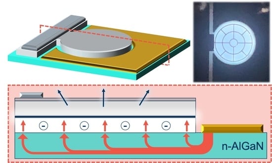
Figure 7.
A 284 nm UV LED employing the n-AlGaN layer described in this report. (a) Voltage and output power versus current, inset: spectrum showing sharp peak at 284 nm, and no observable UV-A or visible parasitic emission. Operating voltage is below 8V, providing a voltage efficiency of 54% at 20 A/cm2. (b) External quantum efficiency (EQE) and wall plug efficiency (WPE) of the UV LED versus current density, inset: microscope image of operating UV LED showing uniform emission pattern with 500 μm scale bar.

Publisher’s Note: MDPI stays neutral with regard to jurisdictional claims in published maps and institutional affiliations. |
© 2021 by the authors. Licensee MDPI, Basel, Switzerland. This article is an open access article distributed under the terms and conditions of the Creative Commons Attribution (CC BY) license (https://creativecommons.org/licenses/by/4.0/).
Share and Cite
MDPI and ACS Style
Zollner, C.J.; Yao, Y.; Wang, M.; Wu, F.; Iza, M.; Speck, J.S.; DenBaars, S.P.; Nakamura, S. Highly Conductive n-Al0.65Ga0.35N Grown by MOCVD Using Low V/III Ratio. Crystals 2021, 11, 1006. https://doi.org/10.3390/cryst11081006
AMA Style
Zollner CJ, Yao Y, Wang M, Wu F, Iza M, Speck JS, DenBaars SP, Nakamura S. Highly Conductive n-Al0.65Ga0.35N Grown by MOCVD Using Low V/III Ratio. Crystals. 2021; 11(8):1006. https://doi.org/10.3390/cryst11081006
Chicago/Turabian StyleZollner, Christian J., Yifan Yao, Michael Wang, Feng Wu, Michael Iza, James S. Speck, Steven P. DenBaars, and Shuji Nakamura. 2021. "Highly Conductive n-Al0.65Ga0.35N Grown by MOCVD Using Low V/III Ratio" Crystals 11, no. 8: 1006. https://doi.org/10.3390/cryst11081006
Note that from the first issue of 2016, this journal uses article numbers instead of page numbers. See further details here.