Article

Optimization of Layer Transfer and Photolithography for Device Integration of 2D-TMDC

1
Compound Semiconductor Technology, RWTH Aachen University, Sommerfeldstraße 18, 52074 Aachen, Germany
2
AIXTRON SE, Dornkaulstr. 2, 52134 Herzogenrath, Germany
*
Author to whom correspondence should be addressed.
Crystals 2023, 13(10), 1474; https://doi.org/10.3390/cryst13101474
Submission received: 15 September 2023 / Revised: 6 October 2023 / Accepted: 8 October 2023 / Published: 10 October 2023

Abstract

:
Extensive research into two-dimensional transition metal dichalcogenides (2D-TMDCs) over the past decade has paved the way for the development of (opto)electronic devices with enhanced performance and novel capabilities. To realize devices based on 2D-TMDC layers, compatible and optimized technologies such as layer transfer and photolithography are required. Challenges arise due to the ultrathin, surface-only nature of 2D layers with weak van der Waals adhesion to their substrate. This might potentially compromise their integrity during transfer and photolithography processes, in which prolonged exposure at usually high temperature to reactive chemicals and strong solvents are conventionally used. In this paper, we show that employing a dry-transfer technique based on thermal release tape (TRT) as an alternative to wet processes based on KOH solution better preserves layer quality. In the succeeding device fabrication process, an optimized photolithography as a cost-effective and widely available method for device patterning is utilized. The introduced photolithography protocol presents a near-perfect yield and reproducibility. To validate our optimized techniques, we fabricated field-effect transistors (FETs) using 2D-MoS2 layers from metal–organic chemical vapor deposition (MOCVD), wet- and dry-transferred onto SiO2/Si substrates. Our findings mark a significant stride towards the efficient and industry-compatible utilization of 2D van der Waals materials in device fabrication.

1. Introduction

The exploration of two-dimensional transition metal dichalcogenides (2D-TMDCs) has ignited significant interest, paving the way for innovative advancements in (opto)electronic devices with intriguing performances and novel functionalities [1,2,3]. The applicability of these materials encompasses a wide range of fields including silicon complementary metal-oxide semiconductor (CMOS) scaling [2,4], neuromorphic computing [5], sensing [6], quantum technologies [7], photonics [8] and wearable electronics [9]. Their industrial implementation, however, calls for a series of adapted or new fabrication techniques [10].
The need for elevated growth temperature, chemically active precursors and promoters [11,12,13], coupled with the necessity for epitaxial growth, presents a challenge for the direct growth of 2D materials on technologically relevant substrates like Si. Consequently, a variety of methods have emerged to facilitate the transfer of 2D materials from their growth substrates to target wafers, each yielding varying degrees of contamination, non-uniformity and transfer-induced damage [14,15,16]. These transfer techniques are conventionally classified into “wet” and “dry” categories. While wet techniques involve the use of liquid-phase chemicals including water for delamination [17], in dry transfer, the 2D layer is delaminated from the growth substrate without direct exposure to water or other chemicals. Specifically, wet-transfer methods have been associated with the introduction of defects and impurities, including wrinkles, polymer residues and cracks [14,18,19]. In contrast, the dry-transfer technique has been demonstrated to preserve the quality of the as-grown layers, while also offering inherent scalability to larger areas [19,20,21]. Notably, the majority of research on dry-transfer techniques for 2D layers has focused on graphene, with relatively few investigations dealing with 2D-TMDCs. Furthermore, a direct comparison regarding the electrical properties and device performance of 2D-TMDC layers achieved through wet- and dry-transfer methods is lacking.
For patterning and device definition, photoresist-based conventional photolithography is optimized for traditional semiconductors. However, such processes are not readily applicable to 2D-TMDC layers due to several inherent challenges. The susceptibility of these atomically thin layers to detachment or impairment by typical chemical agents and strong solvents, especially when exposed to high temperatures for extended periods, poses a significant obstacle. Consequently, a tailored patterning technique specific to 2D-TMDCs layers is in high demand. Various patterning techniques have been explored thus so far [10,15,22,23]. However, the reported approaches either suffer from notable drawbacks or do not fulfill the requirements for patterning 2D-TMDC materials. For instance, the photolithography process introduced by Zhang et al. [23] was exclusively demonstrated using mechanically exfoliated small TMDC flakes which exhibit considerable differences to wafer-scale 2D-TMDC layers produced through methods like chemical vapor deposition (CVD) or metal–organic CVD (MOCVD). These differences encompass properties such as layer uniformity, defect densities, and interactions with the substrate [24,25,26]. Such disparities significantly impact layer stability during the fabrication process, which may raise concerns about the applicability of the introduced methods to the wafer-scale synthetic 2D-TMDC layers. Furthermore, protocols involving photolithography with polymethyl methacrylate (PMMA) as resist and Irgacure as an additive for photosensitization of PMMA exhibit poor reproducibility when applied to the fabrication of devices based on 2D-TMDC materials [27]. Other reported patterning techniques such as e-beam lithography or focused-laser writing also possess various limitations. For instance, the former demands an ultra-high vacuum condition, coupled with low yield and throughput, while the latter features substrate dependency and low resolution due to the large spot diameter of the laser [15,28,29].
Addressing these challenges, this study explores the efficacy of a dry-transfer technique utilizing thermal release tape (TRT) as an alternative to the conventional wet process involving potassium hydroxide (KOH) solution. Furthermore, an optimized photolithography process with near-perfect yield and reproducibility is introduced. The validation of these refined techniques is showcased through the successful fabrication of globally back-gated field-effect transistors (FETs) based on MOCVD 2D-MoS2 layers.

2. Materials and Methods

Two-dimensional molybdenum disulfide (2D-MoS2) was epitaxially grown on sapphire (0001) substrates using a commercial AIXTRON reactor in 10 × 2″ configuration. The process started with a substrate prebake at 1050 °C in a pure H2 atmosphere, to promote lateral growth in the following growth phase [30]. Deposition was performed at a temperature of 845 °C, employing di-tert-butyl sulfide (DTBS) and molybdenum hexacarbonyl (Mo(CO)6) as sulfur and molybdenum precursors and N2 as the carrier gas at 30 hPa total reactor pressure. A high sulfur-to-molybdenum precursor ratio of 20,000 was adopted. To achieve this, the precursor flows have been set to 0.1 nmol/min for Mo(CO)6 and 20 µmol/min for DTBS.
The as-deposited and processed layers were analyzed through Raman spectroscopy (Renishaw, 532 nm laser line, 1 mW) and atomic-force microscopy (AFM). AFM measurements were performed in contact mode using a DME DualScope C-26 system.
Globally back-gated field-effect transistors (FETs) were fabricated for electrical characterization of the wet- and dry-transferred layers. Initially the layers were transferred from growth substrate (sapphire) to the target substrate (highly p-doped Si with 1–10 Ω·cm specific resistivity and 100 nm thermally grown SiO2). For wet transfer, 1 M KOH (Th. Geyer Co., Renningen, Germany) in deionized (DI) water and for the dry transfer Nitto Revalpha (P/N 319Y-4LS) thermal release tape (TRT) were used. For both approaches, the support layer consists of PMMA (950 PMMA A6, Kayaku Advanced Material, Inc., Westborough, MA, USA). For photolithography, AZ 5214 E image reversal photoresist (Merck Performance Material GmbH, Wiesbaden, Germany), lift-off resist (LOR, KAYAKU Advanced Material) and AZ 726 MIF developer (Microchemical, Ulm, Germany) were used. Ultimately, the electrical measurements of transistors were performed in atmosphere at room temperature in the dark. More details on the fabrication process will be discussed in the following sections.

3. Results and Discussions

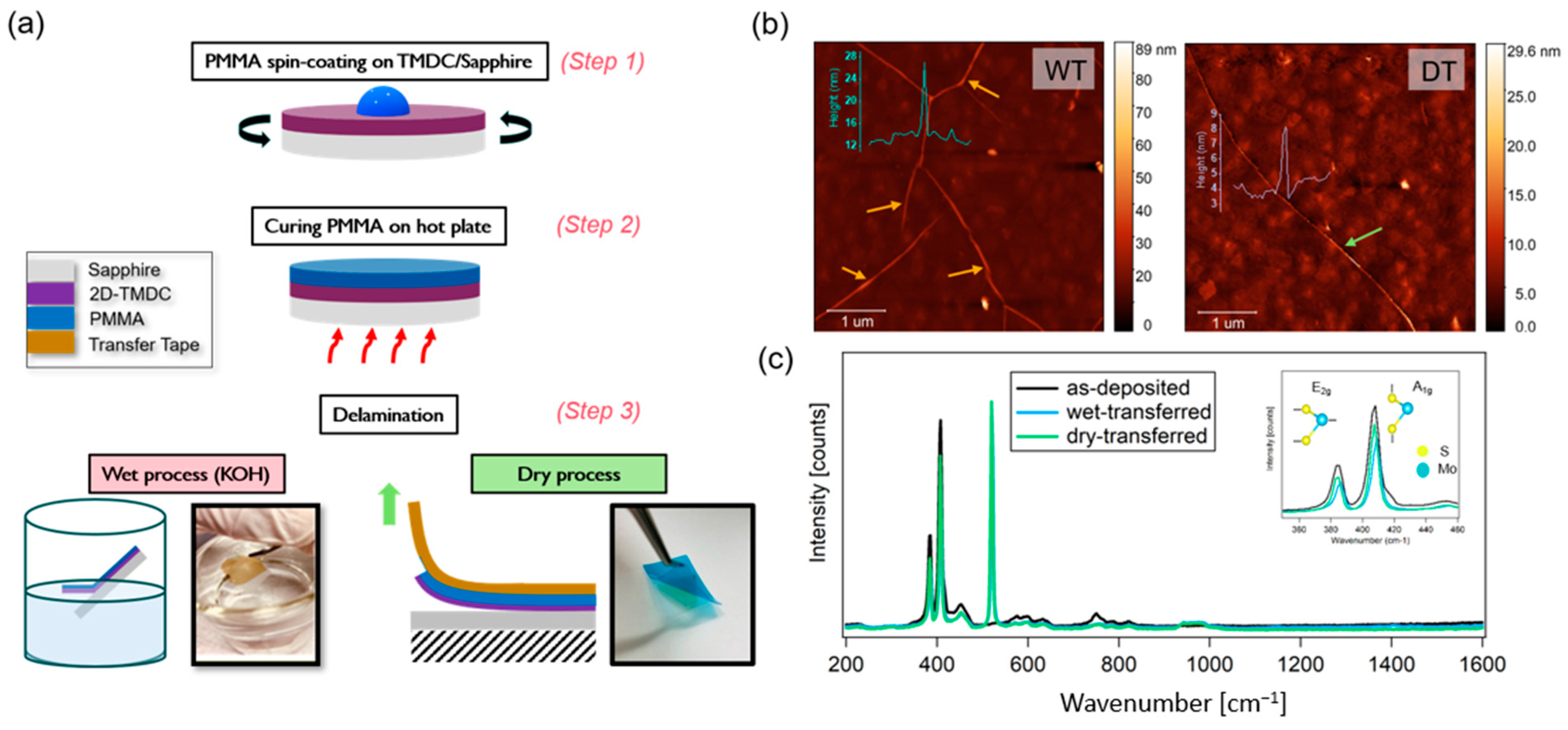
3.1. Wet and Dry Transfer of 2D-TMDC Layer

The wet and dry delamination processes are schematically illustrated in Figure 1a. The PMMA support layer was first spin-coated on the as-grown 2D-MoS2 on sapphire substrate with 3000 rpm for 30 s followed by a curing process at 120 °C for 10 min on a hot-plate in ambient air (Figure 1a, steps 1 and 2). The wafer was then cut into smaller pieces by mechanical cleavage. Despite the natural tendency of the aqueous KOH solution to penetrate between 2D-MoS2 layer and the sapphire substrate due to different surface energies, the delamination may not spontaneously start because of the intimate adhesion of the (MO)CVD layer with the substrate [14,26].
Such strong adhesion of the 2D-TMDC layer to the sapphire as the growth substrate could arise from the localized interaction of the defects with substrate [26]. This might lead to lower yield of the process in both wet and dry approaches. However, to facilitate the delamination, the edge of the sample can be scratched with a tweezer to form a gap between the 2D-TMDC and the substrate [16].
For delamination, only the scratched sample edge has to be immersed in the KOH solution. Detachment advances as the solution penetrates between 2D-TMDC and sapphire, causing the released section of the stack to gradually float on the solution (see Figure 1a, step 3 left) until complete release. It is worth mentioning that the angle through which the stack comes in contact with the solution is also of importance. The larger the angle, the faster the delamination occurs, but on the other hand, it introduces more wrinkles and transfer-induced damages to the layer. Our experiments suggest that a good choice is 30° to 45°. Next, the 2D-TMDC/PMMA film was carefully transferred to another beaker containing pure DI water to remove KOH contaminations. For this transfer, a clean sapphire wafer was used to gently scoop the floating sample from the liquid and releasing it again by immersion. This process was then repeated with another DI water beaker 3–4 times to ensure thorough cleansing of remaining KOH contamination. Finally, the 2D-PMMA stack was transferred onto the target (p++Si with 100 nm SiO2) substrate. The stack was left in the cleanroom overnight for drying. Following the drying step, the sample was baked for an additional 15 min at 120 °C in air to effectively eliminate any remaining moisture and enhance the adhesion between 2D layer and Si substrate. Subsequently, the PMMA layer was removed by immersing the sample in 80 °C acetone for 1 h.
For the dry transfer, following the previously mentioned method of creating a crack by carefully scratching the sample edge with tweezer, a piece of TRT was applied onto the sample. Subsequently, a gentle mechanical peel-off was initiated by carefully removing the tape, starting from the previously scratched edge (Figure 1a, step 3 right). Our observations indicated that the adhesion force between the TRT and PMMA typically surpasses that between the 2D layer and the substrate, resulting in an attempt success rate of about 90%. The released 2D/PMMA/TRT stack was then gently placed on the target substrate. The stack was then heated to the TRT release temperature of ≈100 °C on a hot-plate. After removing the tape, the sample temperature was raised to 150 °C to enhance the adhesion between 2D film and target substrate. Finally, 80 °C acetone was employed to remove the PMMA, following a procedure similar to that outlined above for the wet transfer. It was observed that the procedure for PMMA removal using hot acetone could occasionally result in some 2D layer loss in the case of dry transfer, unlike in wet transfer. This discrepancy might be attributed to the comparatively weaker adhesion of the 2D layer to the target substrate for dry-transferred layers.
The surface morphologies of the wet- and dry-transferred layers were examined using AFM (Figure 1b). Wet-transferred layers exhibited wrinkles up to 100 nm in height. In contrast, the dry-transferred layers appeared to be virtually wrinkle-free. Nonetheless, some areas displayed crack-like features, which are believed to stem from mechanical damage during the peel-off process.
Raman spectra of the as-deposited as well as the wet- and dry-transferred layers are depicted in Figure 1c. The characteristic MoS2 Raman peaks, namely E2g and A1g, were observed [31]. The corresponding peaks for as-deposited layer were found to be at ≈384.4 and ≈407.4 cm−1, respectively. Their separation was found to be 22.9 cm−1 which indicates a dominance of bi-layer and tri-layer MoS2 [32].
The spectra revealed a slight reduction in the intensity for both transferred layers, indicating some transfer-induced degradation. This intensity drop was comparatively less pronounced in the dry-transferred layer compared to the wet-transferred counterpart, suggesting that the former process could better preserve layer quality. Furthermore, the A1g peak exhibited 1 cm−1 and 2 cm−1 shifts toward higher wavenumbers in dry- and wet-transferred layers, respectively, in line with findings previously reported by Sharma et al. [33]. This shift might be attributed to the presence of PMMA residues on the surface which restrain the out-of-plane vibrational mode and introduce compressive strain along the c direction of the unit cell [34].

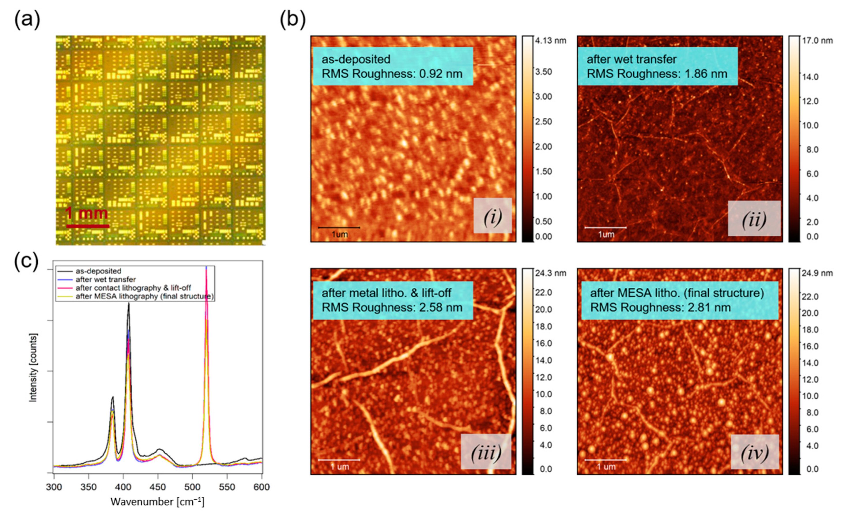
3.2. Photolithography of 2D-TMDC Layer

Preserving the integrity of 2D-TMDC layers during device processing requires careful consideration of the lithography sequence. It is essential to start with metal contact lithography before proceeding to MESA lithography. Initiating the process with MESA lithography would result in the exposure of smaller specially separated 2D areas, corresponding to the size of MESA (device) structures. These would have comparatively reduced stability when exposed to AZ 726 MIF or dimethyl sulfoxide (DMSO) solvents, triggering delamination and curling of the 2D layer in the subsequent steps. Examples of failed process steps will be given later in this section.
The photolithography process steps, including contact and MESA lithography followed by reactive ion etching (RIE) are shown in Figure 2.
For contact lithography, an image reversal process was employed. To execute this, an initial spin-coating of the LOR was performed at 5000 rpm for 30 s, followed by baking at 150 °C for 5 min. After allowing 2–3 min resting period, AZ5214 E photoresist was spin-coated at 4000 rpm for 30 s, followed by baking at 101 °C for 1 min.
Using a mask aligner, ultraviolet (UV) light of 25 mJ·cm−2 dose was used for sample exposure. Following an additional 10 min resting interval, post-exposure baking (PEB) was conducted at 118 °C for 1 min. Subsequently, flood exposure was conducted using a dose of 377 mJ·cm−2. The sample was then manually immersed in AZ 726 MIF developer for 70 s. Afterward, soaking in pure DI water was performed to eliminate any residual developer from the surface. Finally, the sample was gently blown with N2 flow to remove any DI water residues. Our experiments revealed that employing an automated developer with a high spin-speed could potentially introduce damage to the 2D layer. Additionally, it was found that using LOR/AZ5214 E as a double-layer resist not only provides a better undercut during development and subsequently facilitates lift off, but also enhances the efficiency of stripping using AZ 726 MIF developer (after the MESA etching step).
Following the deposition of an 80 nm Au layer by e-beam evaporation, the lift-off process was performed. For this purpose, the sample was manually immersed in room temperature DMSO. After an 8–9 min soaking period in the solvent, a syringe was employed to gently blow the surface, facilitating metal lift-off. Subsequently, the sample was rinsed in a fresh DMSO to eliminate any residual metal particles. To protect the delicate 2D layer from the impact of strong solvents, unlike e.g., compound semiconductors [35], it is essential to avoid prolonged exposure or subjecting the sample to high-temperature DMSO treatment. The failed process due to using high temperature DMSO is shown later in this section. The sample was then transferred to a circulating DI water pool to effectively clean any remaining DMSO residues. Next, the sample was rinsed in acetone and isopropanol (IPA), followed by N2 blowing. The final structure after ohmic contact lithography and lift off is presented in Figure 2(iii).
For MESA lithography, a positive process was utilized. To perform MESA lithography, the LOR and AZ5214 E photoresist were spin-coated and baked on the sample consecutively in a similar way explained for contact lithography. Optical lithography was performed with a dose of 160 mJ·cm−2. Finally, after a few minutes rest, the manual development was carried out for 30 s in AZ 726 MIF. Subsequently, an inductively coupled plasma (ICP) system with BCl3/Ar gas mixture was employed for dry etching the unprotected area and therefore isolating the device structures (Figure 2(iv)). The BCl3 and Ar gas flows were set to be 20 and 10 standard cubic centimeters per minutes (sccm), respectively. Afterwards, the photoresist mask was stripped away by immersing the sample for 1 min in the developer. The sample was then cleaned and dried in a similar way as explained before. Our experiments have shown that using DMSO or automated developer using AZ 726 MIF can potentially cause damage to the structures. Therefore, an immersion of the sample into AZ 726 MIF for stripping is strongly recommended.
An overview of the final structure is depicted in Figure 3a. The process demonstrated an exceptional yield of nearly 100%. Analyzing the surface topography evolution of the 2D-TMDC layer after each photolithography step reveals a slight increase in roughness, likely attributed to resist residues. Notably, the 2D layer maintains its integrity throughout the entire process, underscoring the gentle nature of the introduced photolithography method. However, a subtle decline in layer quality can be discerned from the measured Raman intensity spectra taken from the channel area after each photolithography step, as illustrated in Figure 3c.
Examples of processing failure scenarios are illustrated in Figure 4. Figure 4(i) highlights an instance of failure arising from exposure of isolated MESA (device) areas to DMSO during lift-off, which can be largely avoided by adjusting lithography sequences, as explained previously. Figure 4(ii,iii) show examples of processing failure attributed to extended exposure (30 min) or elevated temperature (105 °C) DMSO treatment during the lift-off step. Figure 4(iv) illustrates an unsuccessful attempt to strip the resist mask using developer after the MESA etching step in the absence of LOR. This highlights the fact that LOR also enables efficient stripping using AZ MIF developer. In Figure 4(v,vi) the TRT release steps are depicted. An example of failure of the tape during release at ≈100 °C temperature can be seen in (v). In this case, the adhesive part of the tape strongly adhered to the PMMA/2D stack and detaches it from the Si substrate when lifting the tape. This can lead to partial or complete loss of 2D material. TRT failure similar to the scenario shown in Figure 4(v) was rarely observed during our experiments. In Figure 4(vi), a successful TRT release is demonstrated. In this case, no PMMA/2D residues can be found on the released tape. Figure 4(vii) depicts a scenario in which a loss of the 2D layer occurred after dry transfer and during PMMA acetone cleaning. This can be attributed to the weak adhesion between the 2D layer and the target substrate in the dry-transfer case. This particular challenge remains a bottleneck in dry-transfer processes, requiring further investigations. Additionally, Figure 4(viii) demonstrates a successful dry transfer, during which the 2D layer could survive the hot acetone PMMA cleaning.

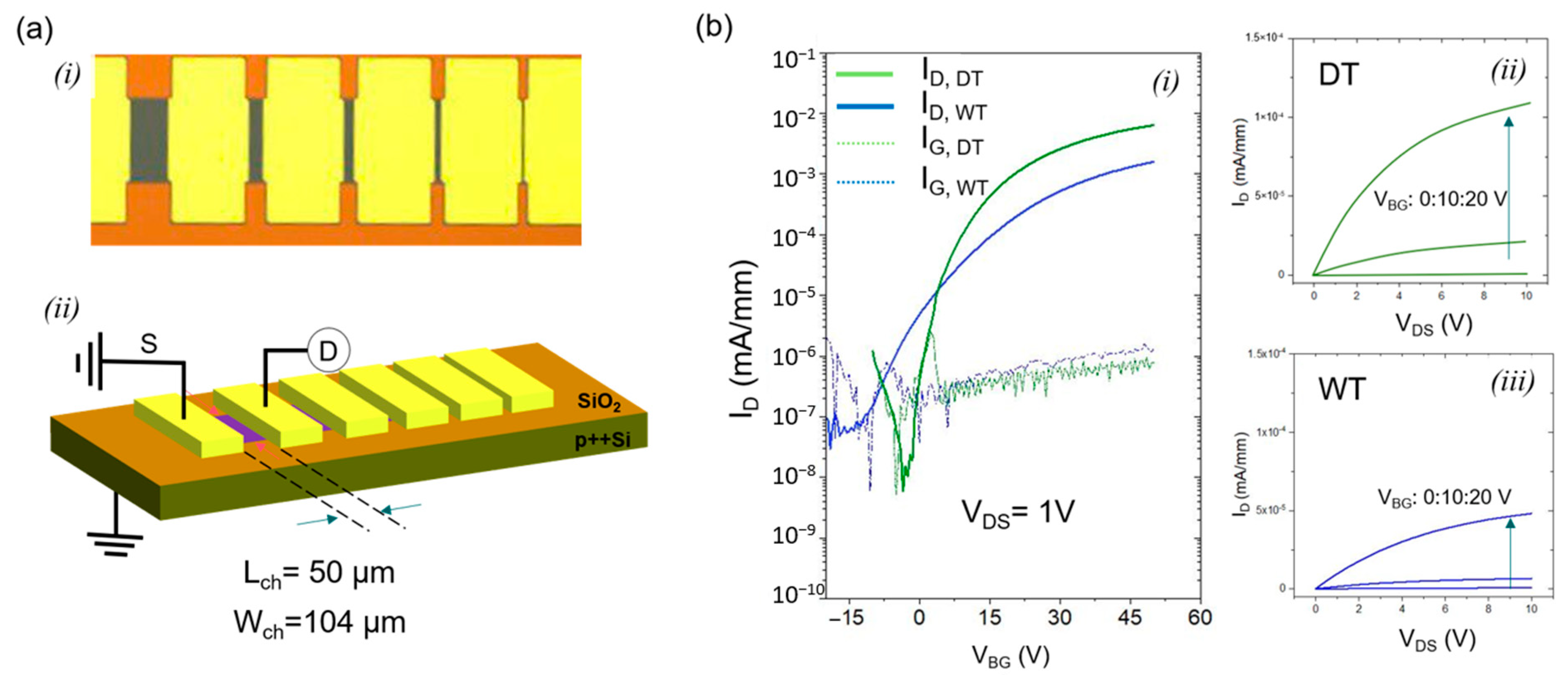
3.3. Electrical Characterization of Wet- and Dry-Transferred 2D-MoS2 Layers

Using the optimized photolithography technique discussed in the previous section, electrical devices based on both wet- and dry-transferred 2D-MoS2 layers were fabricated. Au was chosen as contact metal, the highly p-type doped Si substrate used as a global back gate with 100 nm thermally grown SiO2 layer as the gate dielectric. An optical image of a transfer length method (TLM) structure is shown in Figure 5a(i), and its layout is schematically illustrated in Figure 5a(ii). The filed-effect mobility values were calculated based on Equation (1) [36,37]:
μ FE = I D V B G . 1 V D S . L W . d o x ε r , o x ε 0
Here, ID is the drain current, VBG is the back-gate voltage, VDS is the drain–source voltage, L and W are the channel length and width, respectively, dox is the gate oxide thickness, εr,ox = 3.9 is the relative permittivity of the gate oxide (SiO2), and ε0 is the vacuum permittivity. The transfer characteristics of the wet- and dry-transferred layers, along with their corresponding gate leakage currents are shown in Figure 5b(i). The wet-transferred 2D-MoS2 layer exhibits a mobility (µFE) of 0.056 cm2/V·s, while its dry-transferred counterpart demonstrates a significantly enhanced mobility of 0.271 cm2/V·s. Additionally, the Ion/Ioff ratios were found to be 104 and 106 for wet- and dry-transferred layers, respectively, highlighting a substantial improvement in the case of dry transfer. Moreover, the subthreshold swing ( S S = d I D / d l o g 10 I D ) [38] was calculated and found to be 584 and 137 mV/decade for wet- and dry-transferred layers, respectively. In Figure 5b(ii,iii), the output characteristics of the devices are presented. Both devices based on wet- and dry-transferred layers show saturation at the given back-gate voltages, indicating ideal transistors operation behavior. However, for dry-transferred samples, the obtained current at a similar gate voltage, i.e., 20 V, is one order of magnitude higher than that for wet-transferred counterpart. This significant improvement underscores the enhanced electrical performance of the dry transferred layers.
Figure 5. (a) Device structures (i) optical image of the fabricated TLM structure, (ii) schematic of the contacts and the channel, used to extract the electrical properties. (b) The measured (i) transfer characteristic and (ii,iii) the output characteristic of 2D-MoS2 layer, DT: dry transfer, WT: wet transfer.
Crystals 13 01474 g005
A significant improvement in electrical performance seen for dry-transferred layers can be attributed to the absence of KOH-related contamination and degradation effects present in wet transfer process. Wet transfer was shown to cause wrinkles, cracks and other damage to a larger extent than dry transfer, negatively affecting charge transport and device characteristics. Dry transfer process using a TRT eliminates solution-transfer-related issues, ensuring a cleaner material. This cleaner layer coupled with reduced structural damages (i.e., wrinkles) leads to a superior charge carrier mobility and transport properties, contributing to the observed improvement in electrical performance metrics like, mobility, saturation behavior, Ion/Ioff ratio and subthreshold swing.
It worth noting that both wet- and dry-transferred 2D-MoS2 layers in this study exhibit lower device performance compared to levels commonly published in literature. For example, the field-effect mobility for MOCVD 2D-MoS2 is typically reported around 15–20 cm2/V·s [39,40], which is approximately two orders of magnitude higher than the maximum value observed in our work. The reduced device performance in this study, regardless of the transfer technique employed can be primarily attributed to the unoptimized MOCVD process, leading to the formation of a significant density of grain boundaries and defects (e.g., vacancies), which are well-known factors deteriorating charge transport in the device channel [41,42] and lead to a high contact resistance [43,44].

4. Conclusions

In this study, two fundamental steps of 2D-TMDC device processing, namely layer transfer and photolithography, were investigated and improved. The wet- and dry-transfer methods were carefully examined and compared utilizing AFM and Raman spectroscopy. Dry transfer is demonstrated to be superior owing to prevention of wrinkle formation and higher structural quality of transferred layers. An optimization of the photolithography process for 2D-TMDC-based devices was also carried out. The significance of the lithography step order and the requirement for low-temperature DMSO treatment during metal lift-off were underscored. This enhanced material quality directly translates into improved device performance of field-effect transistors such as mobility and Ion/Ioff ratio.

Author Contributions

Conceptualization, A.G. (Amir Ghiami); Data curation, T.S.; Funding acquisition, A.V.; Investigation, T.S., H.F., S.T. and A.G. (Annika Grundmann); Methodology, A.G. (Amir Ghiami) and T.S.; Supervision, M.H. and A.V.; Validation, H.K.; Visualization, A.G. (Amir Ghiami) and T.S.; Writing—original draft, A.G. (Amir Ghiami); Writing—review and editing, H.K. All authors have read and agreed to the published version of the manuscript.

Funding

This work has been financially supported by the Federal Ministry of Education and Research (BMBF), NEUROTEC-II and NeuroSys projects, no. 16ME0399 and 03ZU1106AA.

Data Availability Statement

All the data are available in the article.

Conflicts of Interest

The authors declare no conflict of interest.

References

  1. Lemme, M.C.; Akinwande, D.; Huyghebaert, C.; Stampfer, C. 2D materials for future heterogeneous electronics. Nat. Commun. 2022, 13, 1392. [Google Scholar] [CrossRef] [PubMed]
  2. Wang, C.; Song, Y.; Huang, H. Evolution Application of Two-Dimensional MoS2-Based Field-Effect Transistors. Nanomaterials 2022, 12, 3233. [Google Scholar] [CrossRef] [PubMed]
  3. Dutta, T.; Yadav, N.; Wu, Y.; Cheng, G.J.; Liang, X.; Ramakrishna, S.; Sbai, A.; Gupta, R.; Mondal, A.; Hongyu, Z.; et al. Electronic properties of 2D materials and their junctions. Nano Mater. Sci. 2023. [Google Scholar] [CrossRef]
  4. Lanza, M.; Radu, I. Electronic Circuits made of 2D Materials. Adv. Mater. 2022, 34, 4–7. [Google Scholar] [CrossRef] [PubMed]
  5. Cao, G.; Meng, P.; Chen, J.; Liu, H.; Bian, R.; Zhu, C.; Liu, F.; Liu, Z. 2D Material Based Synaptic Devices for Neuromorphic Computing. Adv. Funct. Mater. 2021, 31, 2005443. [Google Scholar] [CrossRef]
  6. Ping, J.; Fan, Z.; Sindoro, M.; Ying, Y.; Zhang, H. Recent Advances in Sensing Applications of Two-Dimensional Transition Metal Dichalcogenide Nanosheets and Their Composites. Adv. Funct. Mater. 2017, 27, 1605817. [Google Scholar] [CrossRef]
  7. Pal, A.; Zhang, S.; Chavan, T.; Agashiwala, K.; Yeh, C.; Cao, W.; Banerjee, K. Quantum-Engineered Devices Based on 2D Materials for Next-Generation Information Processing and Storage. Adv. Mater. 2023, 35, e2109894. [Google Scholar] [CrossRef]
  8. Mak, K.F.; Shan, J. Photonics and optoelectronics of 2D semiconductor transition metal dichalcogenides. Nat. Photonics 2016, 10, 216–226. [Google Scholar] [CrossRef]
  9. Yao, J.; Yang, G. 2D group 6 transition metal dichalcogenides toward wearable electronics and optoelectronics. J. Appl. Phys. 2020, 127, 030902. [Google Scholar] [CrossRef]
  10. Jia, L.; Wu, J.; Zhang, Y.; Qu, Y.; Jia, B.; Chen, Z.; Moss, D.J. Fabrication Technologies for the On-Chip Integration of 2D Materials. Small Methods 2022, 6, 2101435. [Google Scholar] [CrossRef]
  11. Tang, S.; Grundmann, A.; Fiadziushkin, H.; Wang, Z.; Hoffmann-Eifert, S.; Ghiami, A.; Debald, A.; Heuken, M.; Vescan, A.; Kalisch, H. Migration-Enhanced Metal–Organic Chemical Vapor Deposition of Wafer-Scale Fully Coalesced WS 2 and WSe 2 Monolayers. Cryst. Growth Des. 2023, 23, 1547–1558. [Google Scholar] [CrossRef]
  12. Chubarov, M.; Choudhury, T.H.; Hickey, D.R.; Bachu, S.; Zhang, T.; Sebastian, A.; Bansal, A.; Zhu, H.; Trainor, N.; Das, S.; et al. Wafer-Scale Epitaxial Growth of Unidirectional WS 2 Monolayers on Sapphire. ACS Nano 2021, 15, 2532–2541. [Google Scholar] [CrossRef] [PubMed]
  13. Zhou, H.; Wang, C.; Shaw, J.C.; Cheng, R.; Chen, Y.; Huang, X.; Liu, Y.; Weiss, N.O.; Lin, Z.; Huang, Y.; et al. Large Area Growth and Electrical Properties of p-Type WSe 2 Atomic Layers. Nano Lett. 2015, 15, 709–713. [Google Scholar] [CrossRef] [PubMed]
  14. Gurarslan, A.; Yu, Y.; Su, L.; Yu, Y.; Suarez, F.; Yao, S.; Zhu, Y.; Ozturk, M.; Zhang, Y.; Cao, L. Surface-energy-assisted perfect transfer of centimeter-scale monolayer and few-layer MoS2 films onto arbitrary substrates. ACS Nano 2014, 8, 11522–11528. [Google Scholar] [CrossRef] [PubMed]
  15. Weinhold, M.; Klar, P.J. Patterning 2D materials for devices by mild lithography. RSC Adv. 2021, 11, 29887–29895. [Google Scholar] [CrossRef]
  16. Shen, Y.; Wu, Y.; Lee, L.; Chen, J.; Wani, S.S.; Yang, T.; Luo, C.W.; Siao, M.; Yu, Y.; Chiu, P.; et al. Rational Design on Wrinkle-Less Transfer of Transition Metal Dichalcogenide Monolayer by Adjustable Wettability-Assisted Transfer Method. Adv. Funct. Mater. 2021, 31, 2104978. [Google Scholar] [CrossRef]
  17. Watson, A.J.; Lu, W.; Guimarães, M.H.D.; Stöhr, M. Transfer of large-scale two-dimensional semiconductors: Challenges and developments. 2D Mater. 2021, 8, 032001. [Google Scholar] [CrossRef]
  18. Lin, Z.; Zhao, Y.; Zhou, C.; Zhong, R.; Wang, X.; Tsang, Y.H.; Chai, Y. Controllable Growth of Large–Size Crystalline MoS2 and Resist-Free Transfer Assisted with a Cu Thin Film. Sci. Rep. 2015, 5, 18596. [Google Scholar] [CrossRef]
  19. Yoon, M.-A.; Kim, C.; Kim, J.-H.; Lee, H.-J.; Kim, K.-S. Surface Properties of CVD-Grown Graphene Transferred by Wet and Dry Transfer Processes. Sensors 2022, 22, 3944. [Google Scholar] [CrossRef]
  20. Yoon, T.; Shin, W.C.; Kim, T.Y.; Mun, J.H.; Cho, B.J. Direct Measurement of Adhesion Energy of Monolayer Graphene As-Grown on Copper and Its Application to Renewable Transfer Process. Nano Lett. 2012, 12, 1448–1452. [Google Scholar] [CrossRef]
  21. Kim, C.; Yoon, M.-A.; Jang, B.; Kim, H.-D.; Kim, J.-H.; Hoang, A.T.; Ahn, J.-H.; Jung, H.-J.; Lee, H.-J.; Kim, K.-S. Damage-free transfer mechanics of 2-dimensional materials: Competition between adhesion instability and tensile strain. NPG Asia Mater. 2021, 13, 44. [Google Scholar] [CrossRef]
  22. Shi, Y.; Taniguchi, T.; Byun, K.-N.; Kurimoto, D.; Yamamoto, E.; Kobayashi, M.; Tsukagoshi, K.; Osada, M. Damage-free LED lithography for atomically thin 2D material devices. Sci. Rep. 2023, 13, 2583. [Google Scholar] [CrossRef] [PubMed]
  23. Zhang, R.; Chen, T.; Bunting, A.; Cheung, R. Optical lithography technique for the fabrication of devices from mechanically exfoliated two-dimensional materials. Microelectron. Eng. 2016, 154, 62–68. [Google Scholar] [CrossRef]
  24. Hong, J.; Hu, Z.; Probert, M.; Li, K.; Lv, D.; Yang, X.; Gu, L.; Mao, N.; Feng, Q.; Xie, L.; et al. Exploring atomic defects in molybdenum disulphide monolayers. Nat. Commun. 2015, 6, 6293. [Google Scholar] [CrossRef] [PubMed]
  25. Plechinger, G.; Mann, J.; Preciado, E.; Barroso, D.; Nguyen, A.; Eroms, J.; Schüller, C.; Bartels, L.; Korn, T. A direct comparison of CVD-grown and exfoliated MoS2 using optical spectroscopy. Semicond. Sci. Technol. 2014, 29, 064008. [Google Scholar] [CrossRef]
  26. Kang, K.; Lee, K.-H.; Han, Y.; Gao, H.; Xie, S.; Muller, D.A.; Park, J. Layer-by-layer assembly of two-dimensional materials into wafer-scale heterostructures. Nature 2017, 550, 229–233. [Google Scholar] [CrossRef]
  27. Carbaugh, D.J.; Wright, J.T.; Parthiban, R.; Rahman, F. Photolithography with polymethyl methacrylate (PMMA). Semicond. Sci. Technol. 2016, 31, 025010. [Google Scholar] [CrossRef]
  28. Shautsova, V.; Sinha, S.; Hou, L.; Zhang, Q.; Tweedie, M.; Lu, Y.; Sheng, Y.; Porter, B.F.; Bhaskaran, H.; Warner, J.H. Direct Laser Patterning and Phase Transformation of 2D PdSe 2 Films for On-Demand Device Fabrication. ACS Nano 2019, 13, 14162–14171. [Google Scholar] [CrossRef]
  29. Lin, L.; Li, J.; Li, W.; Yogeesh, M.N.; Shi, J.; Peng, X.; Liu, Y.; Rajeeva, B.B.; Becker, M.F.; Liu, Y.; et al. Optothermoplasmonic Nanolithography for On-Demand Patterning of 2D Materials. Adv. Funct. Mater. 2018, 28, 1803990. [Google Scholar] [CrossRef]
  30. Marx, M.; Nordmann, S.; Knoch, J.; Franzen, C.; Stampfer, C.; Andrzejewski, D.; Kümmell, T.; Bacher, G.; Heuken, M.; Kalisch, H.; et al. Large-area MoS2 deposition via MOVPE. J. Cryst. Growth 2017, 464, 100–104. [Google Scholar] [CrossRef]
  31. Mignuzzi, S.; Pollard, A.J.; Bonini, N.; Brennan, B.; Gilmore, I.S.; Pimenta, M.A.; Richards, D.; Roy, D. Effect of disorder on Raman scattering of single-layer MoS2. Phys. Rev. B 2015, 91, 195411. [Google Scholar] [CrossRef]
  32. Li, H.; Zhang, Q.; Yap, C.C.R.; Tay, B.K.; Edwin, T.H.T.; Olivier, A.; Baillargeat, D. From Bulk to Monolayer MoS2: Evolution of Raman Scattering. Adv. Funct. Mater. 2012, 22, 1385–1390. [Google Scholar] [CrossRef]
  33. Sharma, M.; Singh, A.; Singh, R. Monolayer MoS2 Transferred on Arbitrary Substrates for Potential Use in Flexible Electronics. ACS Appl. Nano Mater. 2020, 3, 4445–4453. [Google Scholar] [CrossRef]
  34. Zhang, Y.; Liu, J.; Pan, Y.; Luo, K.; Yu, J.; Zhang, Y.; Jia, K.; Yin, H.; Zhu, H.; Tian, H.; et al. The evolution of MoS2 properties under oxygen plasma treatment and its application in MoS2 based devices. J. Mater. Sci. Mater. Electron. 2019, 30, 18185–18190. [Google Scholar] [CrossRef]
  35. Saranovac, T.; Ruiz, D.C.; Han, D.; Arabhavi, A.M.; Ostinelli, O.; Bolognesi, C.R. Effects of electrochemical etching on InP HEMT fabrication. IEEE Trans. Semicond. Manuf. 2019, 32, 496–501. [Google Scholar] [CrossRef]
  36. Jing, X.; Illarionov, Y.; Yalon, E.; Zhou, P.; Grasser, T.; Shi, Y.; Lanza, M. Engineering Field Effect Transistors with 2D Semiconducting Channels: Status and Prospects. Adv. Funct. Mater. 2020, 30, 1901971. [Google Scholar] [CrossRef]
  37. Mitta, S.B.; Choi, M.S.; Nipane, A.; Ali, F.; Kim, C.; Teherani, J.T.; Hone, J.; Yoo, W.J. Electrical characterization of 2D materials-based field-effect transistors. 2D Mater. 2021, 8, 012002. [Google Scholar] [CrossRef]
  38. Yoon, Y.; Ganapathi, K.; Salahuddin, S. How Good Can Monolayer MoS2 Transistors Be? Nano Lett. 2011, 11, 3768–3773. [Google Scholar] [CrossRef]
  39. Shi, Y.; Groven, B.; Serron, J.; Wu, X.; Mehta, A.N.; Minj, A.; Sergeant, S.; Han, H.; Asselberghs, I.; Lin, D.; et al. Engineering Wafer-Scale Epitaxial Two-Dimensional Materials through Sapphire Template Screening for Advanced High-Performance Nanoelectronics. ACS Nano 2021, 15, 9482–9494. [Google Scholar] [CrossRef]
  40. Cun, H.; Macha, M.; Kim, H.; Liu, K.; Zhao, Y.; LaGrange, T.; Kis, A.; Radenovic, A. Wafer-scale MOCVD growth of monolayer MoS2 on sapphire and SiO2. Nano Res. 2019, 12, 2646–2652. [Google Scholar] [CrossRef]
  41. Giannazzo, F.; Bosi, M.; Fabbri, F.; Schilirò, E.; Greco, G.; Roccaforte, F. Direct Probing of Grain Boundary Resistance in Chemical Vapor Deposition-Grown Monolayer MoS2 by Conductive Atomic Force Microscopy. Phys. Status Solidi Rapid Res. Lett. 2020, 14, 1900393. [Google Scholar] [CrossRef]
  42. Yu, Z.; Pan, Y.; Shen, Y.; Wang, Z.; Ong, Z.-Y.; Xu, T.; Xin, R.; Pan, L.; Wang, B.; Sun, L.; et al. Towards intrinsic charge transport in monolayer molybdenum disulfide by defect and interface engineering. Nat. Commun. 2014, 5, 5290. [Google Scholar] [CrossRef]
  43. Giannazzo, F.; Fisichella, G.; Piazza, A.; Di Franco, S.; Greco, G.; Agnello, S.; Roccaforte, F. Impact of contact resistance on the electrical properties of MoS2 transistors at practical operating temperatures. Beilstein J. Nanotechnol. 2017, 8, 254–263. [Google Scholar] [CrossRef] [PubMed]
  44. Allain, A.; Kang, J.; Banerjee, K.; Kis, A. Electrical contacts to two-dimensional semiconductors. Nat. Mater. 2015, 14, 1195–1205. [Google Scholar] [CrossRef] [PubMed]
Figure 1. Comparison between wet- and dry-transfer techniques. (a) Schematic illustration of wet and dry delamination steps. (b) AFM of wet- (WT) and dry- (DT) transferred layers after PMMA removal. The arrows show the wrinkles and mechanical damage (crack) after WT and DT, respectively. The AFM height profiles across a wrinkle and a crack are also shown for WT and DT. (c) Raman spectra of as-deposited versus wet- and dry-transferred layers; the inset shows the zoomed-in spectra.
Crystals 13 01474 g001
Figure 2. Photolithography process steps. (i) transferred 2D-MoS2 on target substrate, (ii) after contact lithography and development, (iii) after metal evaporation and lift-off, (iv) after MESA lithography and development and (v) after reactive ion etching (final structure). The upper row shows the schematic illustration and the lower row shows the corresponding optical images.
Crystals 13 01474 g002
Figure 3. (a) Overview of the final structure (b) AFM topography of 2D-MoS2 layer: (i) as-deposited, (ii) after wet-transfer and PMMA cleaning, (iii) after contact lithography and lift-off and (iv) after consequent MESA lithography and photoresist stripping; (c) Raman spectra evolution of the 2D-MoS2 layer during photolithography steps.
Crystals 13 01474 g003
Figure 4. (i) 2D-TMDC layer detachment and curling during stripping; (ii,iii) metal contact and 2D-TMDC layer detachment and curling during lift-off. (iv) unsuccessful photoresist stripping (w/o LOR); TRT release step: (v) tape release failure, (vi) successful tape release; dry-transferred 2D-TMDC layer after PMMA cleaning: (vii) partial 2D-TMDC layer loss during PMMA cleaning, and (viii) completely survived 2D-TMDC layer during PMMA cleaning.
Crystals 13 01474 g004
Disclaimer/Publisher’s Note: The statements, opinions and data contained in all publications are solely those of the individual author(s) and contributor(s) and not of MDPI and/or the editor(s). MDPI and/or the editor(s) disclaim responsibility for any injury to people or property resulting from any ideas, methods, instructions or products referred to in the content.

