
Layered Structure Based on PANi and SiO2 to Absorb HPM to Protect Systems and Devices


International Centre for Radio Astronomy Research, Curtin University, Bentley, WA 6102, Australia
*
Author to whom correspondence should be addressed.
Crystals 2024, 14(5), 391; https://doi.org/10.3390/cryst14050391
Submission received: 1 April 2024
/
Revised: 18 April 2024
/
Accepted: 20 April 2024
/
Published: 23 April 2024
(This article belongs to the Special Issue Metamaterials and Metasurfaces for Microwave and THz Applications)
Abstract
:A layered structure composed of polyaniline (PANI) and silicon dioxide (SiO2) is proposed in this article. It was developed to obtain ultra-wideband and high-power microwave absorption. Due to the high thermal stability of PANi and SiO2 above 400 °C, the proposed structure is able to absorb high amounts of power. The electromagnetic behavior of the structure is examined by full-wave simulation to investigate its ability to absorb microwave frequencies ranging from 1 to 20 GHz under both normal and oblique incidences of electromagnetic waves. Recent studies have produced results with a limited absorption range and a less consistent angular incidence than the structure presently being examined. Also, the layer-by-layer deposition of thin film facilitates the manufacturing procedure. Furthermore, owing to the high thermal stability of the proposed structure, the absorption of high-power microwaves is superior to that of alternative methodologies.
1. Introduction
High-power microwaves (HPM) describe a group of electromagnetic (EM) devices that may produce bursts of powerful microwave radiation [1,2,3,4]. HPMs can reach a peak power of 100 MW and operate within the frequency range of 1–300 GHz [5]. According to research [6,7,8,9], HPM poses a severe risk to electronic systems and can interrupt or damage critical systems and infrastructure. HPM weapons can disrupt a wide range of unprotected electronic systems within their electromagnetic span, including those used by the military and commercial sectors [10,11]. These HPMs can produce high-amplitude current and voltage electrical pulses that last from a few nanoseconds to tens of nanoseconds [12]. Therefore, they can interfere with some electronic systems permanently or temporarily while others remain unharmed. Electromagnetic interference (EMI), sometimes called undesirable interruptions from outside sources, is often associated with the impact of HPM on electrical systems [13].
Diverse shielding and filtering techniques are implemented during electronic system design and construction phases to mitigate the effects of HPM and EMI. In order to minimize the susceptibility of electronic devices to external electromagnetic disturbances, preventive measures consist of Faraday enclosures, shielding materials, and signal-filtering devices [14,15]. HPM shielding is a phenomenon in which electromagnetic waves are reflected and/or absorbed by a material that functions as a barrier to prevent the EM radiation of the HPM weapon from penetrating electronic systems and devices. Several benefits are associated with the absorption of high-power microwaves instead of their reflection. Microwave absorbers are crucial in military and aerospace applications because they effectively reduce or block the backscattered electromagnetic signal from defense equipment like airplanes, ships, submarines, and more [16,17]. Such signals would otherwise be susceptible to detection by adversarial radar systems. Furthermore, antenna mutual coupling reduction, microwave energy harvesting, wireless charging, and electromagnetic interference and compatibility verification are a few of the numerous applications for absorbers [18]. As a result, with the development of detecting technology and wireless communication, absorbers are needed throughout the frequency spectrum, and EM absorbers have to broaden their absorption bandwidth [17].
Absorbers are manufactured utilizing various materials, shapes, sizes, and design patterns to absorb the desired frequency spectrum. The optimization of materials and structures to facilitate efficient microwave absorption serves to improve the application of high-power microwave energy across a diverse array of real-world contexts [19]. Our primary objective will be to develop structures that effectively shield devices and systems from these undesired impulses while transforming them into usable energy. Some of the best materials for absorbing high-power microwaves are head-conducting multifunctional composites, hexagonal ferrite powder, porous biomass carbon, and metamaterial absorbers [20,21]. Their significant properties make them better at absorbing microwaves across various frequencies and applications. Metamaterial absorbers can protect electronic components from HPM radiation by absorbing incident waves. These absorbers can be tuned to exhibit absorption peaks within the microwave frequency range [22,23].
The interaction of high-energy microwaves with microwave-absorbing materials gives rise to intense electromagnetic fields that may cause disturbances in microwave absorbers [4,24]. The absorber material undergoes energy absorption and dissipation due to the electrical currents generated by these intense electromagnetic fields. The potential consequences of the absorbed energy surpassing the thermal thresholds of the material include the microwave absorber being damaged or destroyed [25]. This disruptive effect emphasizes the significance of choosing materials with suitable properties, such as high real permittivity and thermal stability, for the efficient absorption of high-power microwaves. Considering these characteristics, we shall proceed with developing microwave absorbers utilizing materials possessing the necessary properties to absorb HPM effectively. In this context, in order to develop a highly powerful HPM absorber, it is imperative to employ a material that possesses desirable characteristics, including resistance to high temperatures, the capability of absorbing microwaves, thermal stability, customizable dielectric properties, and robust mechanical strength [21,26,27]. In our work, polyaniline (PANi) is the material of choice for its light weight, thin thickness, large absorption width, and powerful microwave absorption on account of its mechanical properties; heat conductivity; light density; adjustable electrical conductivity; controllable complex permittivity; environmental stability; anti-corrosion nature; and simple synthesis process [28,29,30].
In this paper, we present the development of an ultra-wideband multilayered metamaterial absorber comprising silicon dioxide (SiO2) and PANi deposited layer by layer. The use of PANi and SiO2, which have thermal stability that reaches 400 °C [31], makes the proposed structure fit the absorption of high power. We examine the electromagnetic behavior (of the structure), focusing on high absorption in the operating frequency range of 1–20 GHz. We consider the normal and oblique incidence of transverse electromagnetic waves. To summarize, our proposed structure has a high absorption bandwidth with high angular incidence stability compared to recent works that have been proposed [23,32,33,34,35]. In addition to the simplest manufacturing process, layer-by-layer deposition with thin-thickness structures is also used. In the results and discussion section below, we investigate ways to reduce the device cost using SiO2 dielectric layers that have a flexible dielectric constant; this would raise the device’s scalability while reducing fabrication costs. Also, to make the HPM absorber resilient to environmental conditions, we coated the top surface of the device with a thin SiO2 layer as an anti-reflection coating layer. Also, our structure can handle the HPM because it has high thermal stability compared to the other work.
2. Design and Modeling
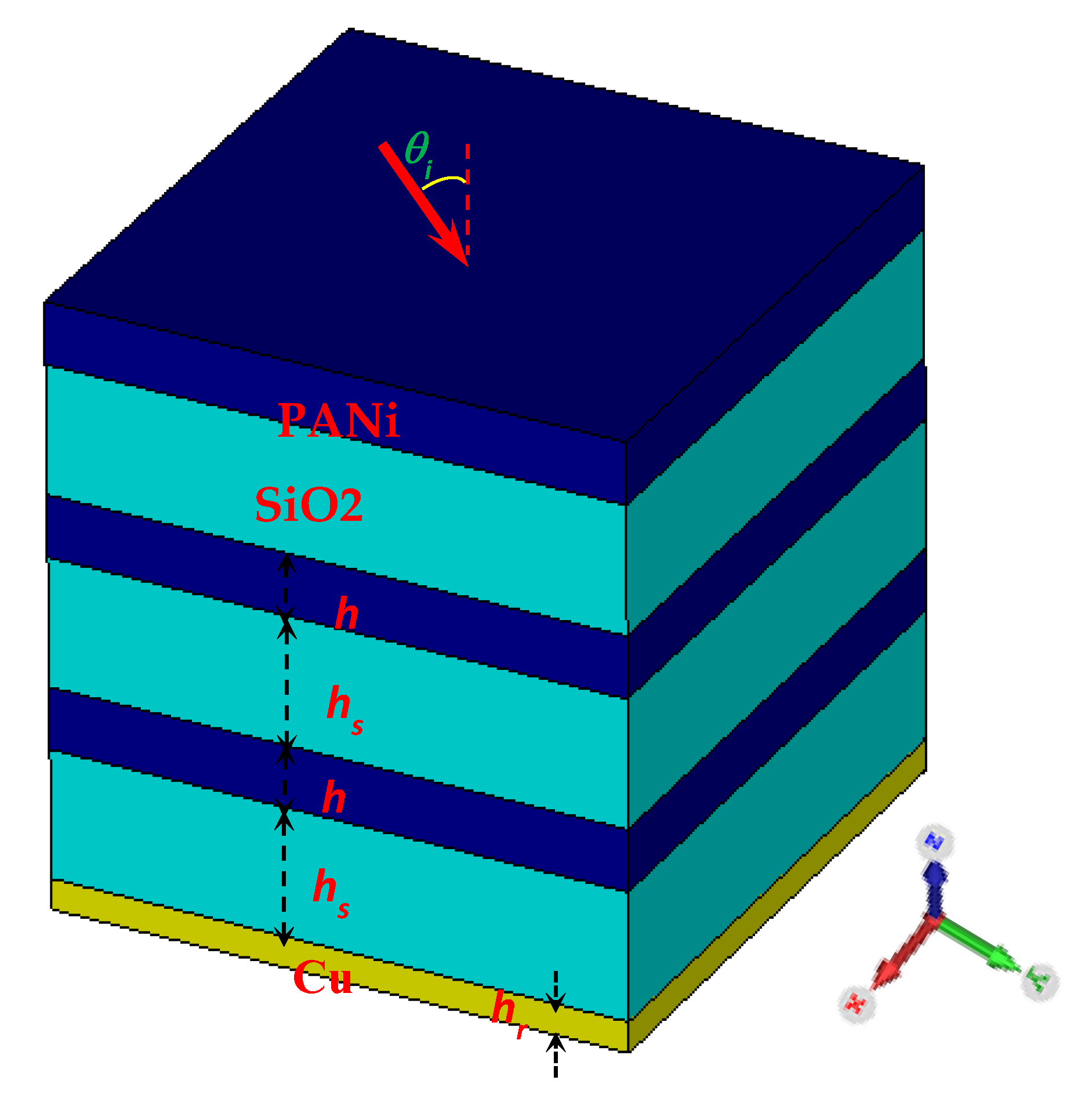
The proposed multilayer metamaterial absorber depicted in Figure 1 comprises stacking layers, including a thin copper (Cu) film at the bottom, SiO2, and PANi. It was determined via numerical simulation that specific parameters substantially influence the device’s efficacy. We set the thickness of the bottom reflector (hr) as 0.2 mm to prevent the propagation of the HPM. We also consider the dielectric constant of silicon dioxide as 2.1 and the loss tangent to be 0.001. The absorption spectrum was analyzed concerning PANi layer thickness variations (h) and the thickness of the SiO2 layer (hs) in various scenarios.
In layered structures, the purpose of stacking layers is to produce tailored structures to obtain specific electromagnetic responses, such as the enhancement of absorption features of the structure. The formation of resonant structures through the stacking of layers enables the manipulation of electromagnetic radiation, thereby facilitating high absorption [36]. Regarding this matter, we construct layered structures composed of PANi and SiO2 with precise geometric parameters to maintain consistent phase differences for electric field components. Stacking a mixture of six layers from PANi and SiO2 results in high coupling between the structure layers, improving performance and UWB absorption.
To design and investigate the suggested HPM absorber, we apply the finite integration approach (FIT), which is implemented in the CST microwave studio. The computation is carried out by utilizing 20 cells per wavelength and introducing adaptive meshing into the computational process. It is necessary to make numerous modifications to the meshes in order to guarantee that the simulation results will be consistent. We apply the unit cell boundary conditions in both directions (X and Y). Also, in the same instant, we set perfectly matched boundary conditions in the Z direction, which is the propagation of the incident HPM. Furthermore, we use Cu as a perfect bottom reflector layer to block the transmission of the waves, considering a thickness greater than the HPM’s skin depth. As a result, the transmission coefficients (T(ω)) can be considered as vanishing. Consequently, the absorption characteristic () for the incident waves of both TE- and TM-polarization can be determined by substituting , where represents the device reflection. Additionally, the absorption characteristic can be calculated utilizing the scattering (S-) parameters: , where represents the reflected waves by the device.
We now demonstrate the complex permittivity of the conductive polymer (PANi) under consideration, as documented in reference [29], within the frequency range of 1–20 GHz. The data for the PANi permittivity calculated in reference [29] pertain to the frequency range of 4–18 GHz. In order to render the dielectric dispersion values for the lower and higher frequencies (specifically, 1–4 GHz and 8–20 GHz) as well, the nth-order dielectric dispersive fitting tool implemented in CST MWS was utilized to model the dielectric properties of these frequencies, as described in reference [37,38]. The complex permittivity of PANi is plotted in Figure 2; it can be seen that the complex permittivity of PANi is dispersive in the entire frequency range of interest (i.e., 1–20 GHz). The real (Re(ϵ)) and imaginary (Im(ϵ)) components of the complex permittivity of PANi are highly positively valued (i.e., dielectric medium), with the magnitude of both decreasing with an increasing frequency. Also, the Im(ϵ) is approximately a fourth of the value Re(ϵ).
Matching impedance plays an important role in EM absorption. A common phenomenon happens when electromagnetic waves move between media, with some energy reflected and the rest transmitted. To reduce reflection, the characteristic impedance of the reflected medium should match that of the incident medium. Impedance matching makes it hard to achieve optimal performance in an absorber design [39]. The absorber impedance should be close to the characteristic air impedance to achieve near-unity absorption, typically around 377 Ω at the appropriate frequency [40]. The reflected component can be computed under the normal excitation as
Assigning to the impedance of the free space, represents the effective impedance of the absorber in this context. Proper matching of the air impedance ( = 377 Ω) is crucial for minimizing energy reflection from structures and ensuring optimal absorption. The impedances of and must be matched precisely. The normalized can be represented using the S-parameters as [41]
To illustrate, we consider the case of hs = 0.8 mm and h = 0.75 mm; the normalized versus frequency has been plotted in Figure 3. It is observed in the provided figure that approaches 1 from 8 GHz and above, indicating that the absorption at a frequency of 8–20 GHz exceeds 90%. Furthermore, the absorption reaches its maximum near the minimal impedance value and, subsequently, declines as the effective impedance increases. Consequently, to decrease wave reflection ( and, thereby, improve the absorbent spectra, adjustments are made to the geometrical parameters of the proposed HPM devices. Investigating the geometrical parameters that result from altering the thickness of the PANi and SiO2 layers is necessary in the given context to improve HPM absorption.
3. Results and Discussion
An investigation is underway into the HPM absorber’s spectral properties depicted in Figure 1. The absorption band for both the TE- and TM-modes is analyzed, taking into account both normal and angular incident electromagnetic waves. The spectral properties of the HPM absorber are initially examined in the context of TE-polarized excitation.
It is evident from Figure 4a that the HPM absorber demonstrates reduced absorption within the frequency range of 2–8 GHz for hs = 0.8 mm. Aside from that range, absorption exceeds 70% and peaks at over 90% for higher frequencies. It is obvious that an increase in h-values results in a further expansion of absorption towards lower frequencies, while a decrease in h values causes an increase in absorption in the higher frequency band.
In Figure 4b, the outcomes are represented for the condition hs = 1 mm. In order to observe the impact of the SiO2 layer thickness, we shall now consider three various values for the thickness of the PANi layers for different h-values, namely 0.6 mm, 0.65 mm, and 0.7 mm, as determined by the CST MWS parametric analysis’s optimal outcomes. It is evident from Figure 4b that an increase in hs results in a marginal reduction in the values of h, which enhances absorption in the sense of greater absorption. It becomes apparent that a reduction in h is necessary to maintain an equivalent level of performance when hs increases. In Figure 4a,b, the proposed device exhibits minimal absorption in the frequency band of 2–8 GHz, which means that high reflection occurs. In the future, we intend to use deep learning algorithms to investigate how to minimize this reflection and enhance the device’s performance.
The subsequent analysis focuses on the impact of the angle of incidence () on the performance of the HPM absorber. The performance of the proposed HPM absorber is influenced by the angle of incidence, . To show the effect of , the angle of incidence is slightly increased by 5° from 0° to 70°. Figure 5 illustrates the absorption characteristic in the case of the oblique incidence of TE waves.
For the parametric values h = 0.75 mm and hs = 0.8 mm, as depicted in Figure 5a, the absorption characteristics versus the angle of incidence under the excitation of TE waves are illustrated. Based on the data presented in Figure 5a, it can be seen that the spectrum remains stable for ≤ 50°, beyond which the absorption efficacy declines gradually. Figure 5b additionally depicts the absorption properties for the parametric values h = 0.65 mm and hs = 1 mm. Clearly, the absorber remains stable even when subjected to angular incidence, and it is also evident that the absorption of high-frequency information has been enhanced compared to the situation depicted in Figure 5a.
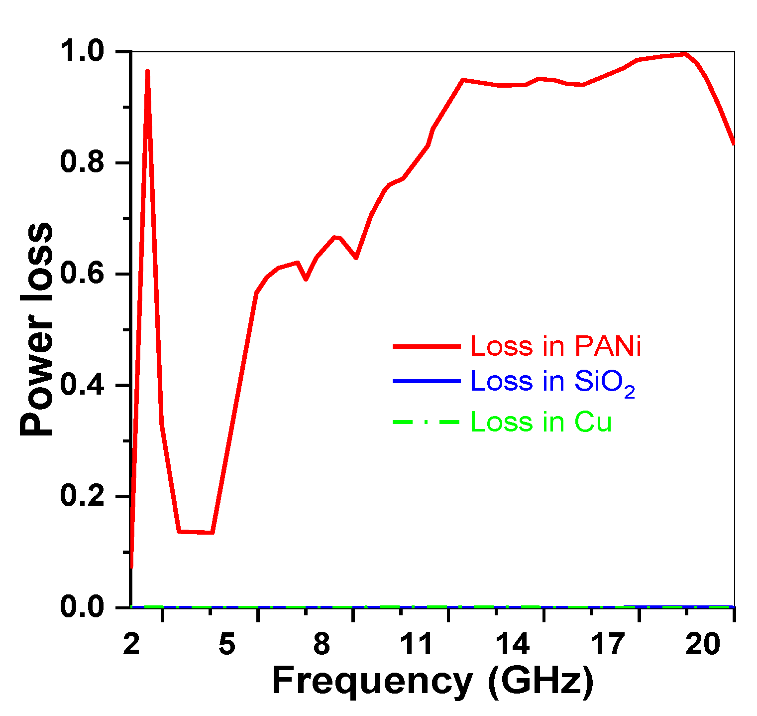
Figure 6 illustrates the normalized power loss experienced by the utilized materials in order to provide insight into the concentration of absorbed power across the various mediums of the HPM absorber. The majority of incident waves are absorbed by the PANi medium of the HPM structure, as observed. Also, it is evident from Figure 6 that SiO2 is a very low-loss material for microwaves due to the low dielectric constant and loss tangent. In order to examine the operational mechanism of the suggested absorbers, the electric field and power density are represented in the XYZ plane. Figure 7 and Figure 8 show the electric field and power density for the proposed HPM structure at h = 0.75 mm and 0.8 mm.
The E-field distribution pattern of the HPM absorber at frequencies of 3 GHz (indicating minimum absorption by the absorber) and 18 GHz (indicating maximal absorption by the absorber) is depicted in Figure 7. As illustrated in Figure 7a, a weak, uniform electric field emanates at a frequency of 3 GHz across all levels. Conversely, when subjected to high absorption at 18 GHz (as illustrated in Figure 7b), the electric field distribution of the device layers differs due to the coupling between the layers of the structure to absorb incident waves to their maximum capacity.
In order to visualize the concentration of absorbed power across each layer of the HPM absorber, the power density for the proposed HPM structure is depicted in Figure 8. It is evident that power losses transpire on the PANi layer of the device for both the 3 GHz and 18 GHz frequencies, as illustrated in Figure 8. The power absorption of the device at 3 GHz is illustrated in Figure 8a. The absorber operates at a modest power level due to a lower amount of absorbed power, which appears on the middle-sandwich layers of PANi. Conversely, the absorber demonstrates maximum absorption across all layers of PANi at 18 GHz.
As a step towards reducing the cost of the developed structure, it is not possible to alter the PANi synthesis process, since we require PANi with a certain complex permittivity. We investigated potential ways to reduce the cost of silicon dioxide, which would, in turn, lower the cost of the developed HPM absorber. Since the cost of silicon dioxide alters depending on the specific dielectric constant, purity, etc., Figure 9a shows the change in the dielectric constant value of SiO2 versus the structure’s absorption. We can see from this figure that the absorption is slightly dependent on the altering of the dielectric constant of SiO2 along the operation band. As a result, we expect to use intrinsic pure silicon dioxide instead of the manufactured one to reduce the cost of the structure.
To overcome the environmental conditions for the proposed HPM absorber such as humidity, UV radiation, etc., we use a coating layer of SiO2 considering two thickness values, namely 0.2 mm and 0.4 mm, as shown in Figure 9b. It can be observed from Figure 9b that the addition of a coating layer made from SiO2 with a thickness of 0.2 mm has almost no impact on the device performance. Also, it is evident from Figure 9a that the small change in the dielectric constant of SiO2 has almost no effect on the absorption spectrum. Consequently, by using SiO2 as a coating layer, we overcome the impact of the environmental conditions on our device because the variation in of the antireflection coating layer due to the environmental conditions can be neglected.
Table 1 provides comparative analyses of the proposed HPM absorber in relation to a number of recent microwave absorber studies. We take into consideration the impact of the following parameters to study the pros and cons of each device in the table, such as absorption efficiency, thickness, material thermal stability, frequency band, angular stability, and device complexity. The observed behavior of the proposed structure under both normal and oblique waves is a broad absorption bandwidth. The substrate material employed in nearly all contemporary structures is FR-4, which is unable to withstand temperatures in excess of 130 °C [42]. Our proposed structure, on the other hand, is composed of materials with high thermal stability, including PANi and SiO2, which qualify it for high-power microwave absorption. The prospective manufacturing process for our HP absorber is relatively uncomplicated, cost-effective, and compatible with layer-by-layer deposition. In addition, the structure possesses a smooth surface, is exceedingly compact and lightweight, and is exceptionally stable in the face of challenging environmental conditions.
4. Conclusions
This study demonstrated an ultra-wideband multilayered metamaterial absorber that shows great promise for absorbing strong electromagnetic waves. Our structure is capable of absorbing high-power microwaves (HPM), since it is composed of silicon dioxide (SiO2) and polyaniline (PANi). To overcome the impact of environmental conditions on the proposed device, we added a 0.2 mm thick SiO2 coating layer. The investigations found that the use of SiO2 as a coating layer will protect the device from environmental conditions and will not affect its performance. Also, prospective fabrication techniques were proposed, and the use of SiO2 with a relative permittivity altering from 2 to 3.6 led to a small impact on the device’s performance. It is expected to withstand up to 400 °C, owing to the use of materials that have high thermal stability, as well as rigorous environmental conditions. By conducting a detailed electromagnetic behavior study, we have shown that our structure significantly improves the absorption bandwidth over the 1–20 GHz frequency range while being stable under normal and oblique transverse electromagnetic wave incidences. In addition to this, our suggested absorber outperforms previous devices in terms of angular incidence stability, surface roughness, and bandwidth, making it an excellent choice for a wide range of applications, including both military and commercial.
Author Contributions
Conceptualization, E.M.S.; methodology, E.M.S.; software, E.M.S.; validation, E.M.S. and A.T.S.; formal analysis, E.M.S.; investigation, E.M.S.; resources, A.T.S.; data curation, E.M.S. and A.T.S.; writing—original draft preparation, E.M.S.; writing—review and editing, E.M.S. and A.T.S.; visualization, E.M.S. and A.T.S.; supervision, A.T.S.; project administration, A.T.S.; funding acquisition, A.T.S. All authors have read and agreed to the published version of the manuscript.
Funding
This research was supported by the Defence Science and Technology Group of the Department of Defence the Commonwealth of Australia (Project ID 10731).
Data Availability Statement
The data introduced in this work are available on request from the corresponding author.
Conflicts of Interest
The authors declare no conflicts of interest.
References
- Min, S.H.; Jung, H.; Kwon, O.; Sattorov, M.; Kim, S.; Park, S.H.; Hong, D.; Kim, S.; Park, C.; Hong, B.H.; et al. Analysis of Electromagnetic Pulse Effects under High-Power Microwave Sources. IEEE Access 2021, 9, 136775–136791. [Google Scholar] [CrossRef]
- Selvaraj, J.; Ware, D.; Dayanikli, G.Y.; Gerdes, R.M.; Gaunkar, N.P.; Mina, M. Electromagnetic induction attacks against embedded systems. In Proceedings of the ASIACCS 2018—ACM Asia Conference on Computer and Communications Security, Incheon, Republic of Korea, 4 June 2018; pp. 499–510. [Google Scholar] [CrossRef]
- Li, F.; Chai, C.; Wu, H.; Wang, L.; Liang, Q.; An, Q.; Yang, Y. Study on high power microwave nonlinear effects and degradation characteristics of C-band low noise amplifier. Microelectron. Reliab. 2022, 128, 114427. [Google Scholar] [CrossRef]
- Giri, D.V.; Sabath, F.; Hoad, R. High-Power Electromagnetic Effects on Electronic Systems; Artech House: Norwood, MA, USA, 2020. [Google Scholar]
- Mumtaz, S.; Rana, J.N.; Choi, E.H.; Han, I. Microwave Radiation and the Brain: Mechanisms, Current Status, and Future Prospects. Int. J. Mol. Sci. 2022, 23, 9288. [Google Scholar] [CrossRef]
- Zhao, M.; Chen, Y.; Zhou, X.; Zhang, D.; Nie, Y. Investigation on Falling and Damage Mechanisms of UAV Illuminated by HPM Pulses. IEEE Trans. Electromagn. Compat. 2022, 64, 1412–1422. [Google Scholar] [CrossRef]
- Brauer, F.; Sabath, F.; Haseborg, J.L.T. Susceptibility of IT network systems to interferences by HPEM. In Proceedings of the 2009 IEEE International Symposium on Electromagnetic Compatibility, Austin, TX, USA, 17–21 August 2009; pp. 237–242. [Google Scholar] [CrossRef]
- Yu, X.H.; Chai, C.C.; Liu, Y.; Yang, Y.T.; Xi, X.W. Simulation and experimental study of high power microwave damage effect on AlGaAs/InGaAs pseudomorphic high electron mobility transistor. Chin. Phys. B 2015, 24, 048502. [Google Scholar] [CrossRef]
- Zhang, D.; Zhou, X.; Cheng, E.; Wan, H.; Chen, Y. Investigation on Effects of HPM Pulse on UAV’s Datalink. IEEE Trans. Electromagn. Compat. 2020, 62, 829–839. [Google Scholar] [CrossRef]
- Haydon, S. Designing and understanding a PCB trace used to deliver EMI to a CMOS microchip using a GTEM. In Proceedings of the 2023 24th International Conference on Applied Electromagnetics and Communications (ICECOM), Dubrovnik, Croatia, 27–29 September 2023; pp. 1–6. [Google Scholar] [CrossRef]
- Sayler, K. Department of Defense Directed Energy Weapons: Background and Issues for Congress; Congressional Research Service: Norwood, MA, USA, 2022.
- Ma, Z.Y.; Chai, C.C.; Ren, X.R.; Yang, Y.T.; Chen, B.; Zhao, Y.B. Effects of microwave pulse-width damage on a bipolar transistor. Chin. Phys. B 2012, 21, 058502. [Google Scholar] [CrossRef]
- Wanasinghe, D.; Aslani, F.; Ma, G.; Habibi, D. Advancements in electromagnetic interference shielding cementitious composites. Constr. Build. Mater. 2020, 231, 117116. [Google Scholar] [CrossRef]
- Miligy, A.F.; Madany, Y.M.; Soliman, A.M. Investigation and Design of Microwave Receiver Protector for Meteorological Radar Applications. In Proceedings of the 2021 International Telecommunications Conference (ITC-Egypt), Alexandria, Egypt, 13–15 July 2021; pp. 1–5. [Google Scholar] [CrossRef]
- Xiong, H. Design of Energy-Selective Surface with an Ultra-wide Shielding Band for High-Power Microwave Protection. ACS Appl. Electron. Mater. 2024, 6, 696–701. [Google Scholar] [CrossRef]
- Sun, Z.; Yan, L.; Zhao, X.; Gao, R.X.K. An Ultrawideband Frequency Selective Surface Absorber with High Polarization-Independent Angular Stability. IEEE Antennas Wirel. Propag. Lett. 2023, 22, 789–793. [Google Scholar] [CrossRef]
- Absorber, A.U.; Absorption, M. An Ultra-Wideband Absorber Based on Mixed Absorption Mechanisms. IEEE Trans. Antennas Propag. 2023, 71, 10009–10013. [Google Scholar] [CrossRef]
- Shukoor, M.A.; Dey, S. Wideband Reconfigurable Multifunctional Absorber/Reflector with Bandpass/Bandstop Filtering and Band-Notch Absorption for. IEEE Trans. Electromagn. Compat. 2024, 66, 153–160. [Google Scholar] [CrossRef]
- Green, M.; Chen, X. Recent progress of nanomaterials for microwave absorption. J. Mater. 2019, 5, 503–541. [Google Scholar] [CrossRef]
- Kumar, A.; Reddy, G.S.; Jyotibhusan, P. Highly Angular-Stable Optically Transparent Microwave Absorber with Wide Absorption Bandwidth. IEEE Lett. Electromagn. Compat. Pract. Appl. 2022, 4, 114–119. [Google Scholar] [CrossRef]
- Hong, Z.; Yu, X.; Xing, Y.; Xue, M.; Luo, Y.; Yin, Z.; Xie, C.; Yang, Y.; Ren, Z. Tunable Head-Conducting Microwave-Absorbing Multifunctional Composites with Excellent Microwave Absorption, Thermal Conductivity and Mechanical Properties. J. Compos. Sci. 2023, 7, 15. [Google Scholar] [CrossRef]
- Govindarajan, G.; Nabi, G.; Mohammed, A.; Savarimuthu, K.; Veeraselvam, A. Miniaturized electromagnetic absorber for millimeter—Wave RADAR systems. Appl. Phys. A 2023, 129, 577. [Google Scholar] [CrossRef]
- Berka, M.; Özkaya, U.; Islam, T.; El, M. A miniaturized folded square split ring resonator cell based dual band polarization insensitive metamaterial absorber for C- and Ku- band applications. Opt. Quantum Electron. 2023, 55, 699. [Google Scholar] [CrossRef]
- Elmahaishi, M.F.; Ismail, I.; Muhammad, F.D. A review on electromagnetic microwave absorption properties: Their materials and performance. J. Mater. Res. Technol. 2022, 20, 2188–2220. [Google Scholar] [CrossRef]
- Mishra, R.R.; Sharma, A.K. Microwave–material interaction phenomena: Heating mechanisms, challenges and opportunities in material processing. Compos. Part A Appl. Sci. Manuf. 2016, 81, 78–97. [Google Scholar] [CrossRef]
- Yang, J.; Liu, X.; Gong, W.; Wang, T.; Wang, X.; Gong, R. Temperature-insensitive and enhanced microwave absorption of TiB2/Al2O3/MgAl2O4 composites: Design, fabrication, and characterization. J. Alloys Compd. 2022, 894, 162144. [Google Scholar] [CrossRef]
- Jia, Z.; Lin, K.; Wu, G.; Xing, H.; Wu, H. Recent progresses of high-temperature microwave-absorbing materials. Nano 2018, 13, 1830005. [Google Scholar] [CrossRef]
- Wang, J.; Sun, Q.; Li, J.; Guo, Y.; Tian, W.; Liu, Y.; Wu, B.; Deng, L.; Mahmood, N.; Jian, X. Polymer-based nanocomposites: Role of interface for effective microwave absorption. Mater. Today Phys. 2023, 31, 100981. [Google Scholar] [CrossRef]
- Chandrasekhar, P.; Naishadham, K. Broadband microwave absorption and shielding properties of a poly(aniline). Synth. Met. 1999, 105, 115–120. [Google Scholar] [CrossRef]
- Wen, M.; Zhao, Y.; Li, Z.; Lai, S.; Zeng, Q.; Liu, C.; Liu, Y. Preparation of lignin-based carbon/polyaniline composites for advanced microwave absorber. Diam. Relat. Mater. 2021, 111, 108219. [Google Scholar] [CrossRef]
- Kulkarni, V.G.; Campbell, L.D.; Mathew, W.R. Thermal stability of polyaniline. Synth. Met. 1989, 30, 321–325. [Google Scholar] [CrossRef]
- Ding, F.; Cui, Y.; Ge, X.; Jin, Y.; He, S. Ultra-broadband microwave metamaterial absorber. Appl. Phys. Lett. 2012, 100, 103506. [Google Scholar] [CrossRef]
- Qu, S.; Hou, Y.; Sheng, P. Conceptual-based design of an ultrabroadband microwave metamaterial absorber. Proc. Natl. Acad. Sci. USA 2021, 118, e2110490118. [Google Scholar] [CrossRef] [PubMed]
- Almoneef, T.S.; Saeed, S.M.; Aldhaeebi, M.A.; Bait-Suwailam, M.M. Wideband metasurface for microwave energy harvesting. In Proceedings of the 2019 IEEE International Symposium on Antennas and Propagation and USNC-URSI Radio Science Meeting, Atlanta, GA, USA, 7–12 July 2019; pp. 1165–1166. [Google Scholar] [CrossRef]
- Feng, T.; Zhu, L. Designs of 3-D Microwave Absorbers with Synthesizable Absorptive Performances. IEEE Trans. Electromagn. Compat. 2024, 66, 80–87. [Google Scholar] [CrossRef]
- Zhang, Z.; Gong, Y.; Pang, K. Optimization and design on multi-layers of dielectric metasurface as broadband terahertz quarter wave plate. J. Opt. 2022, 24, 105101. [Google Scholar] [CrossRef]
- Hosseinbeig, A. Characterization of Relative Complex Permittivity and Permeability for Magneto-Dielectric Sheets. IEEE Trans. Electromagn. Compat. 2018, 60, 1786–1794. [Google Scholar] [CrossRef]
- Ansari, M.A.H.; Jha, A.K.; Akhter, Z.; Akhtar, M.J. Multi-Band RF Planar Sensor Using Complementary Split Ring Resonator for Testing of Dielectric Materials. IEEE Sens. J. 2018, 18, 6596–6606. [Google Scholar] [CrossRef]
- Abdulkarim, Y.I.; Mohanty, A.; Acharya, O.P.; Appasani, B. A Review on Metamaterial Absorbers: Microwave to Optical. Front. Phys. 2022, 10, 893791. [Google Scholar] [CrossRef]
- Sheta, E.M.; Choudhury, P.K.; Ibrahim, A.M.A. Polarization-insensitive ultra-wideband metamaterial absorber comprising different forms of ZrN structures at the metasurface. Opt. Mater. 2022, 133, 112990. [Google Scholar] [CrossRef]
- Sheta, E.M.; Choudhury, P.K. Vanadium nitride-based ultra-wideband nearly perfect metamaterial absorber. J. Nanophotonics 2021, 15, 036007. [Google Scholar] [CrossRef]
- Yuan, J.; Packowski, M.A. The thermal degradation and decomposition of brominated epoxy FR-4 laminates. In Proceedings of the IEEE 43rd Electronic Components and Technology Conference (ECTC ’93), Orlando, FL, USA, 1–4 June 1993; pp. 330–335. [Google Scholar] [CrossRef]
- Shukoor, M.A.; Dey, S.; Koul, S.K. Broadband polarization insensitive wide angular stable dual-split square ring circuit analog absorber for radar cross section and electromagnetic interference shielding applications. Int. J. RF Microw. Comput. Eng. 2022, 32, e23085. [Google Scholar] [CrossRef]
- Liu, S.; Pei, C.; Khan, L.; Wang, H.; Tao, S. Multiobjective Optimization of Coding Metamaterial for Low-Profile and Broadband Microwave Absorber. IEEE Antennas Wirel. Propag. Lett. 2024, 23, 379–383. [Google Scholar] [CrossRef]
Figure 1.
3D schematic of the proposed HPM absorber.

Figure 2.
Relative complex permittivity for PANi.
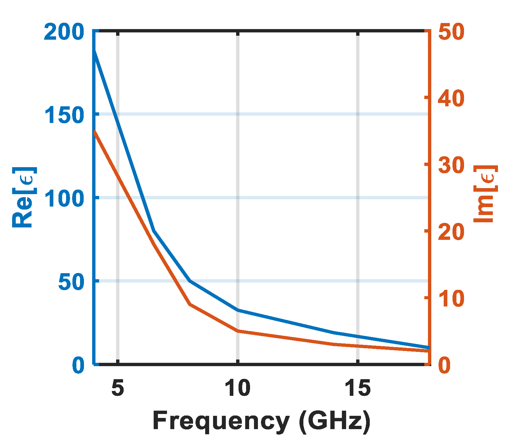
Figure 3.
Frequency dependence of the normalized effective impedance of the HPM absorber.

Figure 4.
Absorption spectrum (A) under various h values for (a) hs = 0.8 mm, (b) hs = 1 mm.
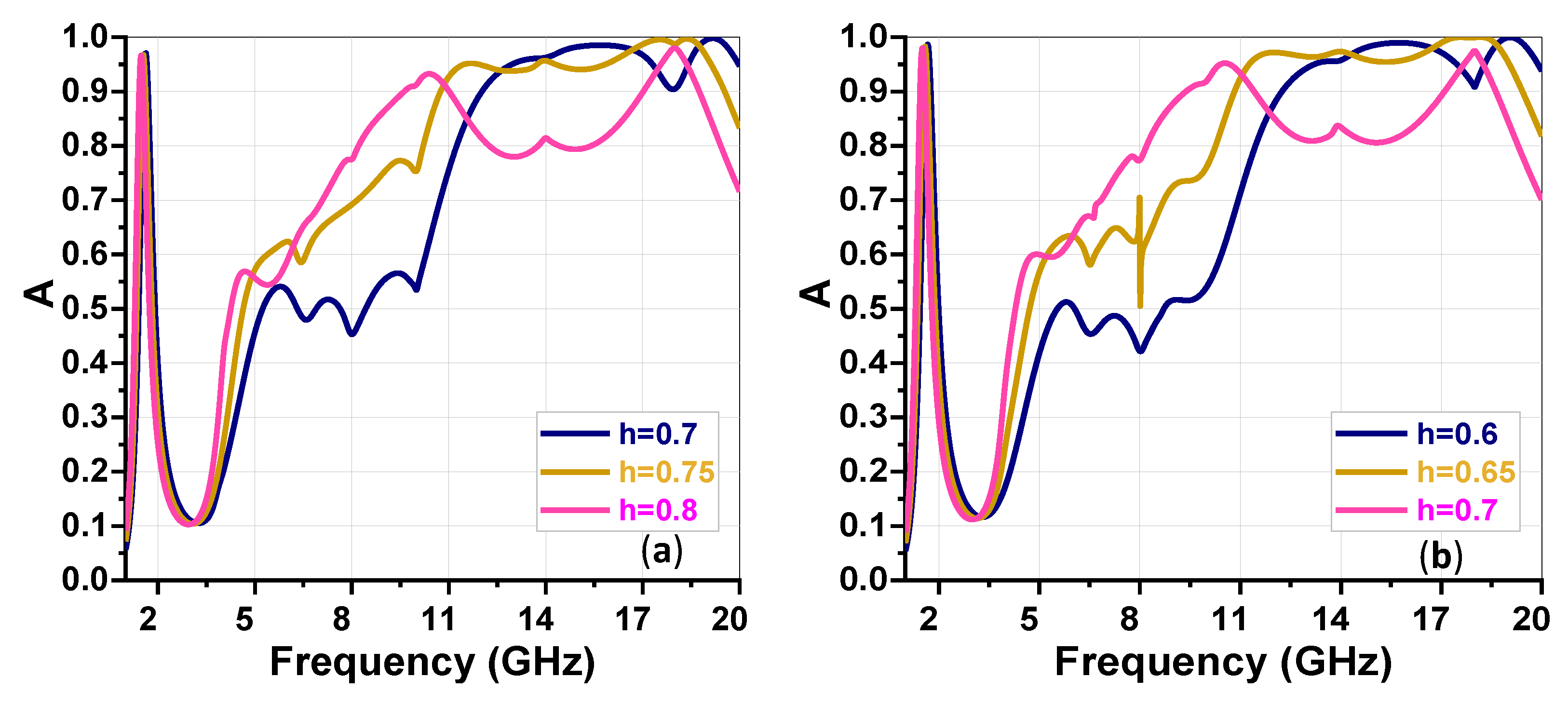
Figure 5.
Absorption spectrum under angular incidence for (a) h = 0.75 mm and hs = 0.8 mm, and (b) h = 0.65 mm and hs = 1 mm.
Figure 5.
Absorption spectrum under angular incidence for (a) h = 0.75 mm and hs = 0.8 mm, and (b) h = 0.65 mm and hs = 1 mm.
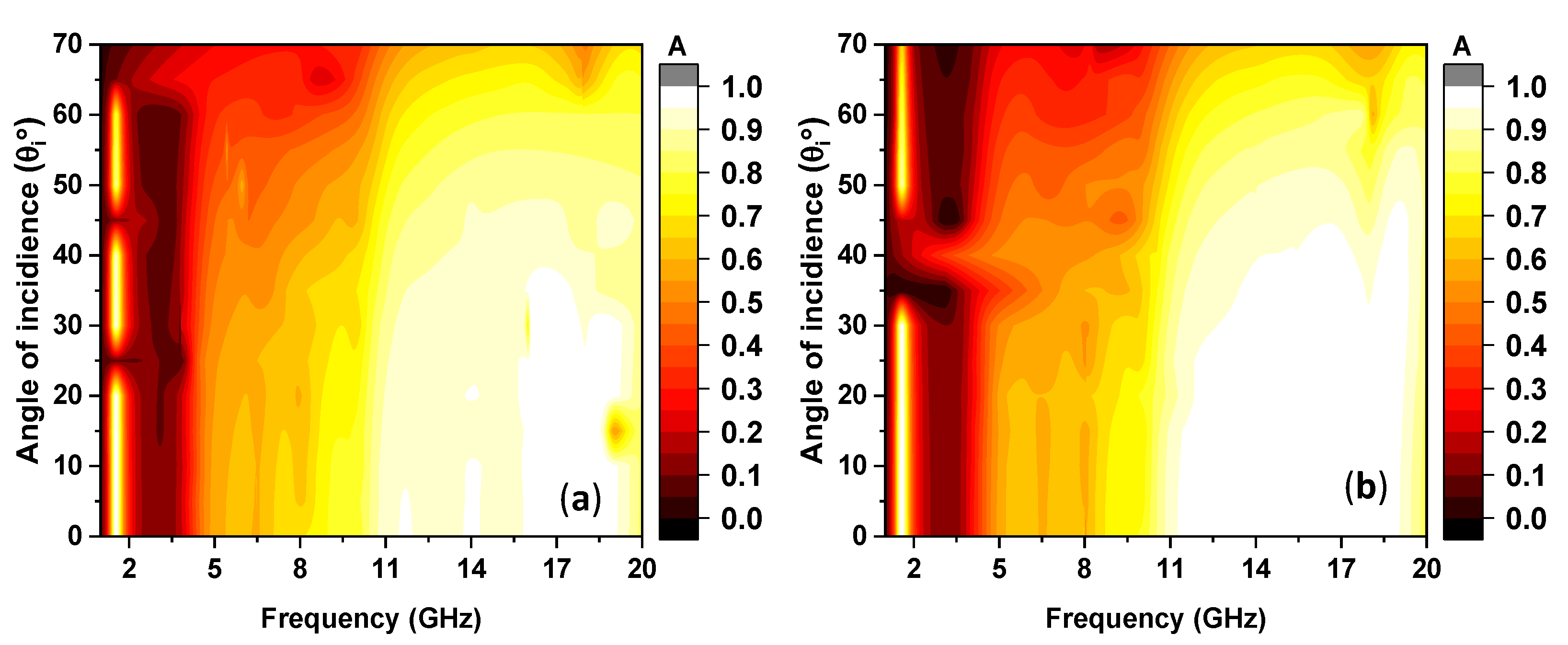
Figure 6.
Plot for power loss (in each material) against frequency considering hs = 0.8 mm and h = 0.75 mm.
Figure 6.
Plot for power loss (in each material) against frequency considering hs = 0.8 mm and h = 0.75 mm.

Figure 7.
3D plot of the electric field at frequencies of (a) 3 GHz and (b) 18 GHz, considering hs = 0.8 mm and h = 0.75 mm.
Figure 7.
3D plot of the electric field at frequencies of (a) 3 GHz and (b) 18 GHz, considering hs = 0.8 mm and h = 0.75 mm.
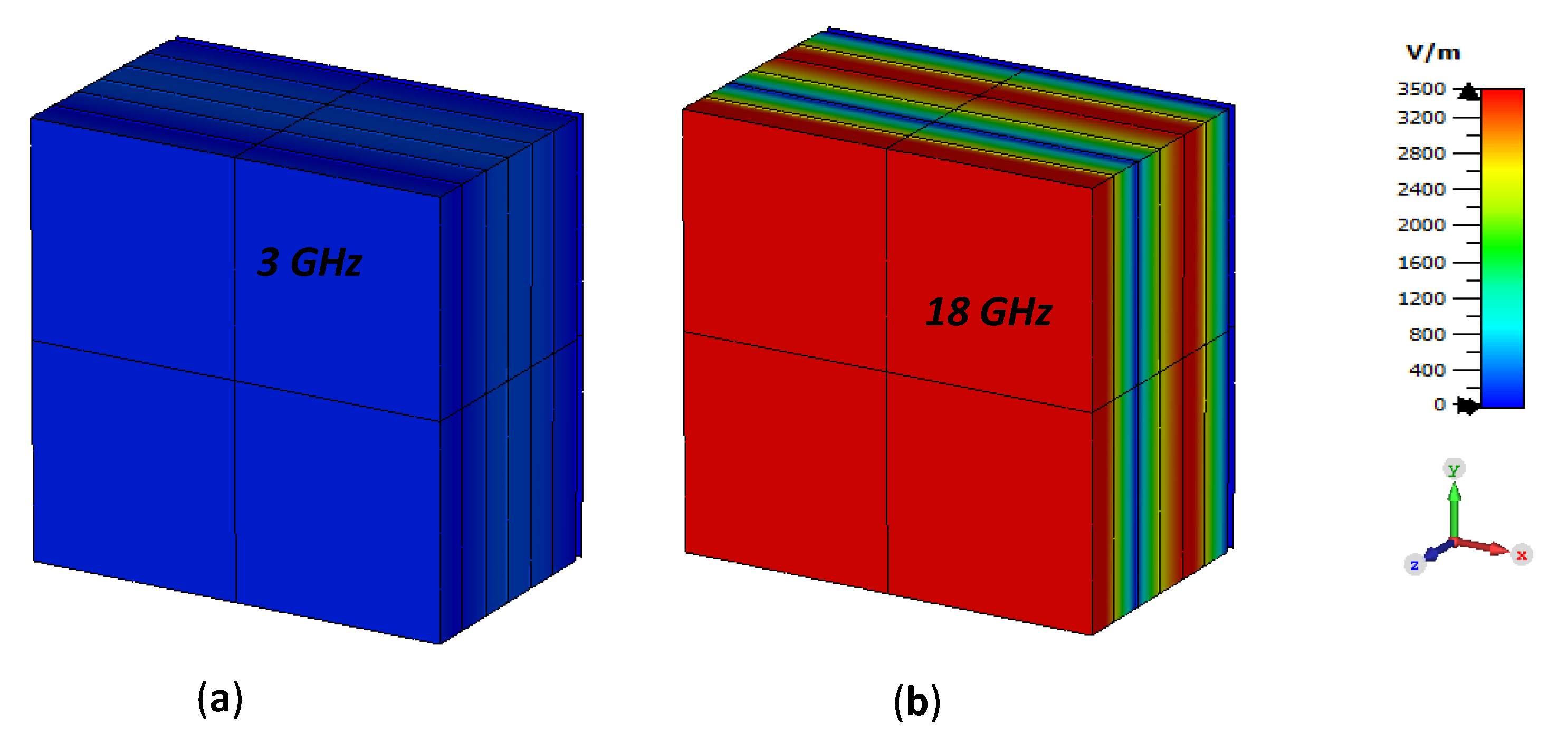
Figure 8.
3D plot of the power loss density at frequencies of (a) 3 GHz and (b) 18 GHz, considering hs = 0.8 mm and h = 0.75 mm.
Figure 8.
3D plot of the power loss density at frequencies of (a) 3 GHz and (b) 18 GHz, considering hs = 0.8 mm and h = 0.75 mm.
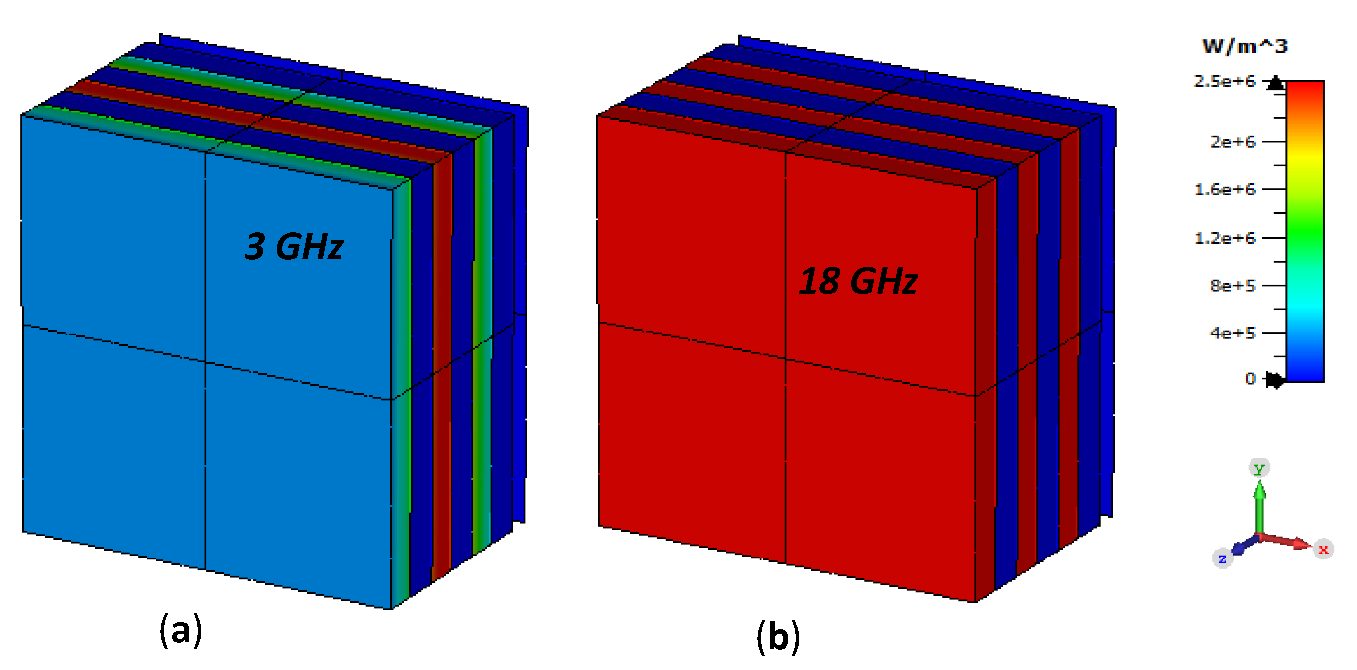
Figure 9.
(a) Absorption spectrum under different various value for dielectric const of SiO2, and (b) absorption spectrum with/without coating layer considering h = 0.75 mm and hs = 0.8 mm.
Figure 9.
(a) Absorption spectrum under different various value for dielectric const of SiO2, and (b) absorption spectrum with/without coating layer considering h = 0.75 mm and hs = 0.8 mm.


Table 1.
Performance comparison of previously reported and proposed layered structures.
| Ref. # | Operating Frequency | Thickness | Angular Stability | Configuration | Investigation | Comments |
|---|---|---|---|---|---|---|
| [23] | 2–16 GHz | 2 mm | θi ≤ 20° | FSS | Full-wave simulation | Selective absorption, Simple structure, unfit for HPM |
| [43] | 6–30 GHz | 4 mm | θi ≤ 45° | Couple of FSS, and air spacer | Simulation and measurement | Simple fabrication, wide bandwidth, unfit for HPM |
| [44] | 7–44 GHz | 4.05 mm | θi ≤ 30° | Coding metamaterial | Simulation and measurement | Complex structure, wide bandwidth, unfit for HPM |
| [20] | 4–16 GHz | 6.5 mm | θi ≤ 50° | FSS and layered materials | Simulation and measurement | Relatively easy fabrication, medium bandwidth, unfit for HPM |
| [18] | 1–8 GHz | 12 mm | θi ≤ 45° | FSS, inductive grid, and two air spacers | Simulation and measurement | Complex structure, less bandwidth, unfit for HPM |
| This work | 1–20 GHz | 5 mm | θi ≤ 50° | Layered structure | Full-wave simulation | Simple structure, ultra-wide bandwidth, suitable for HPM |
Disclaimer/Publisher’s Note: The statements, opinions and data contained in all publications are solely those of the individual author(s) and contributor(s) and not of MDPI and/or the editor(s). MDPI and/or the editor(s) disclaim responsibility for any injury to people or property resulting from any ideas, methods, instructions or products referred to in the content. |
© 2024 by the authors. Licensee MDPI, Basel, Switzerland. This article is an open access article distributed under the terms and conditions of the Creative Commons Attribution (CC BY) license (https://creativecommons.org/licenses/by/4.0/).
Share and Cite
MDPI and ACS Style
Sheta, E.M.; Sutinjo, A.T. Layered Structure Based on PANi and SiO2 to Absorb HPM to Protect Systems and Devices. Crystals 2024, 14, 391. https://doi.org/10.3390/cryst14050391
AMA Style
Sheta EM, Sutinjo AT. Layered Structure Based on PANi and SiO2 to Absorb HPM to Protect Systems and Devices. Crystals. 2024; 14(5):391. https://doi.org/10.3390/cryst14050391
Chicago/Turabian StyleSheta, Essameldin M., and Adrian T. Sutinjo. 2024. "Layered Structure Based on PANi and SiO2 to Absorb HPM to Protect Systems and Devices" Crystals 14, no. 5: 391. https://doi.org/10.3390/cryst14050391
Note that from the first issue of 2016, this journal uses article numbers instead of page numbers. See further details here.