
Designs of Plasmonic Metamasks for Photopatterning Molecular Orientations in Liquid Crystals

 , , and
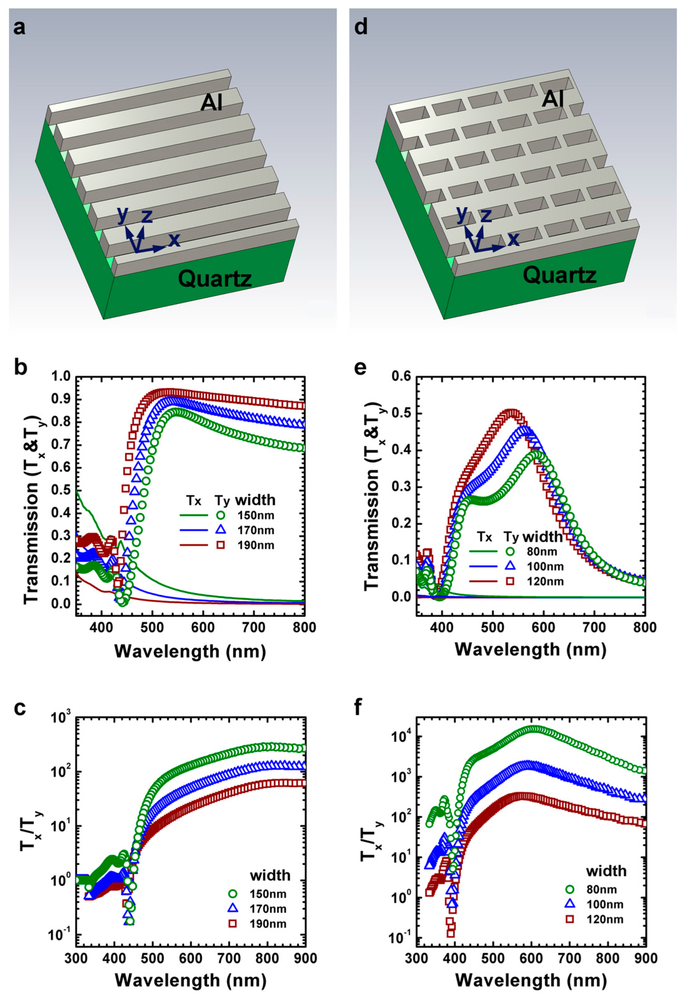
Abstract
:1. Introduction
2. Results
2.1. Design and Simulations of Nanoslit-Based PMMs
2.2. Design and Simulations of Nanoaperture-Based PMMs
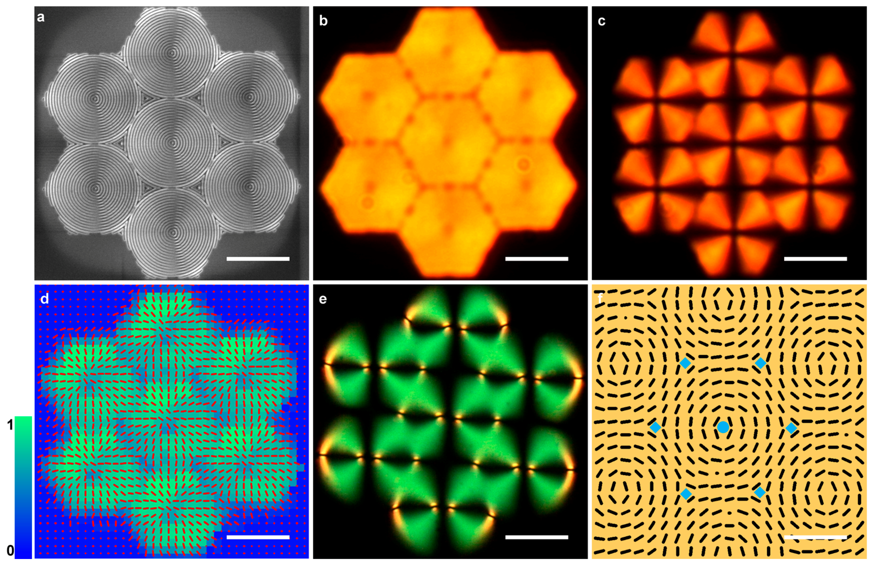
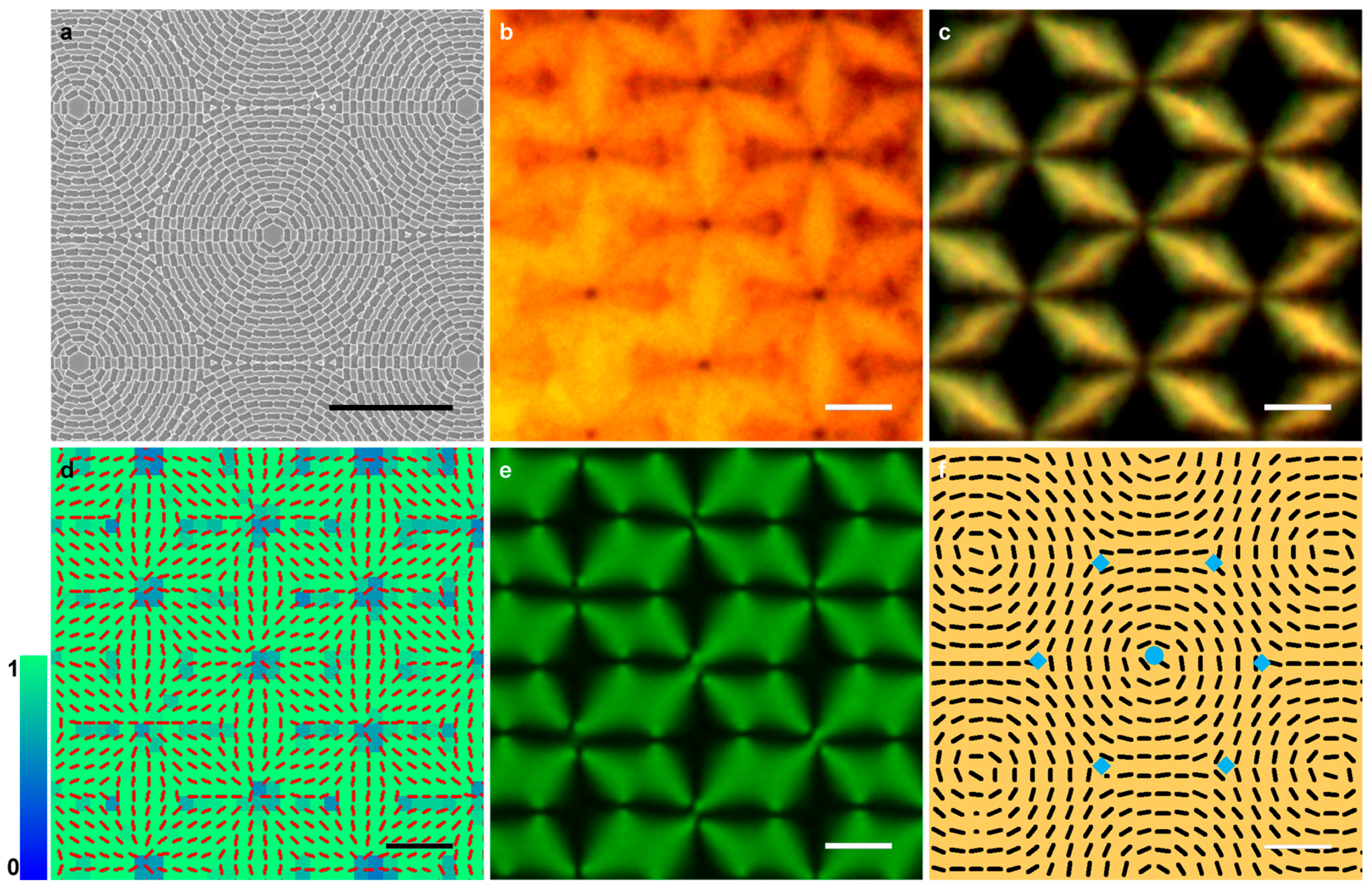
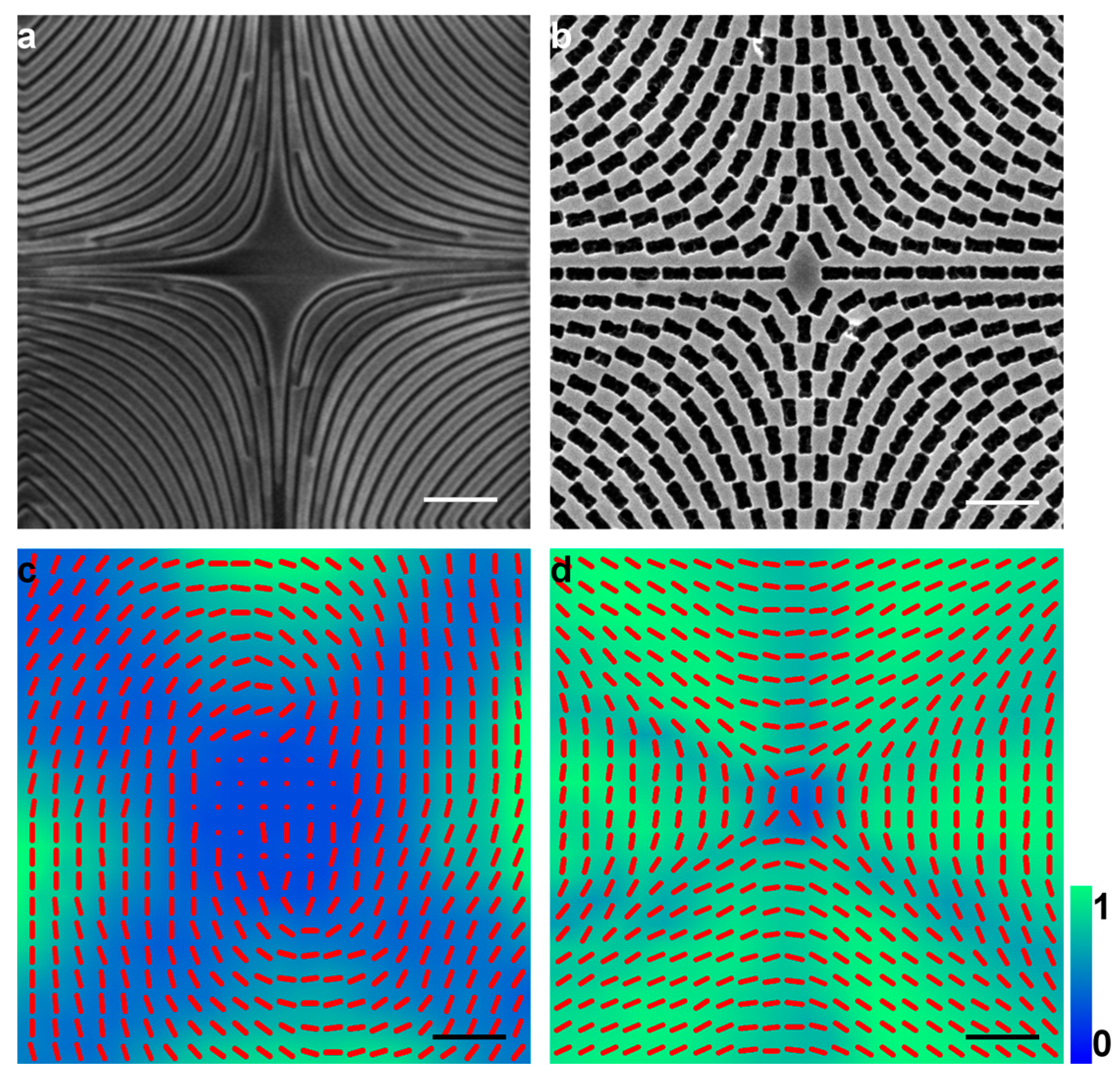
2.3. Photopatterning with Nanoslit-Based PMMs
2.4. Photopatterning with Nanoaperture-Based PMMs
3. Discussion
4. Materials and Methods
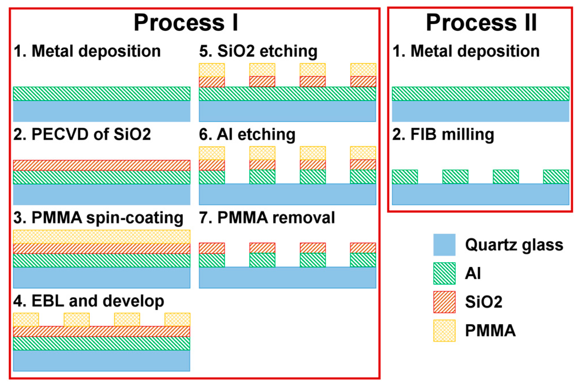
4.1. Fabrication of the PMMs
4.2. Liquid Crystal Cells
5. Conclusions
Acknowledgments
Author Contributions
Conflicts of Interest
References
- McManamon, P.F.; Bos, P.J.; Escuti, M.J.; Heikenfeld, J.; Serati, S.; Xie, H.; Watson, E.A. A Review of Phased Array Steering for Narrow-Band Electrooptical Systems. Proc. IEEE 2009, 97, 1078–1096. [Google Scholar] [CrossRef]
- Beeckman, J.; Neyts, K.; Vanbrabant, P.J.M. Liquid-crystal photonic applications. Opt. Eng. 2011, 50, 081202. [Google Scholar] [CrossRef] [Green Version]
- Marrucci, L.; Manzo, C.; Paparo, D. Optical Spin-to-Orbital Angular Momentum Conversion in Inhomogeneous Anisotropic Media. Phys. Rev. Lett. 2006, 96, 163905. [Google Scholar] [CrossRef] [PubMed]
- Huang, Y.-H.; Ko, S.-W.; Li, M.-S.; Chu, S.-C.; Fuh, A.Y.-G. Modulation of shape and polarization of beam using a liquid crystal q-plate that is fabricated via photo-alignment. Opt. Express 2013, 21, 10954–10961. [Google Scholar] [CrossRef] [PubMed]
- Wei, B.Y.; Hu, W.; Ming, Y.; Xu, F.; Rubin, S.; Wang, J.G.; Chigrinov, V.; Lu, Y.Q. Generating switchable and reconfigurable optical vortices via photopatterning of liquid crystals. Adv. Mater. 2014, 26, 1590–1595. [Google Scholar] [CrossRef] [PubMed]
- Chen, P.; Ji, W.; Wei, B.Y.; Hu, W.; Chigrinov, V.; Lu, Y.Q. Generation of arbitrary vector beams with liquid crystal polarization converters and vector-photoaligned q-plates. Appl. Phys. Lett. 2015, 107, 241102. [Google Scholar] [CrossRef]
- Niv, A.; Biener, G.; Kleiner, V.; Hasman, E. Propagation-invariant vectorial Bessel beams obtained by use of quantized Pancharatnam-Berry phase optical elements. Opt. Lett. 2004, 29, 238–240. [Google Scholar] [CrossRef] [PubMed]
- Gao, K.; Cheng, H.; Bhowmik, A.K.; Bos, P.J. Thin-film Pancharatnam lens with low f-number and high quality. Opt. Express 2015, 23, 26086–26094. [Google Scholar] [CrossRef] [PubMed]
- De Haan, L.T.; Sánchez-Somolinos, C.; Bastiaansen, C.M.W.; Schenning, A.P.H.J.; Broer, D.J. Engineering of complex order and the macroscopic deformation of liquid crystal polymer networks. Angew. Chem. Int. Ed. 2012, 51, 12469–12472. [Google Scholar] [CrossRef] [PubMed]
- Iqbal, D.; Samiullah, M.H. Photo-responsive shape-memory and shape-changing liquid-crystal polymer networks. Materials 2013, 6, 116–142. [Google Scholar] [CrossRef]
- Ware, T.H.; McConney, M.E.; Wie, J.J.; Tondiglia, V.P.; White, T.J. Voxelated liquid crystal elastomers. Science 2015, 347, 982–984. [Google Scholar] [CrossRef] [PubMed]
- White, T.J.; Broer, D.J. Programmable and adaptive mechanics with liquid crystal polymer networks and elastomers. Nat. Mater. 2015, 14, 1087–1098. [Google Scholar] [CrossRef] [PubMed]
- Muševič, I.; Škarabot, M.; Tkalec, U.; Ravnik, M.; Žumer, S. Two-Dimensional Nematic Colloidal Crystals Self-Assembled by Topological Defects. Science 2006, 313, 954–958. [Google Scholar] [CrossRef] [PubMed]
- Peng, C.; Turiv, T.; Guo, Y.; Shiyanovskii, S.V.; Wei, Q.-H.; Lavrentovich, O.D. Control of colloidal placement by modulated molecular orientation in nematic cells. Sci. Adv. 2016, 2, e1600932. [Google Scholar] [CrossRef] [PubMed]
- Kasyanyuk, D.; Pagliusi, P.; Mazzulla, A.; Reshetnyak, V.; Reznikov, Y.; Provenzano, C.; Giocondo, M.; Vasnetsov, M.; Yaroshchuk, O.; Cipparrone, G. Light manipulation of nanoparticles in arrays of topological defects. Sci. Rep. 2016, 6, 20742. [Google Scholar] [CrossRef] [PubMed]
- Peng, C.; Turiv, T.; Zhang, R.; Guo, Y.; Shiyanovskii, S.V.; Wei, Q.-H.; de Pablo, J.; Lavrentovich, O.D. Controlling placement of nonspherical (boomerang) colloids in nematic cells with photopatterned director. J. Phys. Condens. Matter 2017, 29, 014005. [Google Scholar] [CrossRef] [PubMed]
- Lavrentovich, O.D.; Lazo, I.; Pishnyak, O.P. Nonlinear electrophoresis of dielectric and metal spheres in a nematic liquid crystal. Nature 2010, 467, 947–950. [Google Scholar] [CrossRef] [PubMed]
- Peng, C.; Guo, Y.; Conklin, C.; Viñals, J.; Shiyanovskii, S.V.; Wei, Q.-H.; Lavrentovich, O.D. Liquid crystals with patterned molecular orientation as an electrolytic active medium. Phys. Rev. E 2015, 92, 52502. [Google Scholar] [CrossRef] [PubMed]
- Peng, C.; Turiv, T.; Guo, Y.; Wei, Q.-H.; Lavrentovich, O.D. Command of active matter by topological defects and patterns. Science 2016, 354, 882–885. [Google Scholar] [CrossRef] [PubMed]
- McConney, M.E.; Martinez, A.; Tondiglia, V.P.; Lee, K.M.; Langley, D.; Smalyukh, I.I.; White, T.J. Topography from topology: Photoinduced surface features generated in liquid crystal polymer networks. Adv. Mater. 2013, 25, 5880–5885. [Google Scholar] [CrossRef] [PubMed]
- Culbreath, C.; Glazar, N.; Yokoyama, H. Note: Automated maskless micro-multidomain photoalignment. Rev. Sci. Instrum. 2011, 82, 126107. [Google Scholar] [CrossRef] [PubMed]
- Wu, H.; Hu, W.; Hu, H.; Lin, X.; Zhu, G.; Choi, J.-W.; Chigrinov, V.; Lu, Y. Arbitrary photo-patterning in liquid crystal alignments using DMD based lithography system. Opt. Express 2012, 20, 16684–16689. [Google Scholar] [CrossRef]
- Shteyner, E.A.; Srivastava, A.K.; Chigrinov, V.G.; Kwok, H.-S.; Afanasyev, A.D. Submicron-scale liquid crystal photo-alignment. Soft Matter 2013, 9, 5160–5165. [Google Scholar] [CrossRef]
- Du, T.; Fan, F.; Tam, A.M.W.; Sun, J.; Chigrinov, V.G.; Sing Kwok, H. Complex Nanoscale-Ordered Liquid Crystal Polymer Film for High Transmittance Holographic Polarizer. Adv. Mater. 2015, 27, 7191–7195. [Google Scholar] [CrossRef] [PubMed]
- Murray, B.S.; Pelcovits, R.A.; Rosenblatt, C. Creating arbitrary arrays of two-dimensional topological defects. Phys. Rev. E 2014, 90, 52501. [Google Scholar] [CrossRef] [PubMed]
- Van der Asdonk, P.; Hendrikse, H.C.; Fernandez-Castano Romera, M.; Voerman, D.; Ramakers, B.E.I.; Löwik, D.W.P.M.; Sijbesma, R.P.; Kouwer, P.H.J. Patterning of Soft Matter across Multiple Length Scales. Adv. Funct. Mater. 2016, 26, 2609–2616. [Google Scholar] [CrossRef]
- Guo, Y.; Jiang, M.; Peng, C.; Sun, K.; Yaroshchuk, O.; Lavrentovich, O.; Wei, Q.-H. High-Resolution and High-Throughput Plasmonic Photopatterning of Complex Molecular Orientations in Liquid Crystals. Adv. Mater. 2016, 28, 2353–2358. [Google Scholar] [CrossRef] [PubMed]
- Ichimura, K. Photoalignment of liquid-crystal systems. Chem. Rev. 2000, 100, 1847–1873. [Google Scholar] [CrossRef] [PubMed]
- Chigrinov, V.G.; Kozenkov, V.M.; Kwok, H.-S. Photoalignment of Liquid Crystalline Materials: Physics and Applications; John Wiley & Sons Ltd.: Chichester, UK, 2008. [Google Scholar]
- Kawatsuki, N. Photoalignment and Photoinduced Molecular Reorientation of Photosensitive Materials. Chem. Lett. 2011, 40, 548–554. [Google Scholar] [CrossRef]
- Yaroshchuk, O.; Reznikov, Y. Photoalignment of liquid crystals: Basics and current trends. J. Mater. Chem. 2012, 22, 286–300. [Google Scholar] [CrossRef]
- Yu, X.J.; Kwok, H.S. Optical wire-grid polarizers at oblique angles of incidence. J. Appl. Phys. 2003, 93, 4407–4412. [Google Scholar] [CrossRef]
- Liu, X.; Deng, X.; Sciortino, P.; Buonanno, M.; Walters, F.; Varghese, R.; Bacon, J.; Chen, L.; O’Brien, N.; Wang, J.J. Large area, 38 nm half-pitch grating fabrication by using atomic spacer lithography from aluminum wire grids. Nano Lett. 2006, 6, 2723–2727. [Google Scholar] [CrossRef] [PubMed]
- Wang, J.J.; Chen, L.; Liu, X.; Sciortino, P.; Liu, F.; Walters, F.; Deng, X. 30-nm-wide aluminum nanowire grid for ultrahigh contrast and transmittance polarizers made by UV-nanoimprint lithography. Appl. Phys. Lett. 2006, 89, 141105. [Google Scholar] [CrossRef]
- Chen, L.; Wang, J.J.; Walters, F.; Deng, X.; Buonanno, M.; Tai, S.; Liu, X. Large flexible nanowire grid visible polarizer made by nanoimprint lithography. Appl. Phys. Lett. 2007, 90, 063111. [Google Scholar] [CrossRef]
- Wang, J.J.; Walters, F.; Liu, X.; Sciortino, P.; Deng, X. High-performance, large area, deep ultraviolet to infrared polarizers based on 40 nm line/78 nm space nanowire grids. Appl. Phys. Lett. 2007, 90, 061104. [Google Scholar] [CrossRef]
- Wang, F.; Xiao, M.; Sun, K.; Wei, Q.-H. Generation of radially and azimuthally polarized light by optical transmission through concentric circular nanoslits in Ag films. Opt. Express 2010, 18, 63–71. [Google Scholar] [CrossRef] [PubMed]
- Garcia-Vidal, F.J.; Moreno, E.; Porto, J.A.; Martin-Moreno, L. On the transmission of light through a single rectangular hole. Phys. Rev. Lett. 2005, 95, 103901. [Google Scholar] [CrossRef] [PubMed]
- Van der Molen, K.L.; Klein Koerkamp, K.J.; Enoch, S.; Segerink, F.B.; van Hulst, N.F.; Kuipers, L. Role of shape and localized resonances in extraordinary transmission through periodic arrays of subwavelength holes: Experiment and theory. Phys. Rev. B 2005, 72, 45421. [Google Scholar] [CrossRef]
- Kong, F.; Wu, B.-I.; Chen, H.; Kong, J.A. Surface plasmon mode analysis of nanoscale metallic rectangular waveguide. Opt. Express 2007, 15, 12331–12337. [Google Scholar] [CrossRef] [PubMed]
- Garcia-Vidal, F.J.; Martin-Moreno, L.; Ebbesen, T.W.; Kuipers, L. Light passing through subwavelength apertures. Rev. Mod. Phys. 2010, 82, 729–787. [Google Scholar] [CrossRef] [Green Version]
- Mary, A.; Rodrigo, S.; Martín-Moreno, L.; García-Vidal, F. Holey metal films: From extraordinary transmission to negative-index behavior. Phys. Rev. B 2009, 80, 165431. [Google Scholar] [CrossRef]
- Shribak, M.; Oldenbourg, R. Techniques for fast and sensitive measurements of two-dimensional birefringence distributions. Appl. Opt. 2003, 42, 3009–3017. [Google Scholar] [CrossRef] [PubMed]
- Lavrentovich, O.D. Looking at the world through liquid crystal glasses. Contemp. Math. 2011, 577, 25–46. [Google Scholar]
- Yaroshchuk, O.; Gurumurthy, H.; Chigrinov, V.G.; Kwok, H.S.; Hasebe, H.; Takatsu, H. Photoalignment Properties of Brilliant Yellow Dye. In Proceedings of the 14th International Display Workshop, Sapporo, Japan, 5–7 December 2007; pp. 1665–1668.


© 2016 by the authors; licensee MDPI, Basel, Switzerland. This article is an open access article distributed under the terms and conditions of the Creative Commons Attribution (CC-BY) license (http://creativecommons.org/licenses/by/4.0/).
Share and Cite
Guo, Y.; Jiang, M.; Peng, C.; Sun, K.; Yaroshchuk, O.; Lavrentovich, O.D.; Wei, Q.-H. Designs of Plasmonic Metamasks for Photopatterning Molecular Orientations in Liquid Crystals. Crystals 2017, 7, 8. https://doi.org/10.3390/cryst7010008
Guo Y, Jiang M, Peng C, Sun K, Yaroshchuk O, Lavrentovich OD, Wei Q-H. Designs of Plasmonic Metamasks for Photopatterning Molecular Orientations in Liquid Crystals. Crystals. 2017; 7(1):8. https://doi.org/10.3390/cryst7010008
Chicago/Turabian StyleGuo, Yubing, Miao Jiang, Chenhui Peng, Kai Sun, Oleg Yaroshchuk, Oleg D. Lavrentovich, and Qi-Huo Wei. 2017. "Designs of Plasmonic Metamasks for Photopatterning Molecular Orientations in Liquid Crystals" Crystals 7, no. 1: 8. https://doi.org/10.3390/cryst7010008