Review

Status of Growth of Group III-Nitride Heterostructures for Deep Ultraviolet Light-Emitting Diodes

Department of Electrical and Computer Engineering, Virginia Commonwealth University, 601 West Main Street, Richmond, VA 23284, USA
*
Author to whom correspondence should be addressed.
Crystals 2017, 7(10), 300; https://doi.org/10.3390/cryst7100300
Submission received: 4 September 2017 / Revised: 28 September 2017 / Accepted: 29 September 2017 / Published: 4 October 2017
(This article belongs to the Special Issue Advances in GaN Crystals and Their Applications)

Abstract

:
We overview recent progress in growth aspects of group III-nitride heterostructures for deep ultraviolet (DUV) light-emitting diodes (LEDs), with particular emphasis on the growth approaches for attaining high-quality AlN and high Al-molar fraction AlGaN. The discussion commences with the introduction of the current status of group III-nitride DUV LEDs and the remaining challenges. This segues into discussion of LED designs enabling high device performance followed by the review of advances in the methods for the growth of bulk single crystal AlN intended as a native substrate together with a discussion of its UV transparency. It should be stated, however, that due to the high-cost of bulk AlN substrates at the time of writing, the growth of DUV LEDs on foreign substrates such as sapphire still dominates the field. On the deposition front, the heteroepitaxial growth approaches incorporate high-temperature metal organic chemical vapor deposition (MOCVD) and pulsed-flow growth, a variant of MOCVD, with the overarching goal of enhancing adatom surface mobility, and thus epitaxial lateral overgrowth which culminates in minimization the effect of lattice- and thermal-mismatches. This is followed by addressing the benefits of pseudomorphic growth of strained high Al-molar fraction AlGaN on AlN. Finally, methods utilized to enhance both p- and n-type conductivity of high Al-molar fraction AlGaN are reviewed.

1. Introduction

With the excellent properties including compactness, low operating power, and long lifetime, deep ultraviolet (DUV) light-emitting diodes (LEDs) and laser diodes (LDs) with wavelengths in the range of 200–350 nm are of great interests for a wide variety of applications. These include, water and air purification, sterilization/disinfection of medical tools, medical diagnostics, phototherapy, polymer curing, and sensing. Among all the wide bandgap semiconductors, group III-nitrides (GaN, AlN, InN, and their ternary and quaternary alloys) are deemed as the most suitable material family for the implementation of DUV LEDs and LDs. This materials family features a wide tunable emission wavelength range covering the entire UVA (315–400 nm) and UVB (280–315 nm) regions and part of the UVC (100–280 nm) region with the shortest achievable wavelength of 210 nm with this materials system. In addition to the continuously tunable band gap, group III-nitrides also have the advantage of some robust physical properties such as high melting point, high thermal conductivity, high mechanical strength, and most importantly, the possibility of achieving both n- and p-type conduction needed to fabricate a p-n junction diode. During the last decade, a number of groups around the world have been participating in the development of group III-nitrides-based DUV light emitters. Commercial products covering the UVA to UVC range are already available. However, compared with the excellent performance achieved in group III-nitride-based LEDs operating in the near UV and visible ranges, the efficiency of DUV LEDs remains rather modest in that, typical external quantum efficiency (EQE) values of deep UV LEDs are around 0.1%–10%, depending on the wavelength. Many factors have been identified as limiting the implementation of high-efficiency DUV LEDs, encompassing material growth, light extraction, heat dissipation, etc. Almost all aspects of the DUV devices could undergo substantial improvement.
In this review we focus on the most recent progress in growth approaches of group III-nitride heterostructures for DUV LEDs. First, we give an overview of the current status of group III-nitride UDV LEDs and remaining challenges with special emphasis on the limiting factors in the context of material growth. Then, after overviewing DUV device designs for improved efficiency, we segue into discussion of growth and properties of bulk AlN, which is said to eventually provide the platform for the DUV LEDs. Then, approaches for the growth of AlN and high Al-molar fraction AlGaN epilayers are addressed. Finally, methods utilized to enhance both p- and n-type conductivity of high Al-molar fraction AlGaN are discussed.

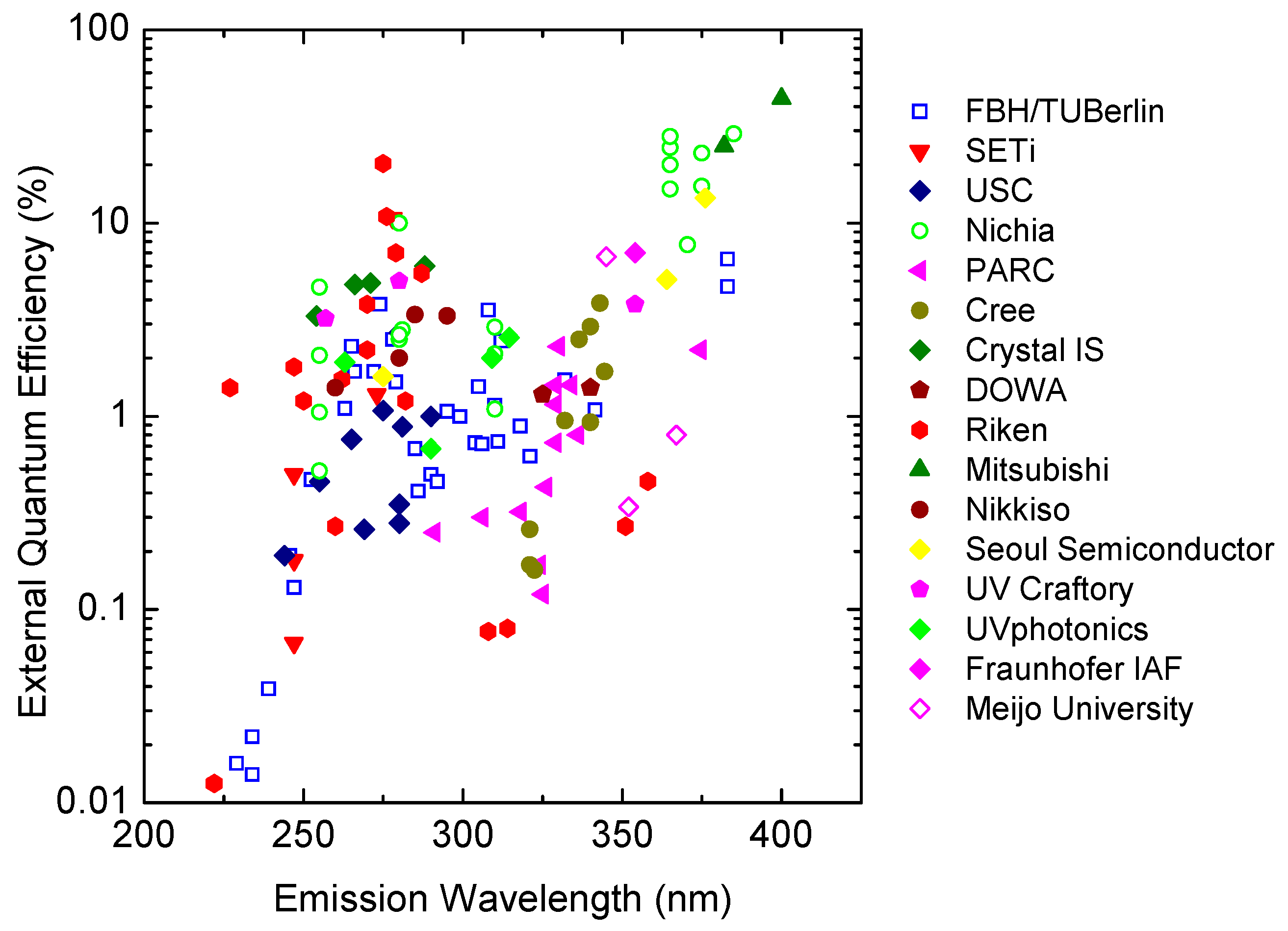
2. Current Status and Challenges of Group III-Nitride DUV LEDs

Benefiting from the improvements in the crystalline quality of AlN and high Al-molar fraction AlGaN layers, and the optimization of LED structure design, the EQE and output power of AlGaN-based DUV LEDs have increased remarkably in recent years. To enumerate, EQE in near and deep UV LEDs with wavelengths between 220 and 400 nm, developed by several industrial and academic groups, is plotted in Figure 1. In 2010, an EQE of over 3% and an output power of over 1 mW at 10 mA continuous wave (CW) driving were demonstrated in flip-chip DUV LEDs with emission wavelengths between 255 and 280 nm [1]. Reasonably high IQE near 70% and an EQE of 1.3% at 100 mA forward current were achieved in 260 nm pseudomorphic UV LEDs on high quality AlN substrates in 2011 [2]. Improvement of the extraction efficiency by die-thinning and encapsulation led to enhancement of the EQE to 4.9% for 271 nm LEDs under CW operation [3]. In 2012, a maximum EQE of 10.4% at 20 mA CW current with an output power up to 9.3 mW for 278 nm DUV LEDs was achieved through migration-enhanced metal organic chemical vapor deposition (MEMOCVD) to reduce the threading dislocation density (TDD) and by using transparent p-type cladding and contact layers, UV reflecting ohmic contacts, and optimized chip encapsulation [4]. In 2015, a 265 nm DUV LED with an output power density above 90 mW/cm2 based on extraction enhancement was reported [5]. In this study, to mitigate the effect of total internal reflection at the AlN surface and the strong absorption of the contact layers, a hybrid structure consisting of photonic crystals and sub-wavelength nanostructures was patterned on the backside of the AlN substrate. A maximum light extraction enhancement of 19.6% was obtained in comparison to that of a flat AlN substrate surface device, resulting in an EQE of 6.3% [5]. To avoid absorption by the p-contact and the p-electrode, researchers replaced p-GaN by transparent p-AlGaN as the p-contact layer, and replaced Ni/Au with Ni(1 nm)/Al as the p-electrode to enhance the reflectivity. In the process, an enhancement of EQE from 2% to 5.5% in 287 nm LEDs grown on sapphire, and a maximum EQE value of 10.8% under 5 mA operating current in 276 nm LEDs were reported [6,7]. In 2017, an EQE of 20.3% under 20 mA direct current was achieved in 275 nm LEDs through enhanced light extraction efficiency (LEE) by using a transparent AlGaN:Mg contact layer, a Rh mirror electrode, an AlN template on a patterned sapphire substrate, and encapsulation resin [8].
As can be seen from Figure 1, despite the unquestionable progress exhibited of late, the EQE of DUV LEDs with emission wavelength below 350 nm is still much lower than those in the near UV range. There are multiple reasons responsible for the reduced performance of DUV devices, including:
(1)
The unavailability of low-cost, lattice, thermal expansion coefficient-matched, and transparent substrate material. Bulk AlN single crystals are very expensive, while sapphire, the most commonly used substrate for DUV LEDs, has a large lattice mismatch (13.3%) and large difference of thermal expansion coefficient with AlN (7.5 × 10⁻⁶ K−1 for sapphire vs. 4.2 × 10⁻⁶ K−1 for AlN), and inferior thermal conductivity.
(2)
The low surface mobility of the Al species on the growth surface, which favors a high density of extended defects such as threading dislocations, resulting in low internal quantum efficiency (IQE) of DUV LEDs.
(3)
The notorious low p-type conductivity in high Al-molar fraction AlGaN due to the large activation energy of Mg acceptor, which results in poor hole injection and also detrimental electron overflow from the active region.
(4)
Low LEE caused by strong total internal reflection and self-absorption.
To conquer the above challenges, many approaches have been proposed and developed for growing better quality group III-nitride heterostructures. In the following, the approaches that have shown advantages/potential for enabling high-EQE DUV LEDs are discussed.

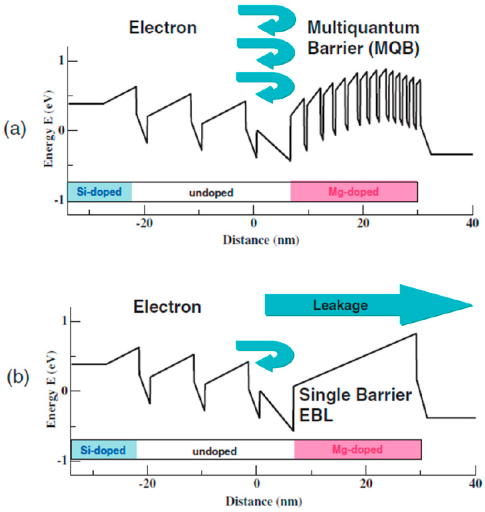
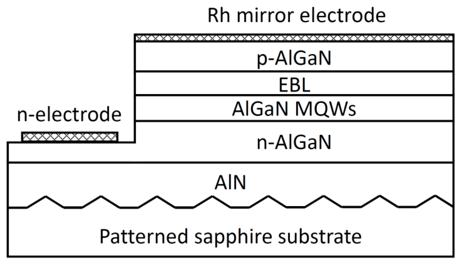
3. Device Design for Improved Performance of Group III-Nitride DUV LEDs

Before discussing challenges, current status, and prospective directions in materials development, we will first focus on the optimization of device design to improve carrier injection efficiency (CIE) and LEE for enhancing the performance of group III-nitride DUV LEDs. To achieve high CIE, an electron blocking layer (EBL) with sufficient high barrier height is required for the suppression of overflow electrons above the multiple quantum wells (MQWs) into the p-type layer. Hirayama et al. [19] reported that the use of a single layer AlGaN EBL with a very high Al-molar fraction of 95% or even AlN is still not sufficient to obtain the desired CIE. To overcome this, the design of AlGaN/AlGaN multiple quantum barriers (MQB) as EBL, which introduces multi-reflection effects, was proposed (see Figure 2). It was found that both the output power and the EQE were significantly increased when a single AlGaN EBL was replaced by the MQB. The EQE of a 250 nm LED was increased by approximately four times to 1.5% by implementing the MQB EBL design. It was estimated that the CIE of the 250 nm LED improved from about 20% to above 80% by using the MQB [20]. Similarly, AlxGa1-xN/Al0.7Ga0.3N electron blocking heterostructures (EBHs) were investigated to enhance the injection efficiency by Kolbe et al. [14] The output power of 290 nm LEDs with an optimized AlN/Al0.7Ga0.3N EBH increased by a factor of around 8.5 compared to LEDs with a conventional Al0.7Ga0.3N EBL.
DUV LEDs generally employ flip-chip configuration for efficient heat dissipation and light extraction [21,22,23,24]. In spite of this, flip-chip designs still suffer from a relatively low extraction efficiency caused by the dominant transverse magnetic (TM)-polarized light emission, which propagates mainly in the lateral direction [25]. Sidewall emission-enhanced (SEE) DUV LEDs with multiple light-emitting mesa stripes and three-dimensional reflectors between the stripes were explored to enhance the light extraction efficiency of TM-polarized light [25,26]. Remarkably enhanced light extraction with a strongly upward-directed emission due to the exposed sidewall of the active region and Al-coated selective-area-grown n-type GaN micro-reflectors was observed in the SEE DUV LEDs with an emission wavelength of 285 nm. The devices also showed reduced operating voltage due to improved n-type ohmic contacts formed on the regrown n-GaN stripes compared with conventional LEDs.
A moth-eye structure was fabricated on the back side of the sapphire substrate for 255–280 nm UVC LEDs reported by Pernot et al., and on-wafer output power measurement revealed a 1.5-fold improvement of light extraction [1]. Ichikawa et al. [27] reported the application of hemispherical sapphire lenses bonded to the substrates of DUV LED chips to enhance the light extraction efficiency. The 255 nm DUV LEDs with a sapphire lens fabricated using the surface activated bonding method showed a light extraction efficiency enhancement of 2.8 times when compared to a reference LED lacking the lens, and an EQE of 4.56% was achieved. Inoue et al. [5,24] developed large-area AlN nanophotonic structures to enhance the light extraction efficiency of DUV LEDs. The LEDs with the nanoimprinted AlN nanophotonic structures exhibited wider near-field emitting areas, stronger far-field extracted light intensities, and an approximately 20-fold increase in the output power when compared with a conventional flat-surface DUV LED. A CW output power in excess of 150 mW for an injection current of 850 mA was achieved in the nanoimprinted UVC LEDs emitting at 265 nm [24].
Nagai et al. [28,29,30] investigated the feasibility of encapsulation of AlGaN-based DUV LEDs with silicone resin and with polymerized perfluoro-4-vinyloxy-1-butene (BVE)-based fluorine polymers having –COOCH3 ends in comparison with fluorine polymers having terminal ends of –CF3 and –COOH in order to enhance light extraction. Serious damage to the electrode metal was observed, except for the BVE-based polymer with –CF3 ends. For DUV LEDs encapsulated with the selected BVE-based polymers with –CF3 ends, a stable 1.5 times light extraction enhancement with no degradation of the fluorine resin over 6000 h at a wavelength of 265 nm was obtained. In addition, a 3 × 4 array module of encapsulated 285 LED dies on a simple AlN submount with an output power of 472 mW at 200 mA and 63 V was achieved with a 1.5 fold light extraction enhancement as well.

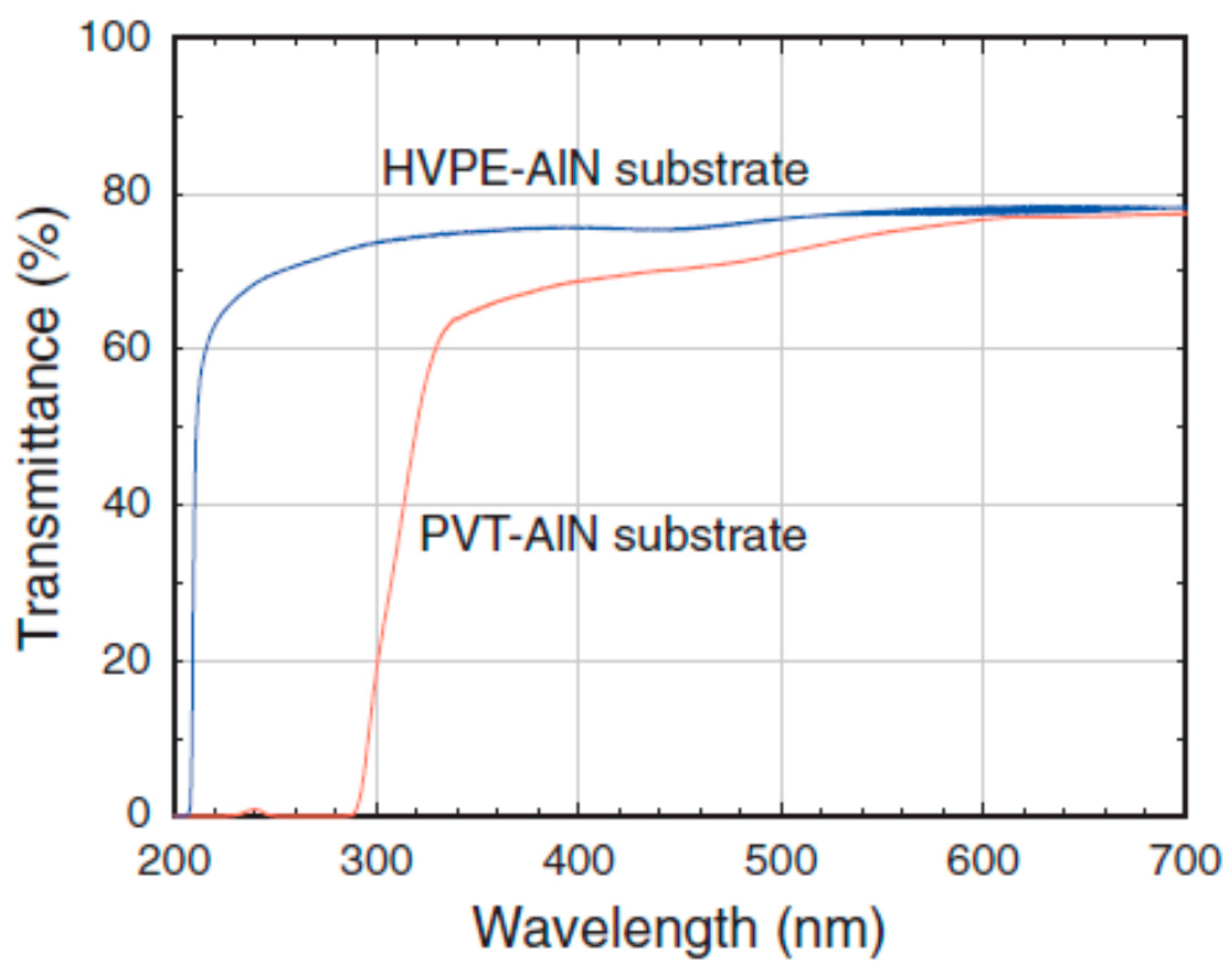
4. Growth and Optical Properties of Bulk AlN for DUV LEDs

Ideal substrates for the growth of AlGaN-based DUV LEDs must possess the physical properties that closely match with the epilayers being grown on them. The requirements include favorable crystal structure (similar symmetry, closely matched lattice constants), similar thermal expansion coefficient, high thermal conductivity, and optical transparency. Table 1 lists the major characteristics of substrates applicable for DUV LEDs. None of the typically used substrates is ideal and fully satisfies all the requirements. Because of silicon’s low cost, large wafer size, high crystalline quality, good electrical conductivity, and feasibility of its removal through chemical etching to allow back light extraction, III-nitride based LEDs grown on silicon substrates have also been extensively studied. However, large lattice and thermal mismatch between III-nitrides and silicon result in tensile strain, leading to high crack and dislocation densities in DUV LED structures. Both 6H-Silicon carbide (SiC) and 4H-SiC exhibit much smaller lattice and thermal misfits with III-nitrides. They also have the advantages of good chemical stability, and high electrical and thermal conductivity, but relatively high cost compared with sapphire and silicon substrates. GaN substrates have a low lattice mismatch with the AlGaN-based heterostructures grown on them (between 0% and 2.4%, depending on Al-molar fraction) and excellent physical properties such as high thermal conductivity and mechanical strength. The main growth methods for bulk GaN, or bulk-like GaN, include hydride vapor phase epitaxy (HVPE) and ammonothermal growth. So far, GaN crystals with diameters from 2 to 4 inch and dislocation densities below 105 cm−2, which is much lower than that in GaN grown on foreign substrates, have been reported for both methods [31,32]. However, for DUV LEDs, GaN has the drawbacks of generation of tensile strain in the AlGaN epilayers with high Al-molar fraction and light absorption and also high-cost. For Si, SiC, and GaN substrates, when and if used, the substrates must be selectively removed during fabrication for DUV LEDs which are back-emitting. Owing to its excellent DUV transparency, low cost and similar crystal symmetry as III-nitrides, today’s efforts in development of DUV LEDs are mainly focused on utilization of sapphire as the substrate despite its shortcomings. Typical threading dislocation density (TDD) of AlGaN heterostructures on sapphire conventionally produced using low-temperature AlN buffer is above 1010 cm−2 due to the large lattice- and thermal-mismatch between AlGaN and sapphire. This is detrimental in that a relatively high IQE of DUV LEDs (above 50%) requires TDD values below 109 cm−2 [13]. We l leave the discussion of the approaches employed for reducing TDD in AlGaN heterostructures on foreign substrates to Section 5, Section 6 and Section 7. In the remainder of this section we focus on the progress made in bulk growth and properties of AlN, which is the most promising substrates for DUV LEDs due to its low lattice mismatch for high Al-molar fraction AlGaN, high breakdown voltage and thermal conductivity, chemical inertness, despite the restrictions imposed by its limited availability, and high cost at the time of this writing.
The most promising technique for the growth of bulk AlN crystals is sublimation-recondensation, also known as the physical vapor transport (PVT) method [35]. The sublimation-recondensation reaction can be written as
2 AlN ( s ) 2 Al ( g ) + N 2 ( g )
In the growth reactor, AlN powder source is sublimated from a crucible with a temperature above 2000 °C under N2 atmosphere. Due to the thermal gradient with an intentionally induced slightly higher source temperature compared to the seed temperature, Al and N atoms transport toward the seed and condense to form an AlN bulk crystal. Although PVT growth of AlN can take place at temperatures below 1800 °C, the material quality is limited by the mobility and reactivity of the atoms; therefore, higher temperatures, around 2200 °C, are more favorable for enhancing both the growth rate and crystal quality. Typically, bulk AlN crystals are grown at temperatures between 1800 °C and 2200 °C, a reactor pressure in the range of 300–900 mbar, and a thermal gradient of 10–50 K/cm, which yield a growth rate around several hundred micrometers per hour. In addition to the precise control of both the seed and source temperature and the purity of the source, the choice of the crucible material is also crucial to the quality and the properties of the resulting AlN crystals [36].
Although there are still challenges, such as contamination from impurities, lack of large-sized AlN seeds, and difficulty in tailoring desired thermal profile inside the growth reactor that hinder reproducible growth to cite a few [37], several groups have achieved PVT-grown AlN single crystals with diameters up to 2 inch [35,38,39,40,41,42]. X-ray rocking curves with a full width at half maximum (FWHM) close to 30 arcsec for both (0002) and (10 1 ¯ 2) reflections and etch pit densities (EPDs) below 104 cm−2 were reported with an usable area of ~85% [35]. Low dislocation density AlGaN epilayers with both symmetric and asymmetric rocking curves below 100 arcsec have been grown on these AlN wafers. Significant improvements in the performances of DUV LEDs have also been demonstrated by the use of PVT-AlN substrates [2,43,44,45]. For instance, an IQE of 80% was reported for AlGaN multiple quantum wells with emission wavelength of 258 nm grown on PVT-AlN substrates, achieved with the reduction of point defects by growth optimization [46].
In addition to crystal quality and size, UV transparency of the AlN substrate is also of crucial importance for applications in DUV LEDs. Although AlN should be transparent down to 210 nm due to its wide bandgap of 6 eV, PVT-AlN substrates have shown wide optical absorption bands below the band gap in the blue and UV ranges [38,47,48]. These absorption bands are attributed to residual impurities such as silicon, oxygen (mainly from the source materials), and carbon (mainly from the reactor parts such as TaC crucible) and intrinsic point defects, and Al vacancies. The underlying mechanisms for the formation of these bands are still under discussion [38,42,47,48,49,50,51,52,53].
Specifically, at least three absorption bands at 2.8 eV, 3.3–4.3 eV, and 4.7 eV were found and discussed for PVT-grown AlN. The origin of the 2.8 eV band is still an issue of intense debate. Some researcher ascribed it to transition between the valence band and Al vacancy (VAl) level [53]. However, others attributed it to transitions between oxygen on N sites (ON) and VAl (ON-VAl) [47]. The broad 3.3–4.3 eV band is presumably associated with VAl and/or oxygen related complexes, and reduction of oxygen contamination in the source material was found to lead to a significant decrease of UV absorption in both colorless and yellowish areas of bulk AlN [47]. The 4.7 eV band with an absorption coefficient above 1000 cm1, which is detrimental to DUV LEDs with emission wavelength shorter than 270 nm, was typically observed in crystals grown with TaC crucibles. To minimize this absorption, the AlN substrates were thinned down to 20 μm [3]. The origin of the 4.7 eV band was reportedly related to carbon contaminations [51]. Density functional theory (DFT) calculations have predicted that substitutional carbon on the nitrogen site (CN) introduces absorption at this energy. Optical absorption measurements performed on a series of single crystalline AlN wafers with different carbon concentrations showed that the absorption coefficient at 4.7 eV linearly increased with carbon content, supporting the prediction of CN being responsible for the said absorption [51].
Another promising method for growing bulk AlN crystals is hydride vapor phase epitaxy (HVPE). Compared to the PVT produced AlN, HVPE grown AlN has much better transparency in the DUV range due to better controlled carbon incorporation. Freestanding AlN substrates prepared by HVPE also showed a steep optical transmission cutoff near the band edge [54]. The disadvantage of the HVPE method is that, it may produce AlN crystals with high TDD and crack densities due to the large lattice and thermal mismatch between AlN and the foreign substrates such as SiC and sapphire, as shown in Table 1. Typical TDD in HVPE AlN on foreign substrates is above 107 cm2. For example, a TDD of 1.5 × 108 cm2 on sapphire [54] and 3 × 109 cm2 on Si (111) [55] were reported.
To avoid cracks and reduce TDD, HVPE growth of AlN using native PVT-AlN substrates has been explored. Although AlN layers grown by low-pressure HVPE on on-axis PVT-AlN (0001) substrates were reported to echibit cracks due to tensile strain, no cracks were found in the structures grown on AlN (0001) substrates with 5° off-cut angle [56]. X-ray ω-rocking curves with FWHM values of 277 and 306 arcsec were achieved for the (0002) and (10 1 ¯ 0) reflections. It was also found that the Si and C impurity concentrations in the overgrown AlN layer reduced to half of those in the PVT-AlN substrates. In another study [57], FWHM values as small as 31 and 32 arcsec were reported for the (0002) and (10 1 ¯ 1) reflections of ω-rocking curves, respectively, for 114 µm-thick HVPE-AlN, grown on a bulk PVT-AlN substrate. The HVPE-AlN has larger external optical transmittance in the DUV range compared to the PVT-AlN substrate, with a steep optical transmission cutoff at 206.5 nm (Figure 3), which was attributed to lower concentrations of carbon, and oxygen impurities, and VAl in the HVPE-AlN substrate.
By using HVPE-AlN as a substrate for growth and subsequent removal of it by mechanical polish, an output power of 28 mW and an EQE of 2.4% were obtained at an injection current of 250 mA in 268 nm DUV LEDs [58]. In another study, TDD in 261 nm DUV LED heterostructures (except the p-GaN layer) grown on HVPE-AlN/PVT-AlN substrates was found to be below 106 cm2 from transmission electron microscopy (TEM) analysis. The lifetime of these LEDs was estimated to be over 10,000 h for CW operation at 50 mA, and over 5000 h for CW operation at 150 mA [9].

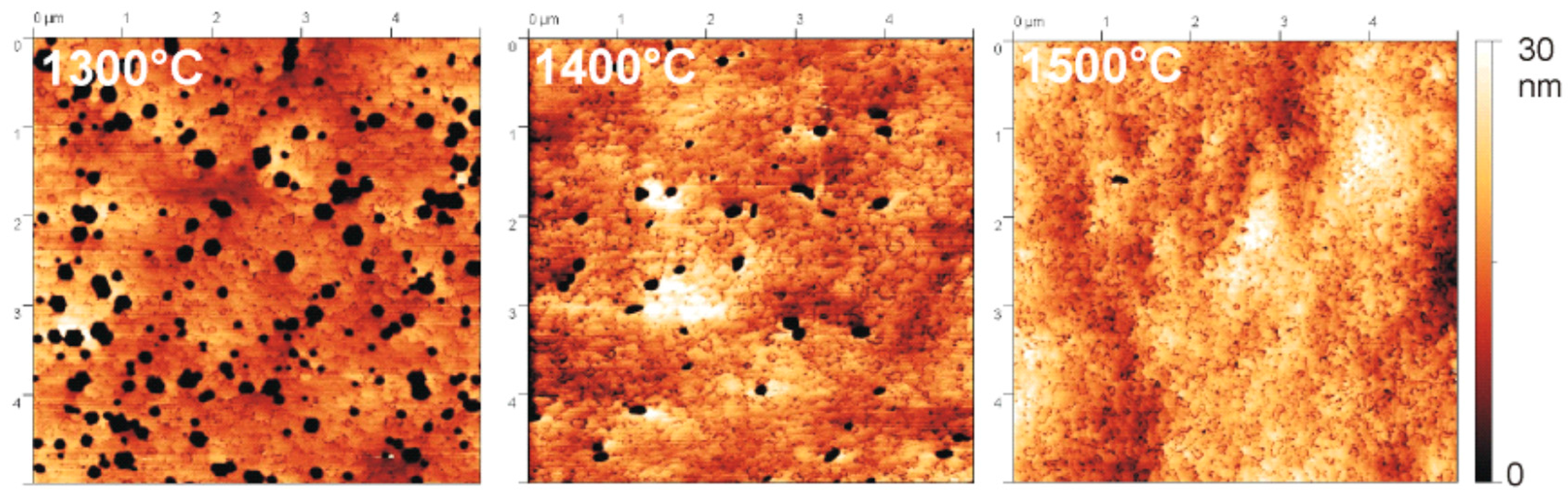
5. High-Temperature Growth of AlN and High Al-Molar Fraction AlGaN by MOCVD

Not only the lattice and thermal mismatch between the epilayer and foreign substrates, but also the low surface adatom mobility of Al at typical growth temperatures (below 1200 °C) is a dominating factor that leads to the generation of high TDD in AlGaN-based DUV LEDs. Due to the lower surface migration rate (mobility) of Al than that of Ga, it is more difficult to achieve the layer-by-layer two-dimensional growth of AlN and high Al-molar fraction AlGaN. At typical growth temperatures (1200 °C or less), Al adatoms cannot move to energetically favorable lattice steps, thus resulting in three-dimensional (3D) islandic growth and the formation of extended defects such as dislocations and grain boundaries. Therefore, the crystalline quality degrades in AlGaN with increasing Al content. Because the surface diffusion coefficient is strongly temperature dependent, and adatom surface mobility increases with increasing growth temperature, high-temperature MOCVD technique has been employed for the growth of AlN and high Al-molar fraction AlGaN.
Figure 4 shows the evolution of surface morphologies of AlN on sapphire substrate grown at different temperatures [59]. When growing AlN at growth temperatures typical of GaN (~1200 °C) the surface showed 3D columnar-like morphology (not shown). At an increased temperature of 1300 °C, transition from the rough morphology to a rather flat surface exhibiting a high density of hexagonal pits was observed. When the temperature was raised further up to 1500 °C, the pit density reduced drastically and a smooth surface with an rms roughness value of 0.4 nm was achieved.
In addition to the reduction of TDD and providing a flat surface morphology, high temperature growth was also found to be effective for reducing the density of unintentional impurities and point defects in AlN and high Al-molar fraction AlGaN, which is critically important for enhancing the IQE of DUV LEDs. Secondary ion mass spectroscopy (SIMS) has shown that, in pit-free AlN layers grown at 1500 °C and above, oxygen and Si concentrations were 5 × 1017 cm−3 and 1 × 1017 cm−3, respectively, while oxygen concentration was above 1 × 1019 cm−3 in samples with a high pit density [59]. Similar results have been reported in another study [60,61]. In AlN films grown at high temperatures (above 1350 °C), they were found to be below the detection limit of SIMS, while for AlN grown below 1200 °C, the Si, C, and O concentrations were of the order of 1018–1019 cm−3. The low temperature (12 K) cathodoluminescence (CL) spectra recorded on high temperature grown AlN films were characterized by sharp excitonic emission peaks with weak broad defect-band emission [62]. In contrast, the CL spectra from samples grown at relatively low temperatures revealed intense defect-band emission with broad near band edge emission. Time-resolved photoluminescence (TRPL) and time-resolved cathodoluminescence (TRCL) measurements for high Al-molar fraction AlGaN films also confirmed that high temperature growth with appropriate defect management is preferable to reduce nonradiative recombination, which is crucial for high IQE in DUV LEDs [61].

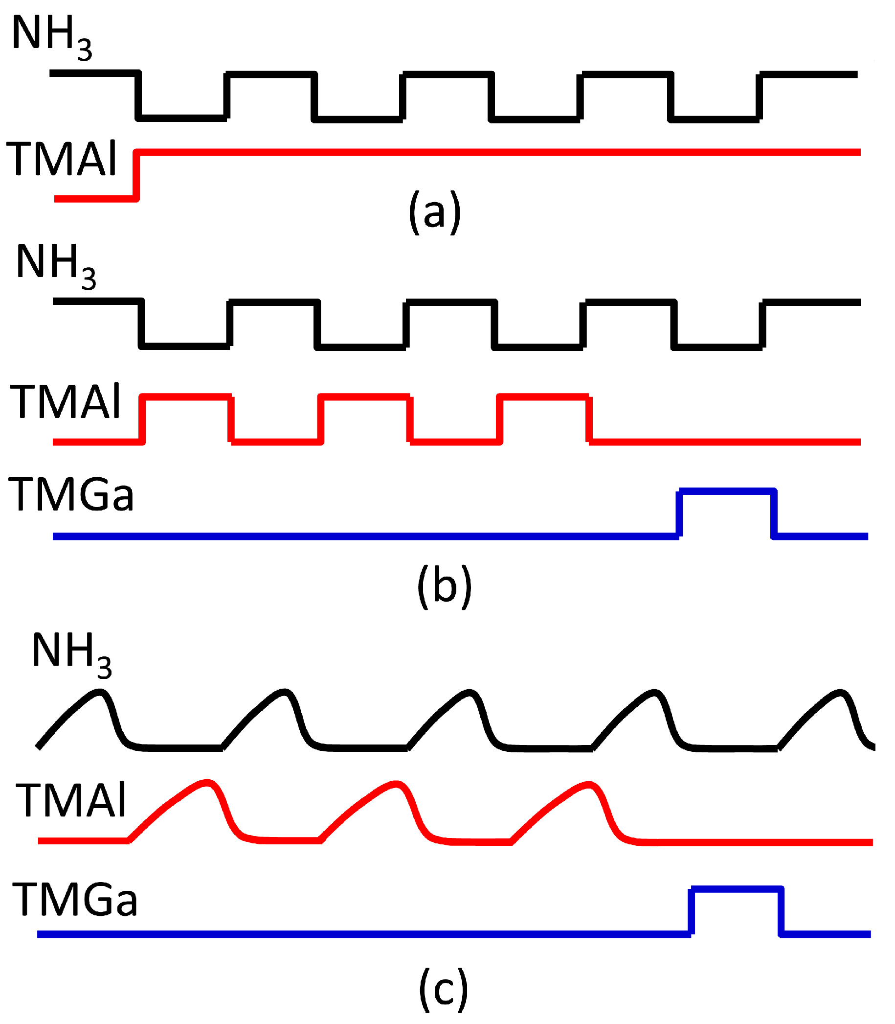
6. Pulsed-Flow Growth of AlN and High Al-Molar Fraction AlGaN

To make high-temperature growth feasible, specific modifications of MOCVD reactor hardware, including TaC-coated susceptor, BN reactor parts, and actively cooled stainless-steel gas inlets are required [59]. In order to obtain AlN and high Al-molar fraction AlGaN with high crystalline quality and flat surface morphology by using moderate growth temperatures, pulsed-flow growth methods, which can effectively promote the surface migration of Al (and Ga and In) adatoms, have been developed instead of the conventional continuous growth. There are at least three types of pulsed-flow growth methods, namely (a) NH3 pulse-flow growth [17,63,64], (b) pulsed atomic layer epitaxy (PALE) [65,66], and (c) migration-enhanced metalorganic chemical vapor deposition (MEMOCVD) [67,68,69], as shown schematically in Figure 5.
For the NH3 pulse-flow growth of AlN, pulsed NH3 flow was employed to enhance the lateral migration of Al adatoms, while TMAl flow was kept constant during the NH3 pulsed-flow sequence to ensure Al-rich growth conditions [64]. This is thought to be necessary for suppressing polarity inversion from Al to N. In order to reduce the surface roughness, continuous flow mode with high growth rate was introduced between the NH3 pulse-flow mode growth segments. By employing periodic pulsed- and continuous-flow modes, low TDD AlN layers with atomically flat surface were achieved on sapphire and Si substrates. The edge and screw-type dislocation densities in AlGaN buffer layers on AlN grown by the NH3 pulsed-flow multilayer growth technique were reported to be 7.5 × 10⁸ and 3.8 × 107 cm−2, respectively [70].
Different from the NH3 pulse-flow growth, both group III and group V precursors are sequentially modulated in the PALE method, wherein the NH3 pulse always follows the metalorganic pulses. Reduced parasitic pre-reactions and enhanced surface migration of Al adatoms, afforded by the PALE technique, promote lateral growth of AlN. FWHM values of the (0002) and (11 2 ¯ 4) reflections of XRD ω-rocking curve were reported to be less than 60 arcsec and 250 arcsec, respectively, in AlN epilayers grown at a temperature of 1070 °C [71]. The PALE approach has also been adopted for growth of high Al-molar fraction AlGaN ternary and AlInGaN quaternary layers and MQWs with very short emission wavelength (below 230 nm). This method allows accurate control of the quaternary layer composition and thickness by simply changing the number of aluminum, indium, and gallium pulses in a unit cell and the number of unit cell repeats [65,66].
MEMOCVD is carried out at relatively high temperatures (>1200 °C) and low reactor pressure conditions (<100 Torr). In contrast to PALE, the duration and waveforms of precursor pulses in MEMOCVD can be partially overlapped, allowing for a continuum of growth technique ranging from atomic layer epitaxy to conventional MOCVD. By employing MEMOCVD, a high growth rate for buffer layers and slower growth rate for active layers with reduced growth temperature and substantially improved quality can be achieved [72]. Crack-free 5- to 10-μm-thick high-quality AlN on sapphire with TDD of 2 × 108 cm−2 for all dislocation types has been grown by HT-MEMOCVD. Moreover, HT-MEMOCVD growth yielded atomically a flat surface with RMS roughness of 0.8 Å as measured by atomic force microscopy (AFM), similar to that achieved for homoepitaxial AlN on native AlN bulk substrates [69]. Combined with improved device design, MEMOCVD growth produced 278 nm AlGaN-based DUV LEDs on sapphire substrates with a maximum EQE of 10.4% at 20 mA CW current and output powers up to 9.3 mW [4].

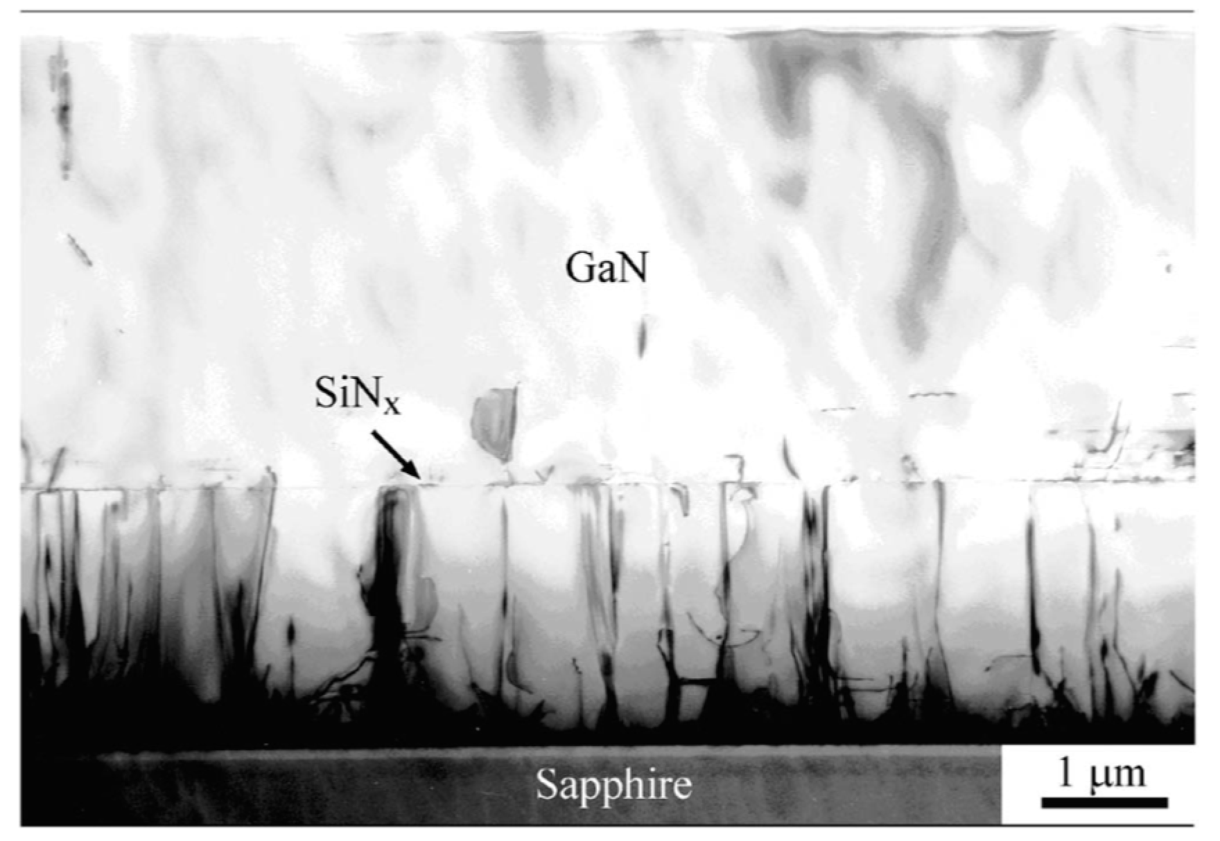
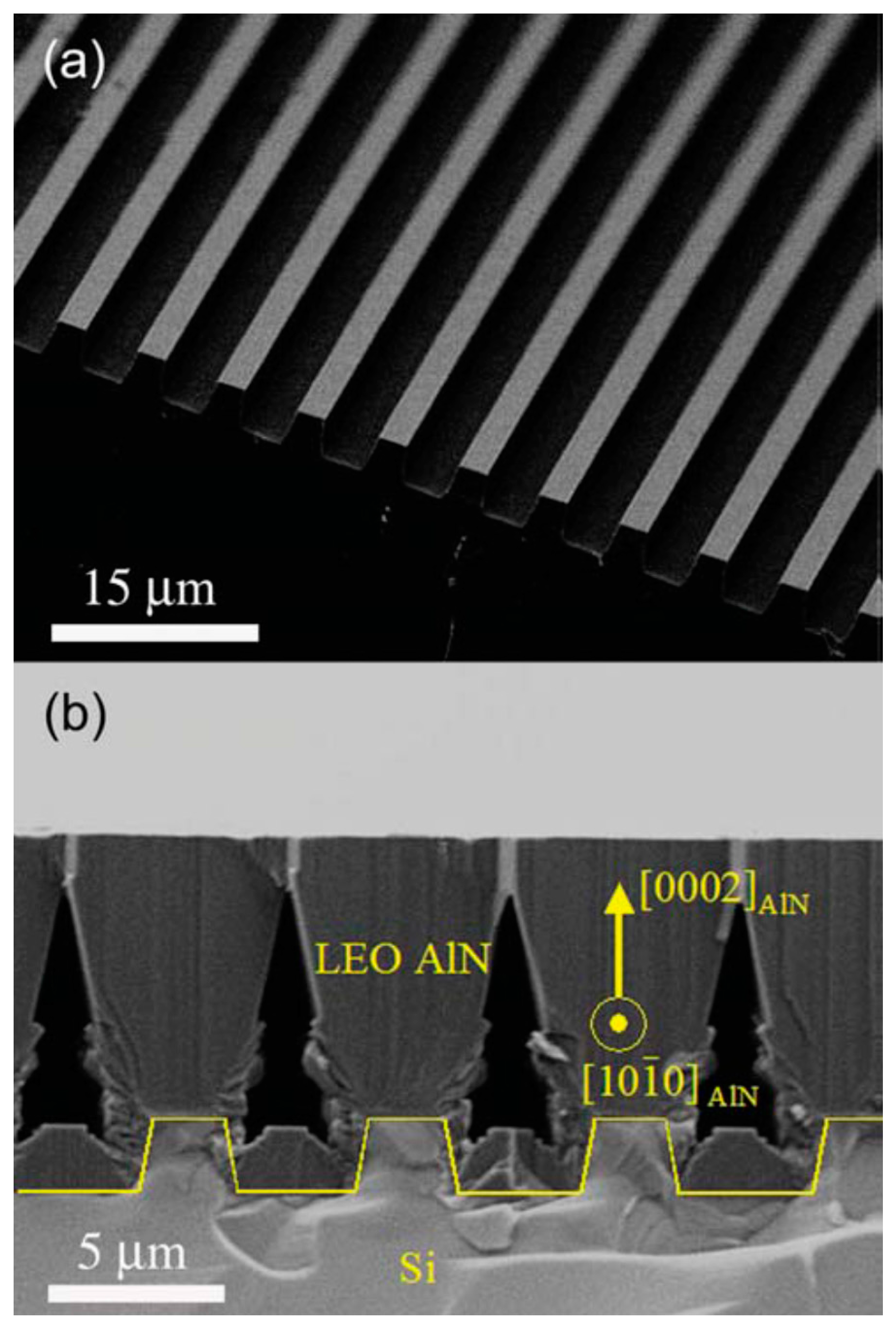
7. Epitaxial Lateral Overgrowth of AlN and High Al-Molar Fraction AlGaN

The epitaxial lateral overgrowth (ELO) technique has proven to be a useful approach for growing epilayers with low TDD on foreign substrates. It provides an avenue for DUV-LEDs with improved performance. The method relies on the growth of nitrides on windows opened in a dielectric mask material such as SiO2 or patterned substrate/template formed by etching followed by lateral extension and coalescence [73,74]. The defects can propagate to the upper layer only through the areas where there are windows, while the defect density is considerably reduced in the laterally grown area. Growth anisotropy in the form of different growth rates on different crystallographic planes plays a key role in this method [75]. One must also be concerned with defects caused by joining of advancing wings over the masked areas [76].
Due to its selectivity, the regrowth of GaN and low Al-molar fraction AlGaN commences only on the mask-free window area with no nucleation on the masked areas by the dielectric. Therefore, dielectric mask material produced by ex situ deposition and etching procedures [77] or in situ spontaneous etching [78] can be used for ELO GaN and low Al-molar fraction AlGaN. Figure 6 shows a cross-sectional transmission electron microscopy (TEM) image of an ELO GaN sample on sapphire substrate with in-situ nanoporous SiNx mask [79]. Most threading dislocations are blocked by the SiNx network, and those emanating from the pores are mostly bent into horizontal configurations.
The ELO technique with dielectric masks has also been used for TDD reduction in AlGaN with low Al-molar fraction intended for applications in LEDs in the UVA range [80]. For AlN and high Al-molar fraction AlGaN, the slow lateral growth rate of Al containing compounds and the low-selectivity between a mask and unmasked area due to large sticking coefficient of Al adatoms precludes the possibility of using dielectric masks for ELO. Maskless ELO by laterally overgrowing a trench instead of a mask material is an alternative avenue to reduce densities of both threading dislocations and cracks. ELO of AlN and high Al-molar fraction AlGaN such as Al0.96Ga0.04N on sapphire or SiC substrate have been reported by several groups [76,81,82,83]. Significant reduction in TDD was observed in the areas between ridges. A maximum output power of 2.7 mW under CW operation of 273 nm DUV LEDs on ELO AlN templates with the wing region having TDD of 3 × 108 cm−2 was reported by Hirayama et al. [84] By reducing the TDD in AlN layers on sapphire from 1010 cm−2 to 109 cm−2, output powers of 1 mW and about 4 mW for 295 nm and 324 nm LEDs, respectively, were demonstrated by Kueller et al. [73] This method has also been applied for growing AlN template on Si (111) substrate, as illustrated in Figure 7. ELO AlN templates on Si (111) substrate with FWHM values of 920 and 780 arcsec for XRD ω-rocking curves from the (0002) and (10 1 ¯ 1) reflections, respectively, with simultaneous reduction in crack density were achieved by Zhang et al. [85] A peak pulsed power and slope efficiency of ~0.6 mW and ~1.3 mW/mA, respectively, were demonstrated for 359 nm UV LEDs after removing the Si (111) substrate. In another report, FWHMs of 780 and 980 arcsec for XRD ω-rocking curves from the (0002) and (10 1 ¯ 2) reflections, respectively, were achieved in ELO AlN on Si (111). DUV LEDs with an emission wavelength of 256–278 nm exhibiting an output power of ~10 μW at a DC injection current of 140 mA without removing the Si substrate [86].

8. Pseudomorphic Growth of High Al-Molar Fraction AlGaN on AlN

Bulk AlN single crystal substrates or AlN templates with low TDD by using the abovementioned approaches offer the opportunity to grow high quality DUV LED heterostructures. However, growing lattice-matched AlGaN layer exceeding the critical thickness on AlN, results in the generation of new dislocations due to the lattice mismatch. To avoid this, pseudomorphic growth of high Al-molar fraction, AlGaN with compressive strain on AlN has been developed [58,87,88]. Because almost no new defects are generated in the pseudomorphic region, the crystalline quality of the AlGaN-based heterostructures becomes comparable to the starting substrate.
If one assumes that the Matthews and Blakeslee model is applicable, the critical thickness for AlGaN layer with an Al molar fraction of 0.6 on AlN is estimated to be only about 40 nm, which is impractically small for use in DUV LEDs. Fortunately, researchers found that, by using a transitional layer, which consisted of a linearly graded alloy with composition changed from AlN to the desired Al-molar fraction, it is possible to grow pseudomorphic AlGaN with a thickness ranging from several hundreds of nanometers to more than a micrometer, depending on the Al-molar fraction [87]. Generally, sufficiently thick pseudomorphic AlGaN layers with Al content above 70% can be grown on AlN for use in DUV LEDs with wavelengths below 280 nm, while layers with lower Al content tend to relax due to lattice mismatch. Fully pseudomorphic 500 nm thick AlGaN layers with Al content of 60% and 1 μm thick nearly pseudomorphic layers with Al content of 70% have been demonstrated [87]. The advantage of pseudomorphic growth was confirmed by XRD rocking curve measurements. For a 600 nm thick pseudomorphic Al0.72Ga0.28N layer, the FWHM values of the (0002) and (10 1 ¯ 2) reflections were 81 and 104 arcsec, respectively, compared to 64 and 89 arcsec in AlN [87]. By contrast, FWHM values of the (0002) and (10 1 ¯ 2) reflections increased from 49 and 30 arcsec, respectively, in AlN to 239 and 302 arcsec in a 500 nm thick relaxed Al0.50Ga0.50N sample.
Pseudomorphic growth has been also found to effectively improve the light extraction efficiency by switching the polarization of the emitting light. It is known that the opposite sign of the crystal field splitting energy in GaN (12.3 meV) vs. AlN (−221 meV) [34] results in the switching of the light polarization from TE in GaN to TM in AlN. The latter holds for high Al-molar fractions used to generate shorter emission wavelengths. The extraction efficiency of TM-polarized light is one order of magnitude lower than that of TE-polarized light, which is one of the critical factors that limit the EQE of AlGaN-based DUV LEDs. Several studies showed that the light generated using AlGaN-based heterostructures switches its polarization from TE to TM mode for Al-molar fractions anywhere between 20% and 40% [89,90]. Recently, Sharma et al. demonstrated theoretically that the critical Al-molar fraction at which the polarization switches depends on the amount of residual strain in the AlGaN layer [91]. In pseudomorphically grown AlGaN, the critical Al-molar fraction for polarization switching can be as high as 80%. Figure 8 shows the degree of polarization of emission from LEDs fabricated on sapphire or AlN substrates [92]. The tendency for the polarization of the emitted light to switch from TE polarization to TM polarization with decreasing wavelength is clearly seen in the figure. However, Device 1 pseudomorphically grown on AlN substrate emits highly TE-polarized light with a wavelength of 253 nm. According to theoretical computations [92], the switch of polarization from TE to TM depends on the strain in the quantum well. For an active region that is pseudomorphic to bulk AlN, aQW-abulk-AlN = 0, and the expected polarization is TE, which is the case of Device 1. For Devices 2–4 grown on sapphire, it was proposed that the strain state of the active regions corresponds to aQW-abulk-AlN >0.01 Å. The compressive strain in the active region of these devices is less than that required for TE polarization; therefore, showing strong TM-polarized emission. Reich et al. [93] demonstrated that, by using narrow QWs and high Al content barrier on compressively strained ELO AlN/sapphire templates, strongly TE-polarized emission was achieved for pseudomorphic DUV LEDs with emission wavelength as short as 239 nm.
Improvement of device performance through pseudomorphic growth has also been demonstrated by several groups [3,10,88]. A high IQE value of ~80% at a photo-generated carrier density of 1018 cm−3 was achieved in UVC MQW structures emitting at ~258 nm, which were pseudomorphically grown on bulk AlN substrates that contain less than 103 cm−2 dislocations [46], as revealed by synchrotron white-beam X-ray topography [94]. In an encapsulated pseudomorphic LED structure with improved LEE, through thinned AlN substrate, an output power of over 60 mW and an EQE of 4.9% were realized in continuous wave operation [3]. Pseudomorphic LEDs also show improved lifetimes and reliability. LEDs of 266 nm tested, in both surface mount design and TO-39 package, showed lifetimes above 1000 h under a variety of case temperatures and currents using performance degradation of 50% as the marker [10].

9. AlN/AlGaN Superlattice Buffer

One important approach used to improve the material quality of AlGaN-based heterosturctures is via AlN/AlGaN (or AlGaN/AlGaN) superlattice buffer. The utility of AlN/AlGaN superlattice in relieving strain for DUV LEDs was proposed as far back as in 2002. Zhang et al. [95] demonstrated the utility of ten period AlN/Al0.2Ga0.8N superlattices, inserted between HT-AlN/LT-AlN/sapphire composite and the n-type AlGaN layer, in significantly reducing the biaxial tensile strain in the n-AlGaN layer, allowing 3 μm thick crack-free Al0.2Ga0.8N films. Later Wang et al. [96] reported that AlN/AlGaN superlattice buffer also acts as a dislocation filter for TDD reduction in AlGaN layers on sapphire substrate. This buffer was found to greatly enlarge the coherence lengths of mosaic blocks and reduce the TDD by two orders of magnitude in Al0.2Ga0.8N layers. Xi et al. [97] conducted a comparative study of n-type AlGaN grown on sapphire by using a superlattice buffer and a LT-AlN interlayer. Improved electrical properties with higher electron concentration and mobility and surface morphologies, lacking hexagonal hillocks on the Al0.3Ga0.7N surface, was achieved in samples with AlN/AlGaN or AlGaN/AlGaN superlattice buffer, compared with samples with only a LT-AlN interlayer buffer [97].
Chitnis et al. [98] also demonstrated improved performance in DUV LEDs with AlN/AlGaN superlattice buffer layer. By using the pulsed atomic layer epitaxy (PALE) approach discussed in Section 6, and an AlN/Al0.85Ga0.15N superlattice strain-relief buffer, output power levels of 10.2 mW at 1 A pulsed current and 1 mW at 100 mA CW current were achieved in LEDs emitting at 325 nm and grown on sapphire substrates. In recently developed high-power DUV LEDs, the AlN/AlGaN superlattice buffer approach was employed by several groups [4,16]. For example, the LEDs emitting at 278 nm with an EQE of 10.4% and an output power of 9.3 mW at 20 mA CW current utilized strain-relief AlN/AlGaN superlattices on 10 μm thick AlN layers by migration-enhanced metalorganic chemical vapor deposition (MEMOCVD) [4]. In 255, 280, and 310 nm DUV LEDs with output powers of 45.2, 93.3, and 65.8 mW and EQEs of 1.3%, 3.0%, and 2.4%, respectively, at 350 mA pulsed current, AlN/AlGaN superlattices were also implemented as a basic design strategy for strain-relief [16].

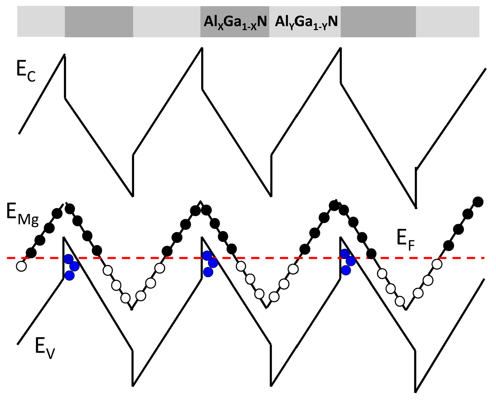
10. Doping Considerations in High Al-Molar Fraction AlGaN

As is well known, the remarkable progress in group III-nitride LEDs hinged on the achievement of p-type doping in GaN. However, non-transparency of p-GaN for emission wavelengths below 365 nm leads to significant self-absorption and a very low LEE of DUV LEDs. In addition, the large barrier between p-type GaN and high Al-molar fraction AlGaN electron blocking layer (EBL) hinders the injection efficiency of holes. To overcome these obstacles, researchers have focused on developing transparent p-AlGaN with improved hole conductivity to replace the p-GaN layer [8], as schematically shown in Figure 9. The factors limiting the conductivity of p-AlGaN include severe self-compensation by donor-like defects that are produced simultaneously, limited dopant solubility, and increasingly high acceptor activation energy of Mg dopant with increasing Al molar fraction—the activation energy reaches ~400 meV for an Al fraction of 70% [99], and is as high as 510~630 meV for AlN [100,101]. Therefore, numerous efforts have been undertaken to mitigate compensation by decreasing donor defects and increasing solubility of the dopants, increasing the hole mobility by reducing the scattering rate, and increasing the acceptor activation rate by reducing the activation energy through polarization field. The approaches include co-doping of Mg with Si or oxygen [102,103], Mg delta-doping [104,105], and Mg-doped AlxGa1-xN/AlN superlattice or AlxGa1-xN/AlyGa1-yN superlattice [106,107]. Some of the reports on the achievement of low p-type resistivities in high Al-molar fraction AlGaN are overviewed below.
Kakanakova-Georgieva et al. estimated a hole concentration of ~1014 cm−3 for Mg-doped Al0.85Ga0.15N layers, from the a room temperature resistivity of 7 kΩ cm by assuming a hole mobility of 2 cm2V−1s−1, when grown using a hot wall MOCVD system which purportedly leads to growth conditions for reduced compensation by native defects [108]. The same authors also reported a resistivity of 2 kΩ cm and 60 Ω cm for Al0.70Ga0.30N and Al0.60Ga0.40N, respectively, by using the hot wall MOCVD reactor with optimized V/III ratio [109]. If the same hole mobility of 2 cm2V−1s−1 is assumed, the hole concentrations in the Al0.70Ga0.30N and Al0.60Ga0.40N layers are deduced to be ~3.5 × 1014 cm−3 and ~1 × 1016 cm−3, respectively. Through the optimization of growth conditions, highly conductive p-type Mg-doped Al0.70Ga0.30N thin films were realized by employing a high V/III ratio and moderate Mg concentration by Kinoshita et al. [110] Such conditions were found to effectively suppress self-compensation by the formation of nitrogen vacancy complexes, which are considered to be the compensating donors. An electrical resistivity as low as 47 Ω cm and a hole concentration of 1.3 × 1017 cm−3 was achieved with an Mg concentration of 3.9 × 1019 cm−3 at room temperature.
Mg-doped AlxGa1-xN/AlN superlattice or AlxGa1-xN/AlyGa1-yN superlattice with alternating low and high Al composition has been employed to obtain relatively high p-type conductivity [106,107]. The mechanism for hole enhancement is the periodic modulation of the valence-band edge. Acceptors are ionized where the band edge is far below the Fermi energy set by the lower Al-molar fraction regions, and the resulting holes accumulate where the band edge is close to the Fermi level, forming a confined sheet of carriers, as schematically illustrated in Figure 10. Although the free carriers are separated into parallel sheets, their spatially averaged density will be much higher than in a standard bulk film. The effective activation energy was determined to be 29 meV in Mg-doped AlxGa1-xN/AlN superlattices with an average Al composition of 0.62, and 18 meV with an average Al composition of 0.49 [106]. P-type resistivities below 10 Ω cm were measured in superlattice structures with an average Al composition from 0.49 to 0.74. As an additional benefit, AlxGa1-xN/AlN superlattices with periods of 20 Å or less have shown optical transparency similar to random alloy AlxGa1-xN epilayers of the same average composition, indicating the potential of this approach for DUV LEDs [106].
Compared with p-type doping, n-type doping of high Al-molar fraction AlGaN is relatively straightforward. For AlGaN with Al-molar fraction below 50%, the activation energy of Si remains at very low values similar to that in GaN (15–25 meV) [44]. Therefore the Si dopants can still be almost completely activated, and electron concentrations above 1018 cm−3 are typically obtained. For AlGaN with Al-molar fraction above 80%, both the activation energy of Si dopants and the self-compensation effect increase sharply with increasing Al-molar fraction [100,111]. These result in a rapid drop in the achievable electron concentrations with increasing Al-molar fraction. Taking advantage of the pseudomorphic growth, electrical resistivities below 0.1 Ω cm were reported by Collazo et al. [44] for n-type AlGaN films with Al-molar fraction below 85% grown pseudomorphically on bulk AlN. An electron concentration of ~1 × 1018 cm−3 and an electron mobility above 40 cm2/Vs were obtained for a film with Al-molar fraction of 80% and a Si doping concentration of 6 × 1018 cm−3 [44]. By optimizing SiH4/group-III ratio, Mehnke et al. [112] achieved a resistivity of 0.026 Ω cm for Al0.81Ga0.19N epilayers pseudomorphically grown on low defect density ELO AlN/sapphire templates, with an electron concentration of 1.5 × 1019 cm−3 and a mobility of 16.5 cm2/Vs. These values are thought to be sufficient for efficient operation of DUV LEDs with an emission wavelength of 250–260 nm.

11. Conclusions

We have provided a succinct overview of the recent progress in growth of III-nitride heterostructures for DUV LEDs, with particular emphasis on growth of AlN and growth and doping of high Al-molar fraction AlGaN. Although at this stage, the efficiency of DUV LEDs is behind those operating in the near UV and the visible spectra ranges, one can be optimistic in that the efficiencies and output powers of DUV LEDs will continue to increase in the near future and EQEs of tens of percent are achievable. Homoepitaxial growth on bulk AlN crystals looks attractive barring cost concerns. The developments in bulk AlN single crystals have already led to superior device performance as compared to those on foreign substrates owing to reduced defect density in the films. Wider applications on AlN bulk crystal substrates are expected with further improvements in the bulk crystal growth technologies together with needed reduction in cost. Pseudomorphic growth of strained AlGaN has shown the capability of growing high-quality epilayers with TDDs comparable to the starting substrate and driving the critical Al-molar fraction up to 80%, at which polarization of emitted light switches from TE to TM mode, thus improving both IQE and light extraction efficiency. Optimized heterostructure design, which includes AlGaN multi-quantum barrier as electron blocking layer, has enabled a marked increase in electron injection efficiency. New strategies such as AlN pillar arrays, sidewall emission-enhanced chip geometry, and durable encapsulation have also shown their potential in light extraction enhancement. The combination of advanced material growth approaches, device design, and light extraction strategies stand to make DUV LEDs more efficient in the future.

Acknowledgments

The authors would like to thank M. Kneissl of Technische Universität Berlin for providing the original version of Figure 1.

Author Contributions

All the authors have participated in the literature review and in the correction and revision of the manuscript.

Conflicts of Interest

The authors declare no conflict of interest.

References

  1. Pernot, C.; Kim, M.; Fukahori, S.; Inazu, T.; Fujita, T.; Nagasawa, Y.; Hirano, A.; Ippommatsu, M.; Iwaya, M.; Kamiyama, S.; et al. Improved efficiency of 255–280 nm AlGaN-based light-emitting diodes. Appl. Phys. Express 2010, 3, 061004. [Google Scholar] [CrossRef]
  2. Grandusky, J.R.; Gibb, S.R.; Mendrick, M.C.; Moe, C.; Wraback, M.; Schowalter, L.J. High output power from 260 nm pseudomorphic ultraviolet light-emitting diodes with improved thermal performance. Appl. Phys. Express 2011, 4, 082101. [Google Scholar] [CrossRef]
  3. Grandusky, J.R.; Chen, J.; Gibb, S.R.; Mendrick, M.C.; Moe, C.G.; Rodak, L.; Garrett, G.A.; Wraback, M.; Schowalter, L.J. 270 nm pseudomorphic ultraviolet light-emitting diodes with over 60 mw continuous wave output power. Appl. Phys. Express 2013, 6, 032101. [Google Scholar] [CrossRef]
  4. Shatalov, M.; Sun, W.; Lunev, A.; Hu, X.; Dobrinsky, A.; Bilenko, Y.; Yang, J.; Shur, M.; Gaska, R.; Moe, C.; et al. AlGaN deep-ultraviolet light-emitting diodes with external quantum efficiency above 10%. Appl. Phys. Express 2012, 5, 082101. [Google Scholar] [CrossRef]
  5. Inoue, S.-I.; Naoki, T.; Kinoshita, T.; Obata, T.; Yanagi, H. Light extraction enhancement of 265 nm deep-ultraviolet light-emitting diodes with over 90 mw output power via an AlN hybrid nanostructure. Appl. Phys. Lett. 2015, 106, 131104. [Google Scholar] [CrossRef]
  6. Maeda, N.; Hirayama, H. Realization of high-efficiency deep-UV LEDs using transparent p-AlGaN contact layer. Phys. Stat. Sol. C 2013, 10, 1521–1524. [Google Scholar] [CrossRef]
  7. Hirayama, H.; Takano, T.; Sakai, J.; Mino, T.; Tsubaki, K.; Maeda, N.; Jo, M.; Kanazawa, Y.; Ohshima, I.; Matsumoto, T. Realization of Over 10% EQE AlGaN Deep-UV LED by Using Transparent p-AlGaN Contact Layer. In Proceedings of the 2016 International Semiconductor Laser Conference (ISLC), 12–15 September 2016; pp. 1–2. [Google Scholar]
  8. Takano, T.; Mino, T.; Sakai, J.; Noguchi, N.; Tsubaki, K.; Hirayama, H. Deep-ultraviolet light-emitting diodes with external quantum efficiency higher than 20% at 275 nm achieved by improving light-extraction efficiency. Appl. Phys. Express 2017, 10, 031002. [Google Scholar] [CrossRef]
  9. Kinoshita, T.; Obata, T.; Nagashima, T.; Yanagi, H.; Moody, B.; Mita, S.; Inoue, S.-I.; Kumagai, Y.; Koukitu, A.; Sitar, Z. Performance and reliability of deep-ultraviolet light-emitting diodes fabricated on AlN substrates prepared by hydride vapor phase epitaxy. Appl. Phys. Express 2013, 6, 092103. [Google Scholar] [CrossRef]
  10. Moe, C.G.; Grandusky, J.R.; Chen, J.; Kitamura, K.; Mendrick, M.C.; Jamil, M.; Toita, M.; Gibb, S.R.; Schowalter, L.J. High-power pseudomorphic mid-ultraviolet light-emitting diodes with improved efficiency and lifetime. Proc. SPIE 2014, 8986, 89861V. [Google Scholar]
  11. Hwang, S.; Morgan, D.; Kesler, A.; Lachab, M.; Zhang, B.; Heidari, A.; Nazir, H.; Ahmad, I.; Dion, J.; Fareed, Q.; et al. 276 nm substrate-free flip-chip AlGaN light-emitting diodes. Appl. Phys. Express 2011, 4, 032102. [Google Scholar] [CrossRef]
  12. Fujioka, A.; Misaki, T.; Murayama, T.; Narukawa, Y.; Mukai, T. Improvement in output power of 280-nm deep ultraviolet light-emitting diode by using AlGaN multi quantum wells. Appl. Phys. Express 2010, 3, 041001. [Google Scholar] [CrossRef]
  13. Kneissl, M.; Kolbe, T.; Chua, C.; Kueller, V.; Lobo, N.; Stellmach, J.; Knauer, A.; Rodriguez, H.; Einfeldt, S.; Yang, Z.; et al. Advances in group III-nitride-based deep UV light-emitting diode technology. Semicon. Sci. Tech. 2011, 26, 014036. [Google Scholar] [CrossRef]
  14. Kolbe, T.; Mehnke, F.; Guttmann, M.; Kuhn, C.; Rass, J.; Wernicke, T.; Kneissl, M. Improved injection efficiency in 290 nm light emitting diodes with Al(Ga)N electron blocking heterostructure. Appl. Phys. Lett. 2013, 103, 031109. [Google Scholar] [CrossRef]
  15. Dong, P.; Yan, J.; Wang, J.; Zhang, Y.; Geng, C.; Wei, T.; Cong, P.; Zhang, Y.; Zeng, J.; Tian, Y.; et al. 282-nm AlGaN-based deep ultraviolet light-emitting diodes with improved performance on nano-patterned sapphire substrates. Appl. Phys. Lett. 2013, 102, 241113. [Google Scholar] [CrossRef]
  16. Fujioka, A.; Asada, K.; Yamada, H.; Ohtsuka, T.; Ogawa, T.; Kosugi, T.; Kishikawa, D.; Mukai, T. High-output-power 255/280/310 nm deep ultraviolet light-emitting diodes and their lifetime characteristics. Semicon. Sci. Tech. 2014, 29, 084005. [Google Scholar] [CrossRef]
  17. Hirayama, H.; Maeda, N.; Fujikawa, S.; Toyoda, S.; Kamata, N. Recent progress and future prospects of AlGaN-based high-efficiency deep-ultraviolet light-emitting diodes. Jpn. J. Appl. Phys. 2014, 53, 100209. [Google Scholar] [CrossRef]
  18. Kneissl, M.; Rass, J. III-Nitride Ultraviolet Emitters. In Springer Series in Materials Science; Springer International Publishing: Cham, Switzerland, 2016; Volume 277. [Google Scholar]
  19. Hirayama, H. Growth techniques of AlN/AlGaN and development of high-efficiency deep-ultraviolet light-emitting diodes. In III-Nitride Ultraviolet Emitters; Springer: Berlin, Germany, 2016; pp. 75–113. [Google Scholar]
  20. Hirayama, H.; Fujikawa, S.; Kamata, N. Recent progress in ALGaN-based deep-UV LEDs. Electron. Commun. Jpn. 2015, 98, 1–8. [Google Scholar] [CrossRef]
  21. Yasan, A.; McClintock, R.; Mayes, K.; Shiell, D.; Gautero, L.; Darvish, S.R.; Kung, P.; Razeghi, M. 4.5 mw operation of AlGaN-based 267 nm deep-ultraviolet light-emitting diodes. Appl. Phys. Lett. 2003, 83, 4701–4703. [Google Scholar] [CrossRef]
  22. Shatalov, M.; Chitnis, A.; Yadav, P.; Hasan, M.F.; Khan, J.; Adivarahan, V.; Maruska, H.P.; Sun, W.H.; Khan, M.A. Thermal analysis of flip-chip packaged 280 nm nitride-based deep ultraviolet light-emitting diodes. Appl. Phys. Lett. 2005, 86, 201109. [Google Scholar] [CrossRef]
  23. Ryu, H.-Y.; Choi, I.-G.; Choi, H.-S.; Shim, J.-I. Investigation of light extraction efficiency in AlGaN deep-ultraviolet light-emitting diodes. Appl. Phys. Express 2013, 6, 062101. [Google Scholar] [CrossRef]
  24. Inoue, S.-I.; Tamari, N.; Taniguchi, M. 150 mw deep-ultraviolet light-emitting diodes with large-area AlN nanophotonic light-extraction structure emitting at 265 nm. Appl. Phys. Lett. 2017, 110, 141106. [Google Scholar] [CrossRef]
  25. Kim, D.Y.; Park, J.H.; Lee, J.W.; Hwang, S.; Oh, S.J.; Kim, J.; Sone, C.; Schubert, E.F.; Kim, J.K. Overcoming the fundamental light-extraction efficiency limitations of deep ultraviolet light-emitting diodes by utilizing transverse-magnetic-dominant emission. Light Sci. Appl. 2015, 4, e263. [Google Scholar] [CrossRef]
  26. Lee, J.W.; Kim, D.Y.; Park, J.H.; Schubert, E.F.; Kim, J.; Lee, J.; Kim, Y.I.; Park, Y.; Kim, J.K. An elegant route to overcome fundamentally-limited light extraction in AlGaN deep-ultraviolet light-emitting diodes: Preferential outcoupling of strong in-plane emission. Sci. Rep. 2016, 6, 22537. [Google Scholar] [CrossRef] [PubMed]
  27. Ichikawa, M.E.S.; Sagawa, H.; Fujioka, A.; Kosugi, T.; Mukai, T.; Uomoto, M.; Shimatsu, T. High output power deep ultraviolet light-emitting diodes with hemispherical lenses fabricated using room temperature bonding. ECS Trans. 2016, 75, 53–65. [Google Scholar] [CrossRef]
  28. Nagai, S.; Yamada, K.; Hirano, A.; Ippommatsu, M.; Ito, M.; Morishima, N.; Aosaki, K.; Honda, Y.; Amano, H.; Akasaki, I. Development of highly durable deep-ultraviolet AlGaN-based led multichip array with hemispherical encapsulated structures using a selected resin through a detailed feasibility study. Jpn. J. Appl. Phys. 2016, 55, 082101. [Google Scholar] [CrossRef]
  29. Yamada, K.; Furusawa, Y.; Nagai, S.; Hirano, A.; Ippommatsu, M.; Aosaki, K.; Morishima, N.; Amano, H.; Akasaki, I. Development of underfilling and encapsulation for deep-ultraviolet LEDs. Appl. Phys. Express 2015, 8, 012101. [Google Scholar] [CrossRef]
  30. Hirano, A.; Nagasawa, Y.; Ippommatsu, M.; Aosaki, K.; Honda, Y.; Amano, H.; Akasaki, I. Development of AlGaN-based deep-ultraviolet (DUV) LEDs focusing on the fluorine resin encapsulation and the prospect of the practical applications. Proc. SPIE 2016, 9926, 99260C. [Google Scholar]
  31. Fujito, K.; Kubo, S.; Nagaoka, H.; Mochizuki, T.; Namita, H.; Nagao, S. Bulk GaN crystals grown by HVPE. J. Cryst. Growth 2009, 311, 3011–3014. [Google Scholar] [CrossRef]
  32. Dwiliński, R.; Doradziński, R.; Garczyński, J.; Sierzputowski, L.; Kucharski, R.; Zając, M.; Rudziński, M.; Kudrawiec, R.; Strupiński, W.; Misiewicz, J. Ammonothermal GaN substrates: Growth accomplishments and applications. Phys. Stat. Sol. A 2011, 208, 1489–1493. [Google Scholar] [CrossRef]
  33. Levinshtein, M.E.; Rumyantsev, S.L.; Shur, M.S. Properties of Advanced Semiconductor Materials: GaN, AlN, InN, BN, SiC, SiGe; John Wiley & Sons: Hoboken, NJ, USA, 2001. [Google Scholar]
  34. Morkoç, H. Handbook of Nitride Semiconductors and Devices, Materials Properties, Physics and Growth; John Wiley & Sons: Hoboken, NJ, USA, 2009; Volume 1. [Google Scholar]
  35. Mueller, S.G.; Bondokov, R.T.; Morgan, K.E.; Slack, G.A.; Schujman, S.B.; Grandusky, J.; Smart, J.A.; Schowalter, L.J. The progress of AlN bulk growth and epitaxy for electronic applications. Phys. Stat. Sol. A 2009, 206, 1153–1159. [Google Scholar] [CrossRef]
  36. Ehrentraut, D.; Sitar, Z. Advances in bulk crystal growth of AlN and GaN. MRS Bull. 2009, 34, 259–265. [Google Scholar] [CrossRef]
  37. Herro, Z.G.; Zhuang, D.; Schlesser, R.; Collazo, R.; Sitar, Z. Seeded growth of AlN on N- and Al-polar AlN seeds by physical vapor transport. J. Cryst. Growth 2006, 286, 205–208. [Google Scholar] [CrossRef]
  38. Helava, H.; Chemekova, T.J.; Avdeev, O.; Mokhov, E.; Nagalyuk, S.; Makarov, Y.; Ramm, M. AlN substrates and epitaxy results. Phys. Stat. Sol. C 2010, 7, 2115–2117. [Google Scholar] [CrossRef]
  39. Herro, Z.G.; Zhuang, D.; Schlesser, R.; Sitar, Z. Growth of AlN single crystalline boules. J. Cryst. Growth 2010, 312, 2519–2521. [Google Scholar] [CrossRef]
  40. Nagai, I.; Kato, T.; Miura, T.; Kamata, H.; Naoe, K.; Sanada, K.; Okumura, H. AlN bulk single crystal growth on 6H-SiC substrates by sublimation method. J. Cryst. Growth 2010, 312, 2699–2704. [Google Scholar] [CrossRef]
  41. Makarov, Y.N.; Avdeev, O.V.; Barash, I.S.; Bazarevskiy, D.S.; Chemekova, T.Y.; Mokhov, E.N.; Nagalyuk, S.S.; Roenkov, A.D.; Segal, A.S.; Vodakov, Y.A.; et al. Experimental and theoretical analysis of sublimation growth of AlN bulk crystals. J. Cryst. Growth 2008, 310, 881–886. [Google Scholar] [CrossRef]
  42. Hartmann, C.; Dittmar, A.; Wollweber, J.; Bickermann, M. Bulk AlN growth by physical vapour transport. Semicon. Sci. Tech. 2014, 29, 084002. [Google Scholar] [CrossRef]
  43. Ren, Z.; Sun, Q.; Kwon, S.Y.; Han, J.; Davitt, K.; Song, Y.K.; Nurmikko, A.V.; Liu, W.; Smart, J.; Schowalter, L. AlGaN deep ultraviolet LEDs on bulk AlN substrates. Phys. Stat. Sol. C 2007, 4, 2482–2485. [Google Scholar] [CrossRef]
  44. Collazo, R.; Mita, S.; Xie, J.; Rice, A.; Tweedie, J.; Dalmau, R.; Sitar, Z. Progress on n-type doping of AlGaN alloys on AlN single crystal substrates for UV optoelectronic applications. Phys. Stat. Sol. C 2011, 8, 2031–2033. [Google Scholar] [CrossRef]
  45. Grandusky, J.R.; Gibb, S.R.; Mendrick, M.C.; Schowalter, L.J. Properties of mid-ultraviolet light emitting diodes fabricated from pseudomorphic layers on bulk aluminum nitride substrates. Appl. Phys. Express 2010, 3, 072103. [Google Scholar] [CrossRef]
  46. Bryan, Z.; Bryan, I.; Xie, J.; Mita, S.; Sitar, Z.; Collazo, R. High internal quantum efficiency in AlGaN multiple quantum wells grown on bulk AlN substrates. Appl. Phys. Lett. 2015, 106, 142107. [Google Scholar] [CrossRef]
  47. Bickermann, M.; Epelbaum, B.M.; Filip, O.; Heimann, P.; Nagata, S.; Winnacker, A. UV transparent single-crystalline bulk AlN substrates. Phys. Stat. Sol. C 2010, 7, 21–24. [Google Scholar] [CrossRef]
  48. Bickermann, M.; Epelbaum, B.M.; Filip, O.; Tautz, B.; Heimann, P.; Winnacker, A. Faceting in AlN bulk crystal growth and its impact on optical properties of the crystals. Phys. Stat. Sol. C 2012, 9, 449–452. [Google Scholar] [CrossRef]
  49. Tuomisto, F.; Mäki, J.M.; Chemekova, T.Y.; Makarov, Y.N.; Avdeev, O.V.; Mokhov, E.N.; Segal, A.S.; Ramm, M.G.; Davis, S.; Huminic, G.; et al. Characterization of bulk AlN crystals with positron annihilation spectroscopy. J. Cryst. Growth 2008, 310, 3998–4001. [Google Scholar] [CrossRef]
  50. Sumathi, R.R.; Gille, P. Development and progress in bulk c-plane AlN single-crystalline template growth for large-area native seeds. Jpn. J. Appl. Phys. 2013, 52, 08JA02. [Google Scholar] [CrossRef]
  51. Collazo, R.; Xie, J.; Gaddy, B.E.; Bryan, Z.; Kirste, R.; Hoffmann, M.; Dalmau, R.; Moody, B.; Kumagai, Y.; Nagashima, T.; et al. On the origin of the 265 nm absorption band in AlN bulk crystals. Appl. Phys. Lett. 2012, 100, 191914. [Google Scholar] [CrossRef]
  52. Hartmann, C.; Wollweber, J.; Dittmar, A.; Irmscher, K.; Kwasniewski, A.; Langhans, F.; Neugut, T.; Bickermann, M. Preparation of bulk AlN seeds by spontaneous nucleation of freestanding crystals. Jpn. J. Appl. Phys. 2013, 52, 08JA06. [Google Scholar] [CrossRef]
  53. Sedhain, A.; Du, L.; Edgar, J.H.; Lin, J.Y.; Jiang, H.X. The origin of 2.78 ev emission and yellow coloration in bulk AlN substrates. Appl. Phys. Lett. 2009, 95, 262104. [Google Scholar] [CrossRef]
  54. Kumagai, Y.; Enatsu, Y.; Ishizuki, M.; Kubota, Y.; Tajima, J.; Nagashima, T.; Murakami, H.; Takada, K.; Koukitu, A. Investigation of void formation beneath thin AlN layers by decomposition of sapphire substrates for self-separation of thick AlN layers grown by HVPE. J. Cryst. Growth 2010, 312, 2530–2536. [Google Scholar] [CrossRef]
  55. Kumagai, Y.; Nagashima, T.; Koukitu, A. Preparation of a freestanding AlN substrate by hydride vapor phase epitaxy at 1230 c using (111) Si as a starting substrate. Jpn. J. Appl. Phys. 2007, 46, L389. [Google Scholar] [CrossRef]
  56. Nomura, T.; Okumura, K.; Miyake, H.; Hiramatsu, K.; Eryu, O.; Yamada, Y. AlN homoepitaxial growth on sublimation-AlN substrate by low-pressure HVPE. J. Cryst. Growth 2012, 350, 69–71. [Google Scholar] [CrossRef]
  57. Kumagai, Y.; Kubota, Y.; Nagashima, T.; Kinoshita, T.; Dalmau, R.; Schlesser, R.; Moody, B.; Xie, J.; Murakami, H.; Koukitu, A.; et al. Preparation of a freestanding AlN substrate from a thick AlN layer grown by hydride vapor phase epitaxy on a bulk AlN substrate prepared by physical vapor transport. Appl. Phys. Express 2012, 5, 055504. [Google Scholar] [CrossRef]
  58. Kinoshita, T.; Hironaka, K.; Obata, T.; Nagashima, T.; Dalmau, R.; Schlesser, R.; Moody, B.; Xie, J.; Inoue, S.-i.; Kumagai, Y.; et al. Deep-ultraviolet light-emitting diodes fabricated on AlN substrates prepared by hydride vapor phase epitaxy. Appl. Phys. Express 2012, 5, 122101. [Google Scholar] [CrossRef]
  59. Brunner, F.; Protzmann, H.; Heuken, M.; Knauer, A.; Weyers, M.; Kneissl, M. High-temperature growth of AlN in a production scale 11 × 2’ movpe reactor. Phys. Stat. Sol. C 2008, 5, 1799–1801. [Google Scholar] [CrossRef]
  60. Chichibu, S.F.; Onuma, T.; Hazu, K.; Uedono, A. Major impacts of point defects and impurities on the carrier recombination dynamics in AlN. Appl. Phys. Lett. 2010, 97, 201904. [Google Scholar] [CrossRef]
  61. Chichibu, S.F.; Onuma, T.; Hazu, K.; Uedono, A. Time-resolved luminescence studies on AlN and high AlN mole fraction AlGaN alloys. Phys. Stat. Sol. C 2013, 10, 501–506. [Google Scholar] [CrossRef]
  62. Onuma, T.; Hazu, K.; Uedono, A.; Sota, T.; Chichibu, S.F. Identification of extremely radiative nature of AlN by time-resolved photoluminescence. Appl. Phys. Lett. 2010, 96, 061906. [Google Scholar] [CrossRef]
  63. Hirayama, H.; Fujikawa, S.; Noguchi, N.; Norimatsu, J.; Takano, T.; Tsubaki, K.; Kamata, N. 222–282 nm AlGaN and in AlGaN-based deep-UV LEDs fabricated on high-quality AlN on sapphire. Phys. Stat. Sol. A 2009, 206, 1176–1182. [Google Scholar] [CrossRef]
  64. Hirayama, H.; Yatabe, T.; Noguchi, N.; Ohashi, T.; Kamata, N. 231–261nm AlGaN deep-ultraviolet light-emitting diodes fabricated on AlN multilayer buffers grown by ammonia pulse-flow method on sapphire. Appl. Phys. Lett. 2007, 91, 071901. [Google Scholar] [CrossRef]
  65. Zhang, J.; Kuokstis, E.; Fareed, Q.; Wang, H.; Yang, J.; Simin, G.; Khan, M.A.; Gaska, R.; Shur, M. Pulsed atomic layer epitaxy of quaternary AlInGaN layers. Appl. Phys. Lett. 2001, 79, 925–927. [Google Scholar] [CrossRef]
  66. Zhang, J.P.; Khan, M.A.; Sun, W.H.; Wang, H.M.; Chen, C.Q.; Fareed, Q.; Kuokstis, E.; Yang, J.W. Pulsed atomic-layer epitaxy of ultrahigh-quality AlxGa1−xN structures for deep ultraviolet emissions below 230 nm. Appl. Phys. Lett. 2002, 81, 4392–4394. [Google Scholar] [CrossRef]
  67. Bilenko, Y.; Lunev, A.; Hu, X.; Deng, J.; Katona, T.M.; Zhang, J.; Gaska, R.; Shur, M.S.; Sun, W.; Adivarahan, V. 10 milliwatt pulse operation of 265 nm AlGaN light emitting diodes. Jpn. J. Appl. Phys. 2004, 44, L98. [Google Scholar] [CrossRef]
  68. Sun, W.H.; Yang, J.W.; Zhang, J.P.; Gaevski, M.E.; Chen, C.Q.; Li, J.W.; Gong, Z.; Su, M.; Asif Khan, M. n-Al0.75Ga0.25N epilayers for 250 nm emission ultraviolet light emitting diodes. Phys. Stat. Sol. C 2005, 2, 2083–2086. [Google Scholar] [CrossRef]
  69. Shatalov, M.; Jain, R.; Saxena, T.; Dobrinsky, A.; Shur, M. Chapter two-development of deep UV LEDs and current problems in material and device technology. Semicond. Semimet. 2017, 96, 45–83. [Google Scholar]
  70. Hirayama, H.; Yatabe, T.; Noguchi, N.; Ohashi, T.; Kamata, N. 226–273 nm AlGaN deep-ultraviolet light-emitting diodes fabricated on multilayer AlN buffers on sapphire. Phys. Stat. Sol. C 2008, 5, 2969–2971. [Google Scholar] [CrossRef]
  71. Zhang, J.; Wang, H.; Sun, W.; Adivarahan, V.; Wu, S.; Chitnis, A.; Chen, C.; Shatalov, M.; Kuokstis, E.; Yang, J. High-quality AlGaN layers over pulsed atomic-layer epitaxially grown AlN templates for deep ultraviolet light-emitting diodes. J. Electr. Mater. 2003, 32, 364–370. [Google Scholar] [CrossRef]
  72. Shur, M.S.; Gaska, R. Deep-ultraviolet light-emitting diodes. IEEE Trans. Electr. Devices 2010, 57, 12–25. [Google Scholar] [CrossRef]
  73. Kueller, V.; Knauer, A.; Reich, C.; Mogilatenko, A.; Weyers, M.; Stellmach, J.; Wernicke, T.; Kneissl, M.; Yang, Z.; Chua, C.L.; et al. Modulated epitaxial lateral overgrowth of AlN for efficient UV LEDs. IEEE Photonics Technol. Lett. 2012, 24, 1603–1605. [Google Scholar] [CrossRef]
  74. Liu, C.; Shields, P.A.; Denchitcharoen, S.; Stepanov, S.; Gott, A.; Wang, W.N. Pulsed epitaxial lateral overgrowth of GaN by metalorganic vapour phase epitaxy. J. Cryst. Growth 2007, 300, 104–109. [Google Scholar] [CrossRef]
  75. Kueller, V.; Knauer, A.; Zeimer, U.; Rodriguez, H.; Mogilatenko, A.; Kneissl, M.; Weyers, M. (Al,Ga) N overgrowth over AlN ridges oriented in [11–20] and [1–100] direction. Phys. Stat. Sol. C 2011, 8, 2022–2024. [Google Scholar] [CrossRef]
  76. Jain, R.; Sun, W.; Yang, J.; Shatalov, M.; Hu, X.; Sattu, A.; Lunev, A.; Deng, J.; Shturm, I.; Bilenko, Y.; et al. Migration enhanced lateral epitaxial overgrowth of AlN and AlGaN for high reliability deep ultraviolet light emitting diodes. Appl. Phys. Lett. 2008, 93, 051113. [Google Scholar] [CrossRef]
  77. Tomiya, S.; Funato, K.; Asatsuma, T.; Hino, T.; Kijima, S.; Asano, T.; Ikeda, M. Dependence of crystallographic tilt and defect distribution on mask material in epitaxial lateral overgrown GaN layers. Appl. Phys. Lett. 2000, 77, 636–638. [Google Scholar] [CrossRef]
  78. Xie, J.; Chevtchenko, S.A.; Özgür, Ü.; Morkoç, H. Defect reduction in GaN epilayers grown by metal-organic chemical vapor deposition with in situ SiNx nanonetwork. Appl. Phys. Lett. 2007, 90, 262112. [Google Scholar] [CrossRef]
  79. Xie, J.; Özgür, Ü.; Fu, Y.; Ni, X.; Morkoç, H.; Inoki, C.; Kuan, T.; Foreman, J.; Everitt, H. Low dislocation densities and long carrier lifetimes in GaN thin films grown on a SiNx nanonetwork. Appl. Phys. Lett. 2007, 90, 041107. [Google Scholar] [CrossRef]
  80. Forghani, K.; Klein, M.; Lipski, F.; Schwaiger, S.; Hertkorn, J.; Leute, R.A.R.; Scholz, F.; Feneberg, M.; Neuschl, B.; Thonke, K.; et al. High quality AlGaN epilayers grown on sapphire using SiNx interlayers. J. Cryst. Growth 2011, 315, 216–219. [Google Scholar] [CrossRef]
  81. Katona, T.M.; Cantu, P.; Keller, S.; Wu, Y.; Speck, J.S.; DenBaars, S.P. Maskless lateral epitaxial overgrowth of high-aluminum-content AlxGa1−xN. Appl. Phys. Lett. 2004, 84, 5025–5027. [Google Scholar] [CrossRef]
  82. Heikman, S.; Keller, S.; Newman, S.; Wu, Y.; Moe, C.; Moran, B.; Schmidt, M.; Mishra, U.K.; Speck, J.S.; DenBaars, S.P. Epitaxial lateral overgrowth of high Al composition AlGaN alloys on deep grooved SiC substrates. Jpn. J. Appl. Phys. 2005, 44, L405. [Google Scholar] [CrossRef]
  83. Kamber, D.S.; Wu, Y.; Letts, E.; DenBaars, S.P.; Speck, J.S.; Nakamura, S.; Newman, S.A. Lateral epitaxial overgrowth of aluminum nitride on patterned silicon carbide substrates by hydride vapor phase epitaxy. Appl. Phys. Lett. 2007, 90, 122116. [Google Scholar] [CrossRef]
  84. Hirayama, H.; Norimatsu, J.; Noguchi, N.; Fujikawa, S.; Takano, T.; Tsubaki, K.; Kamata, N. Milliwatt power 270 nm-band AlGaN deep-UV LEDs fabricated on ELO-AlN templates. Phys. Stat. Sol. C 2009, 6, S474–S477. [Google Scholar] [CrossRef]
  85. Zhang, Y.; Gautier, S.; Cho, C.-Y.; Cicek, E.; Vashaei, Z.; McClintock, R.; Bayram, C.; Bai, Y.; Razeghi, M. Near milliwatt power AlGaN-based ultraviolet light emitting diodes based on lateral epitaxial overgrowth of AlN on Si (111). Appl. Phys. Lett. 2013, 102, 011106. [Google Scholar] [CrossRef]
  86. Mino, T.; Hirayama, H.; Takano, T.; Tsubaki, K.; Sugiyama, M. Development of 260 nm band deep-ultraviolet light emitting diodes on Si substrates. Proc SPIE 2013, 86251Q. [Google Scholar] [CrossRef]
  87. Grandusky, J.R.; Smart, J.A.; Mendrick, M.C.; Schowalter, L.J.; Chen, K.X.; Schubert, E.F. Pseudomorphic growth of thick n-type AlxGA1−xN layers on low-defect-density bulk AlN substrates for UV LED applications. J. Cryst. Growth 2009, 311, 2864–2866. [Google Scholar] [CrossRef]
  88. Wunderer, T.; Chua, C.L.; Yang, Z.; Northrup, J.E.; Johnson, N.M.; Garrett, G.A.; Shen, H.; Wraback, M. Pseudomorphically grown ultraviolet C photopumped lasers on bulk AlN substrates. Appl. Phys. Express 2011, 4, 092101. [Google Scholar] [CrossRef]
  89. Nam, K.B.; Li, J.; Nakarmi, M.L.; Lin, J.Y.; Jiang, H.X. Unique optical properties of AlGaN alloys and related ultraviolet emitters. Appl. Phys. Lett. 2004, 84, 5264–5266. [Google Scholar] [CrossRef]
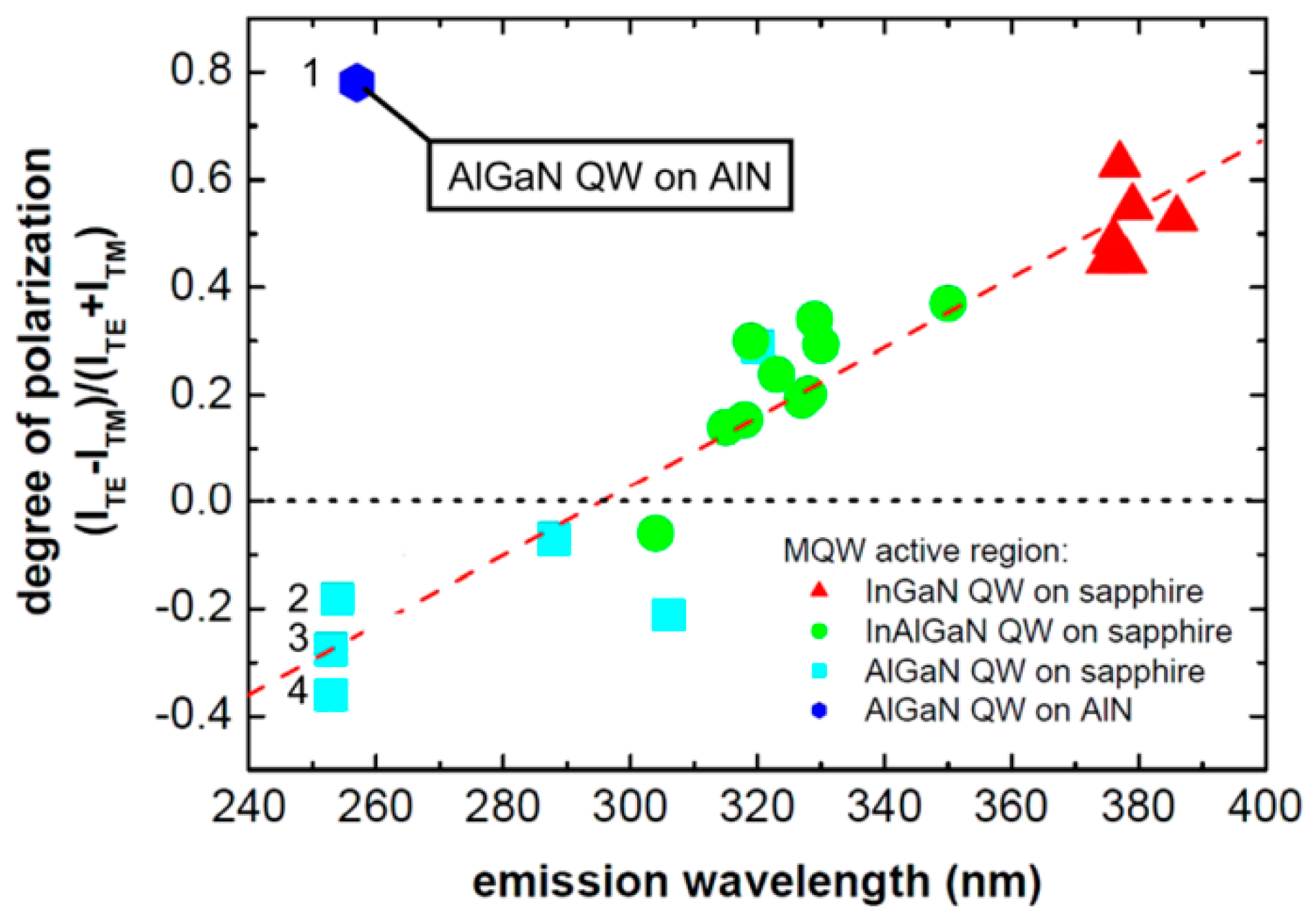
  90. Kawanishi, H.; Senuma, M.; Nukui, T. Anisotropic polarization characteristics of lasing and spontaneous surface and edge emissions from deep-ultraviolet (λ ≈ 240 nm) AlGaN multiple-quantum-well lasers. Appl. Phys. Lett. 2006, 89, 041126. [Google Scholar] [CrossRef]
  91. Sharma, T.K.; Naveh, D.; Towe, E. Strain-driven light-polarization switching in deep ultraviolet nitride emitters. Phys. Rev. B 2011, 84, 035305. [Google Scholar] [CrossRef]
  92. Northrup, J.E.; Chua, C.L.; Yang, Z.; Wunderer, T.; Kneissl, M.; Johnson, N.M.; Kolbe, T. Effect of strain and barrier composition on the polarization of light emission from AlGaN/AlN quantum wells. Appl. Phys. Lett. 2012, 100, 021101. [Google Scholar] [CrossRef]
  93. Reich, C.; Guttmann, M.; Feneberg, M.; Wernicke, T.; Mehnke, F.; Kuhn, C.; Rass, J.; Lapeyrade, M.; Einfeldt, S.; Knauer, A.; et al. Strongly transverse-electric-polarized emission from deep ultraviolet AlGaN quantum well light emitting diodes. Appl. Phys. Lett. 2015, 107, 142101. [Google Scholar] [CrossRef]
  94. Raghothamachar, B.; Vetter, W.M.; Dudley, M.; Dalmau, R.; Schlesser, R.; Sitar, Z.; Michaels, E.; Kolis, J.W. Synchrotron white beam topography characterization of physical vapor transport grown AlN and ammonothermal GaN. J. Cryst. Growth 2002, 246, 271–280. [Google Scholar] [CrossRef]
  95. Zhang, J.P.; Wang, H.M.; Gaevski, M.E.; Chen, C.Q.; Fareed, Q.; Yang, J.W.; Simin, G.; Khan, M.A. Crack-free thick AlGaN grown on sapphire using AlN/AlGaN superlattices for strain management. Appl. Phys. Lett. 2002, 80, 3542–3544. [Google Scholar] [CrossRef]
  96. Wang, H.-M.; Zhang, J.-P.; Chen, C.-Q.; Fareed, Q.; Yang, J.-W.; Khan, M.A. AlN/AlGaN superlattices as dislocation filter for low-threading-dislocation thick AlGaN layers on sapphire. Appl. Phys. Lett. 2002, 81, 604–606. [Google Scholar] [CrossRef]
  97. Xi, Y.A.; Chen, K.X.; Mont, F.; Kim, J.K.; Schubert, E.F.; Liu, W.; Li, X.; Smart, J.A. Comparative study of n-type AlGaN grown on sapphire by using a superlattice layer and a low-temperature AlN interlayer. J. Cryst. Growth 2007, 299, 59–62. [Google Scholar] [CrossRef]
  98. Chitnis, A.; Zhang, J.P.; Adivarahan, V.; Shatalov, M.; Wu, S.; Pachipulusu, R.; Mandavilli, V.; Khan, M.A. Improved performance of 325-nm emission AlGaN ultraviolet light-emitting diodes. Appl. Phys. Lett. 2003, 82, 2565–2567. [Google Scholar] [CrossRef]
  99. Nakarmi, M.; Kim, K.; Khizar, M.; Fan, Z.; Lin, J.; Jiang, H. Electrical and optical properties of Mg-doped Al0.7 Ga0.3N alloys. Appl. Phys. Lett. 2005, 86, 092108. [Google Scholar] [CrossRef]
  100. Taniyasu, Y.; Kasu, M.; Makimoto, T. An aluminium nitride light-emitting diode with a wavelength of 210 nanometres. Nature 2006, 441, 325–328. [Google Scholar] [CrossRef] [PubMed]
  101. Nam, K.B.; Nakarmi, M.L.; Li, J.; Lin, J.Y.; Jiang, H.X. Mg acceptor level in AlN probed by deep ultraviolet photoluminescence. Appl. Phys. Lett. 2003, 83, 878–880. [Google Scholar] [CrossRef]
  102. Aoyagi, Y.; Takeuchi, M.; Iwai, S.; Hirayama, H. High hole carrier concentration realized by alternative co-doping technique in metal organic chemical vapor deposition. Appl. Phys. Lett. 2011, 99, 112110. [Google Scholar] [CrossRef]
  103. Korotkov, R.; Gregie, J.; Wessels, B. Electrical properties of p-type GaN: Mg codoped with oxygen. Appl. Phys. Lett. 2001, 78, 222–224. [Google Scholar] [CrossRef]
  104. Chen, Y.; Wu, H.; Han, E.; Yue, G.; Chen, Z.; Wu, Z.; Wang, G.; Jiang, H. High hole concentration in p-type AlGaN by indium-surfactant-assisted Mg-delta doping. Appl. Phys. Lett. 2015, 106, 162102. [Google Scholar] [CrossRef]
  105. Nakarmi, M.L.; Kim, K.H.; Li, J.; Lin, J.Y.; Jiang, H.X. Enhanced p-type conduction in GaN and AlGaN by Mg-δ-doping. Appl. Phys. Lett. 2003, 82, 3041–3043. [Google Scholar] [CrossRef]
  106. Allerman, A.A.; Crawford, M.H.; Miller, M.A.; Lee, S.R. Growth and characterization of Mg-doped AlGaN–AlN short-period superlattices for deep-UV optoelectronic devices. J. Cryst. Growth 2010, 312, 756–761. [Google Scholar] [CrossRef]
  107. Cheng, B.; Choi, S.; Northrup, J.E.; Yang, Z.; Knollenberg, C.; Teepe, M.; Wunderer, T.; Chua, C.L.; Johnson, N.M. Enhanced vertical and lateral hole transport in high aluminum-containing AlGaN for deep ultraviolet light emitters. Appl. Phys. Lett. 2013, 102, 231106. [Google Scholar] [CrossRef]
  108. Kakanakova-Georgieva, A.; Nilsson, D.; Stattin, M.; Forsberg, U.; Haglund, Å.; Larsson, A.; Janzén, E. Mg-doped Al0.85Ga0.15N layers grown by hot-wall MOCVD with low resistivity at room temperature. Phys. Stat. Sol. 2010, 4, 311–313. [Google Scholar] [CrossRef]
  109. Nilsson, D. Doping of High-Al-Content AlGaN Grown by MOCVD. Ph.D. Thesis, Linköping University, Linköping, Swede, 2014. [Google Scholar]
  110. Taniyasu, Y.; Kasu, M.; Kobayashi, N. Intentional control of n-type conduction for Si-doped AlN and AlxGa1-xNwith high Al content. Phys. Stat. Sol. B 2002, 234, 845–849. [Google Scholar] [CrossRef]
  111. Taniyasu, Y.; Kasu, M.; Kobayashi, N. Intentional control of n-type conduction for Si-doped AlN and AlxGa1−xN (0.42 ≤ x < 1). Appl. Phys. Lett. 2002, 81, 1255–1257. [Google Scholar]
  112. Mehnke, F.; Wernicke, T.; Pingel, H.; Kuhn, C.; Reich, C.; Kueller, V.; Knauer, A.; Lapeyrade, M.; Weyers, M.; Kneissl, M. Highly conductive n-AlxGa1−xN layers with aluminum mole fractions above 80%. Appl. Phys. Lett. 2013, 103, 212109. [Google Scholar] [CrossRef]
Figure 1. Reported external quantum efficiencies (EQE) for group III-nitrides-based near and deep ultraviolet (DUV) light-emitting diodes (LEDs) [1,2,3,4,5,6,7,8,9,10,11,12,13,14,15,16,17,18]. In part courtesy of Prof. M. Kneissl of Technische Universität Berlin.
Crystals 07 00300 g001
Figure 2. Schematic of electron injection into multiple quantum wells (MQWs) in AlGaN-based DUV LEDs using (a) a multiple quantum barrier (MQB) and (b) a single barrier electron blocking layer (EBL). Reprinted with permission from [17]. Copyright 2014, The Japan Society of Applied Physics.
Crystals 07 00300 g002
Figure 3. External optical transmission spectra of physical vapor transport (PVT)- and hydride vapor phase epitaxy (HVPE)-AlN substrates measured at RT in air. Substrates of the same thickness and surface polish state were used. Reprinted with permission from [57]. Copyright 2012, The Japan Society of Applied Physics.
Crystals 07 00300 g003
Figure 4. Atomic force microscopy (AFM) scans (5 × 5 μm) of 0.7 μm thick AlN: nid on sapphire grown at temperatures of 1300 °C, 1400 °C, and 1500 °C. RMS values are 4 nm, 1 nm and 0.4 nm from left to right. Reprinted with permission from [59]. Copyright 2008, WILEY-VCH Verlag GmbH & Co. KGaA, Weinheim.
Crystals 07 00300 g004
Figure 5. Representative gas flow sequences for (a) AlN growth by NH3 pulse-flow method, AlGaN growth by (b) pulsed atomic layer epitaxy (PALE) and (c) migration-enhanced metal organic chemical vapor deposition (MEMOCVD) methods. Patterned after Reference [17,65,69].
Crystals 07 00300 g005
Figure 6. Cross-sectional transmission electron microscopy (TEM) micrograph of a GaN thin film grown with 5 min in situ SiNx network by MOCVD on sapphire. Reprinted from [79], with the permission of AIP publishing.
Crystals 07 00300 g006
Figure 7. Scanning electron microscope (SEM) images of (a) perspective view of the stripe-patterned AlN/Si(111) template with nominally 3 µm ridges and 3 µm trenches (6 µm period) and (b) cross-sectional view of the ELO AlN layer on the patterned template. The patterning stripe is along [101 1 ¯ 0] AlN. Reprinted from [85], with the permission of AIP publishing.
Crystals 07 00300 g007
Figure 8. Degree of polarization of emission from LEDs fabricated on sapphire or AlN substrates. For the devices grown on sapphire, TE polarization is obtained at wavelengths greater than ~310 nm and TM polarization is obtained for wavelengths less than ~310 nm. Device 1, in the upper left hand corner represents a different approach in that its active region consisting of short period AlGaN/AlGaN quantum wells was pseudomorphically grown on AlN. As depicted, it emits highly TE polarized light at 253 nm. The quantum wells in Devices 2–4 (cyan colored squares) are identical in design to Device 1 but are grown on sapphire. The long dashed line is intended to illustrate the trend for LEDs grown on sapphire while the horizontal dotted line depicts the case of equally split polarization. Reprinted from [92], with the permission of AIP publishing.
Crystals 07 00300 g008
Figure 9. Schematic of UV LED structures with a transparent p-type AlGaN: Mg contact layer and a Rh mirror electrode. After Reference [8].
Crystals 07 00300 g009
Figure 10. Schematic of the band structure of an Mg-doped AlxGa1-xN/AlyGa1-yN (x < y) superlattice. The dashed red line represents the Fermi energy; the empty circles represent the energy of the Mg acceptor when ionized, and the blue solid circles represent the accumulation of holes at the heterointerfaces.
Crystals 07 00300 g010
Table 1. Lattice parameters and properties of substrate materials for growth of deep ultraviolet light-emitting diodes (DUV LEDs) [33,34]. Mismatch calculations for sapphire take into account the 30 degree in-plane rotation.
Substratea-Axis (Å)c-Axis ÅMismatch to GaNMismatch to AlNThermal conductivity (W/cm K)UV transparencyAvailabilityPrice
Sapphire4.76512.98216.1%13.3%0.23√√√√√√
Si (111)3.8403.13617%19%1.6X√√√√
6H-SiC3.07315.1173.8%1.3%4.9XX
4H-SiC3.07610.0533.7%1.2%3.7XX
GaN3.1895.1860%2.4%3.2XXXX
AlN3.1124.9822.5%0%2.1XXXXX

