
Recent Progress in Computational Materials Science for Semiconductor Epitaxial Growth


Abstract
:
1. Introduction
2. Computational Methods
3. Hetero-Epitaxial Growth of InAs on GaAs
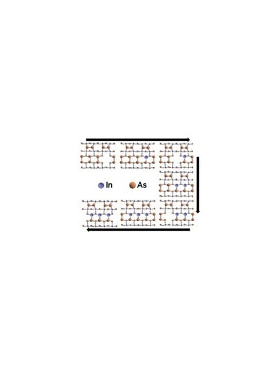
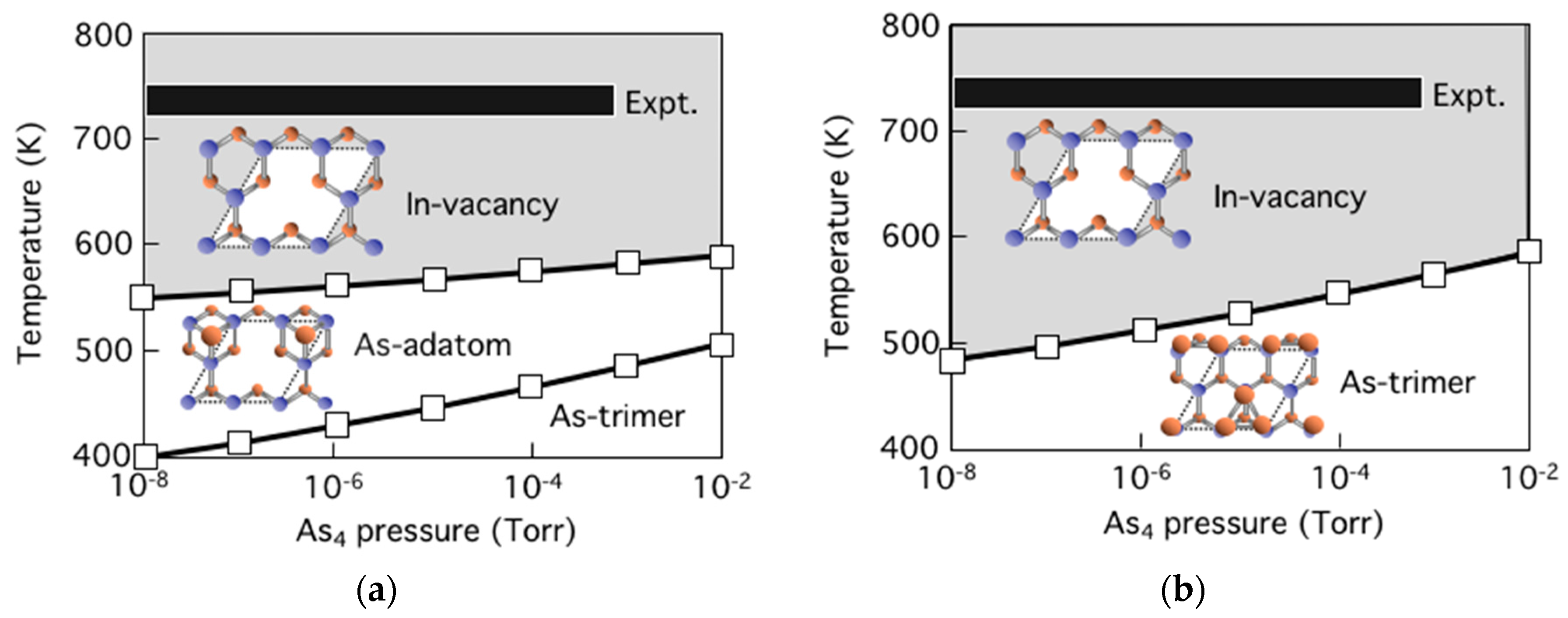
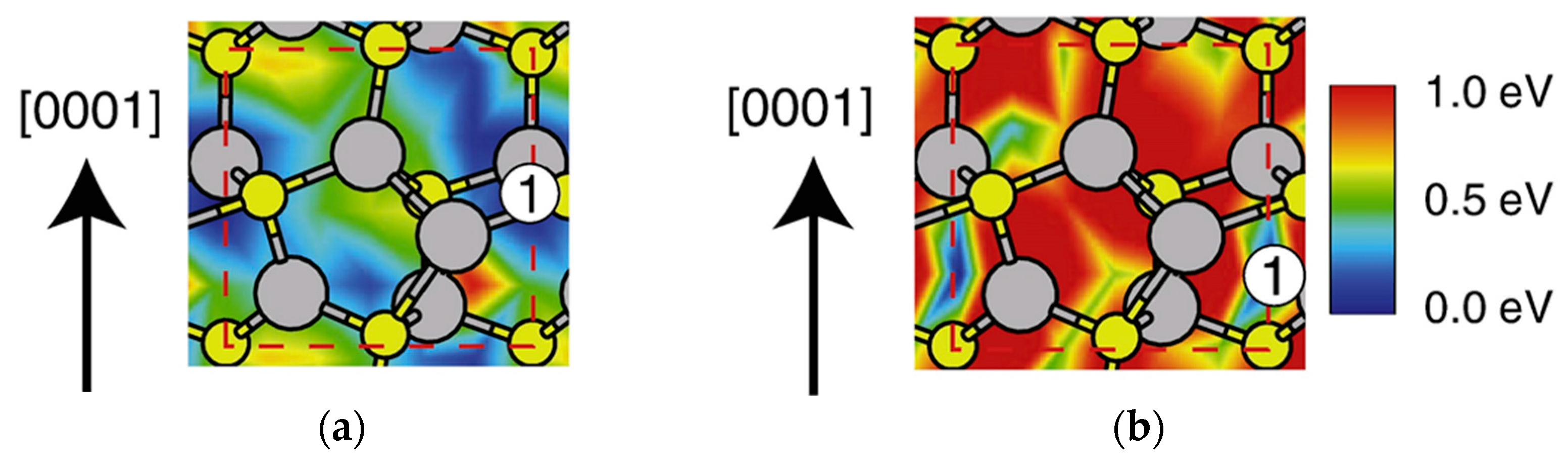
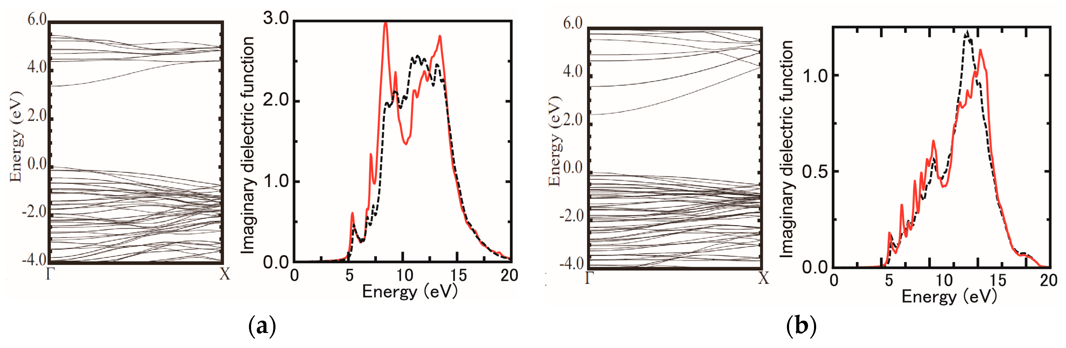
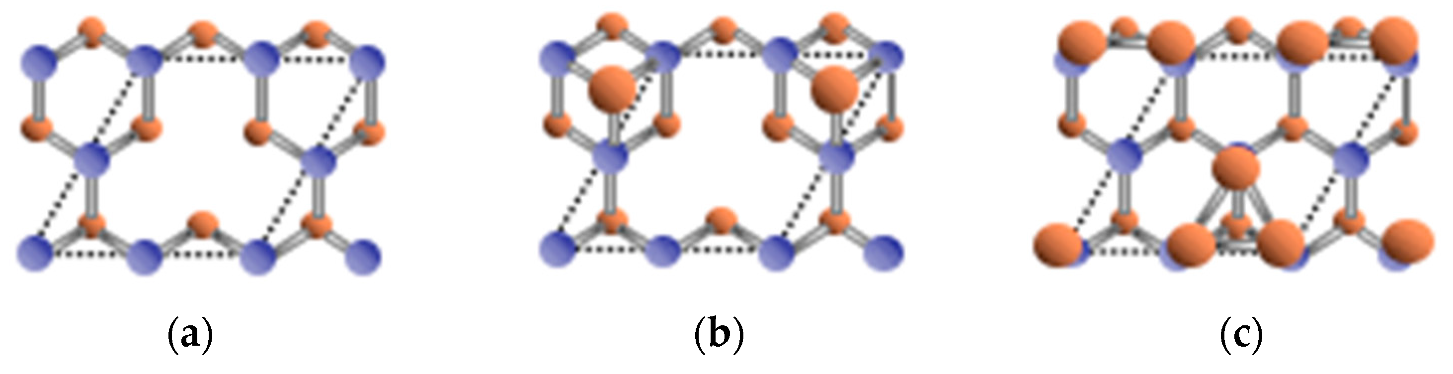
3.1. Surface Reconstructions on InAs(111)A WL
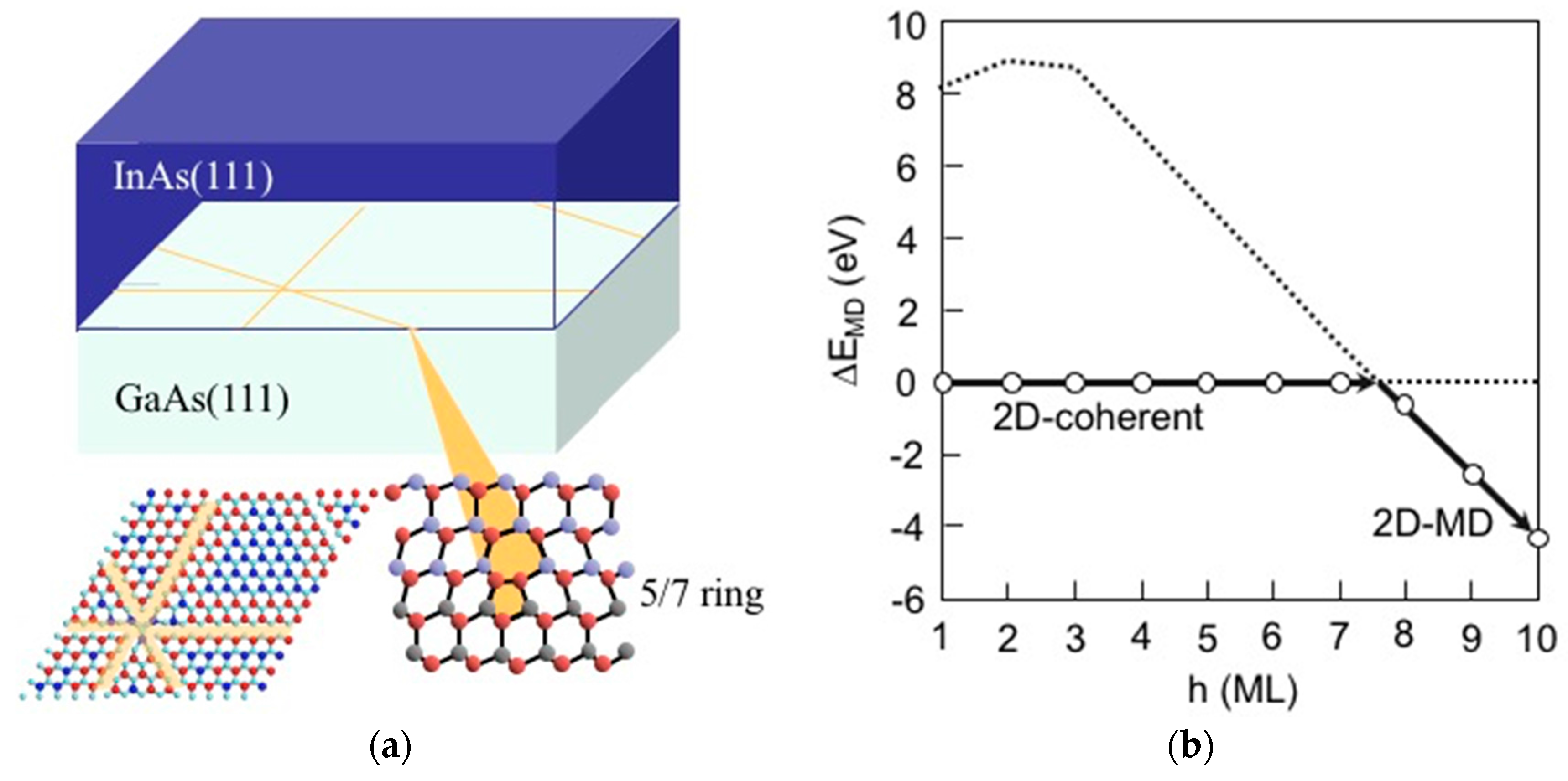
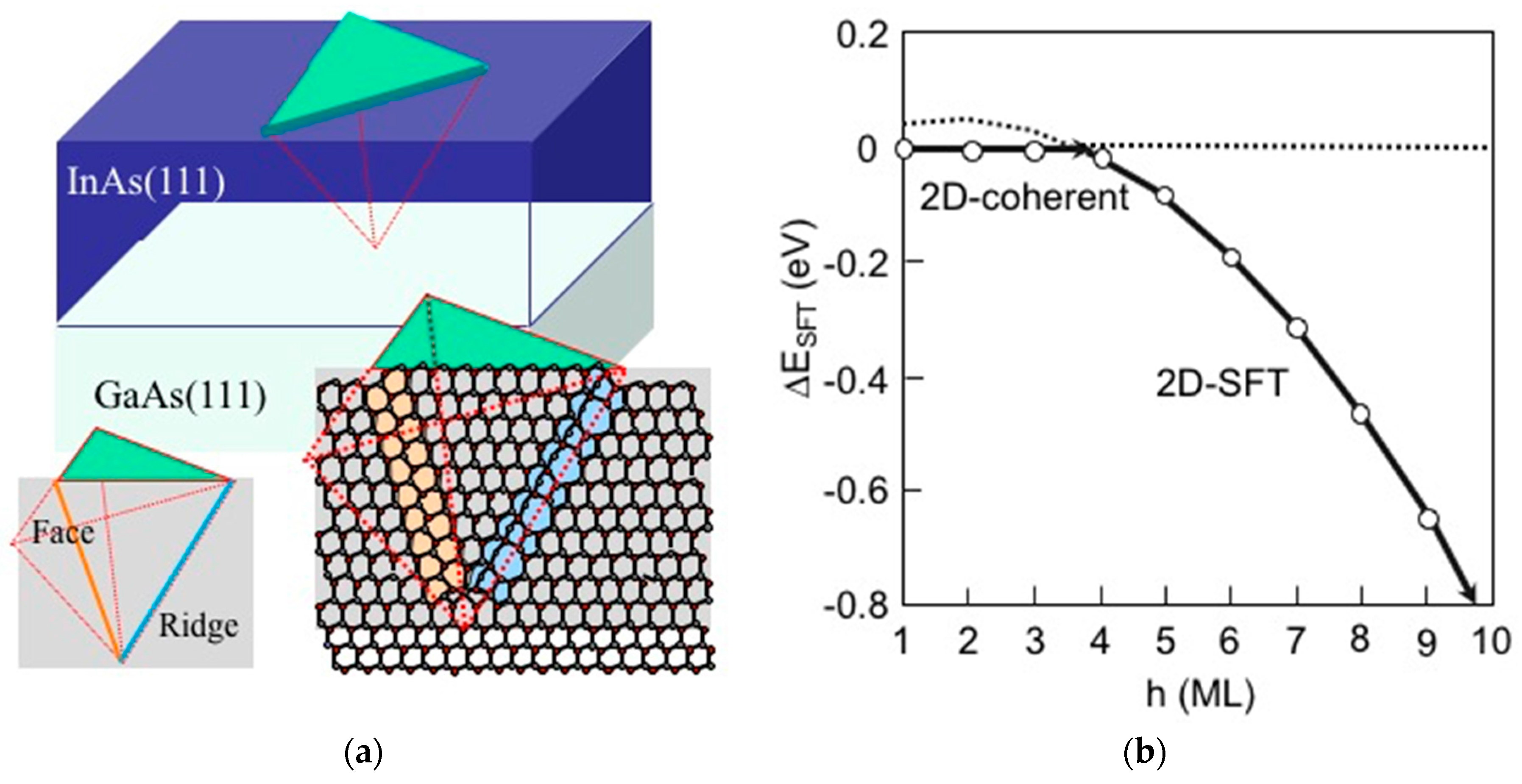
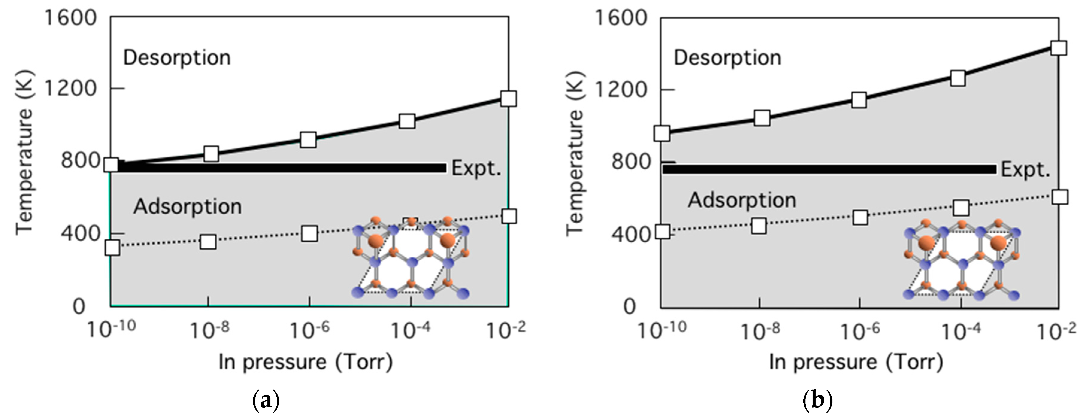
3.2. Growth Process on InAs(111)A WL
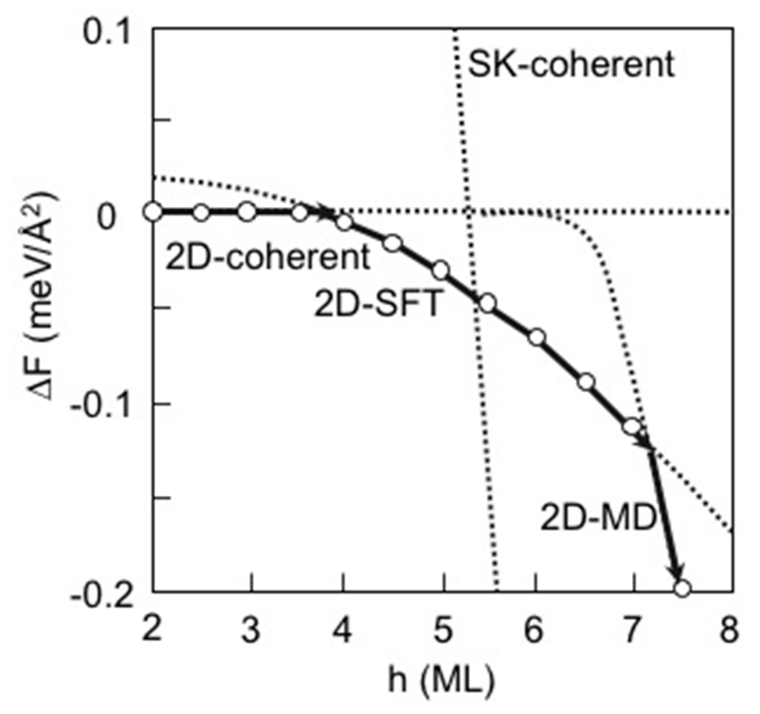
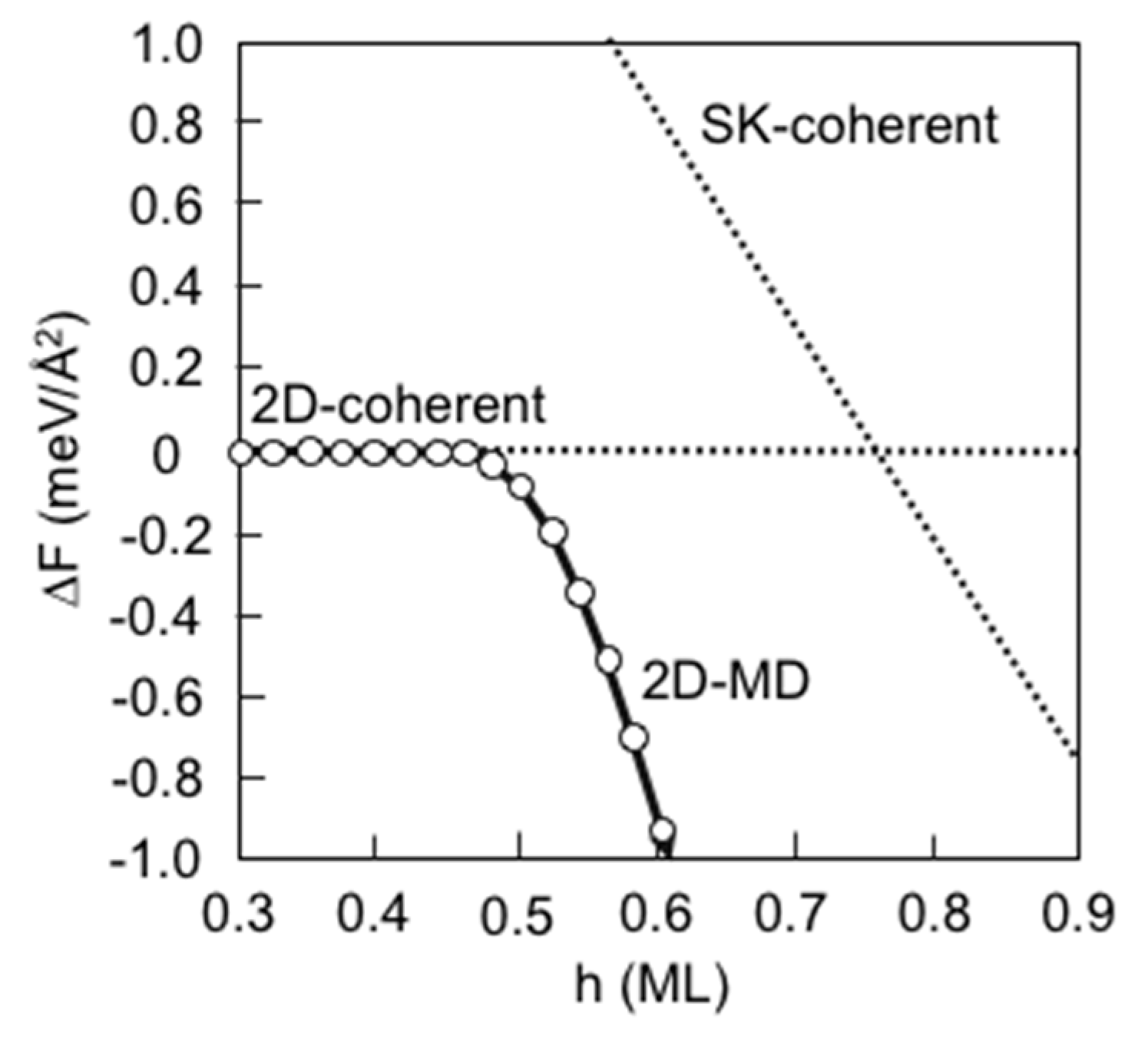
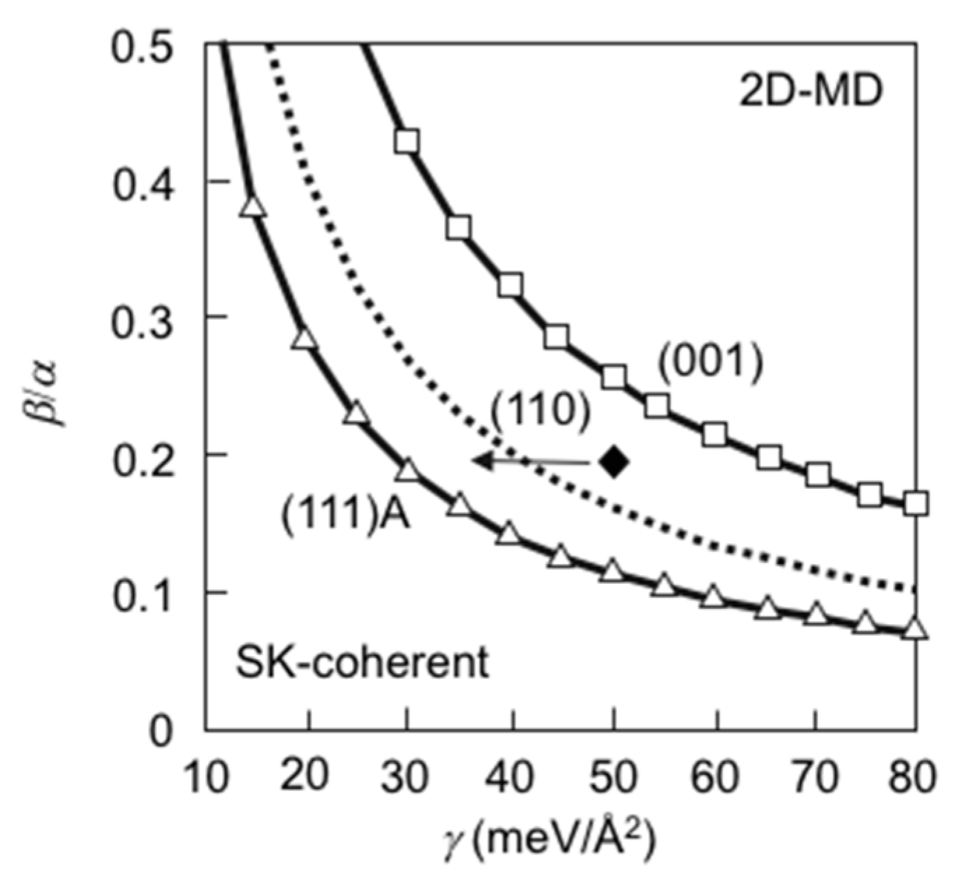
3.3. Strain Relaxation on InAs(111)A WL
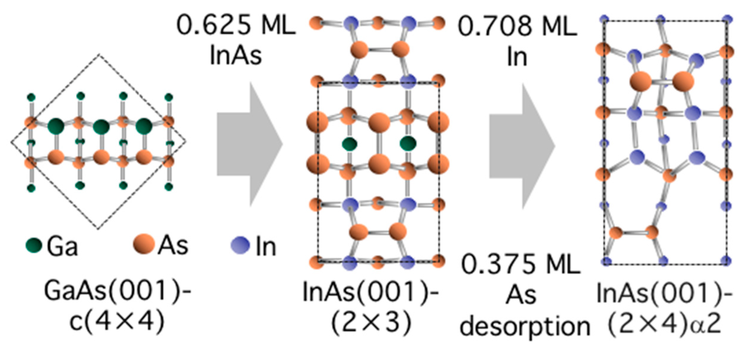
3.4. Hetero-Epitaxial Growth of InAs on GaAs(111)A
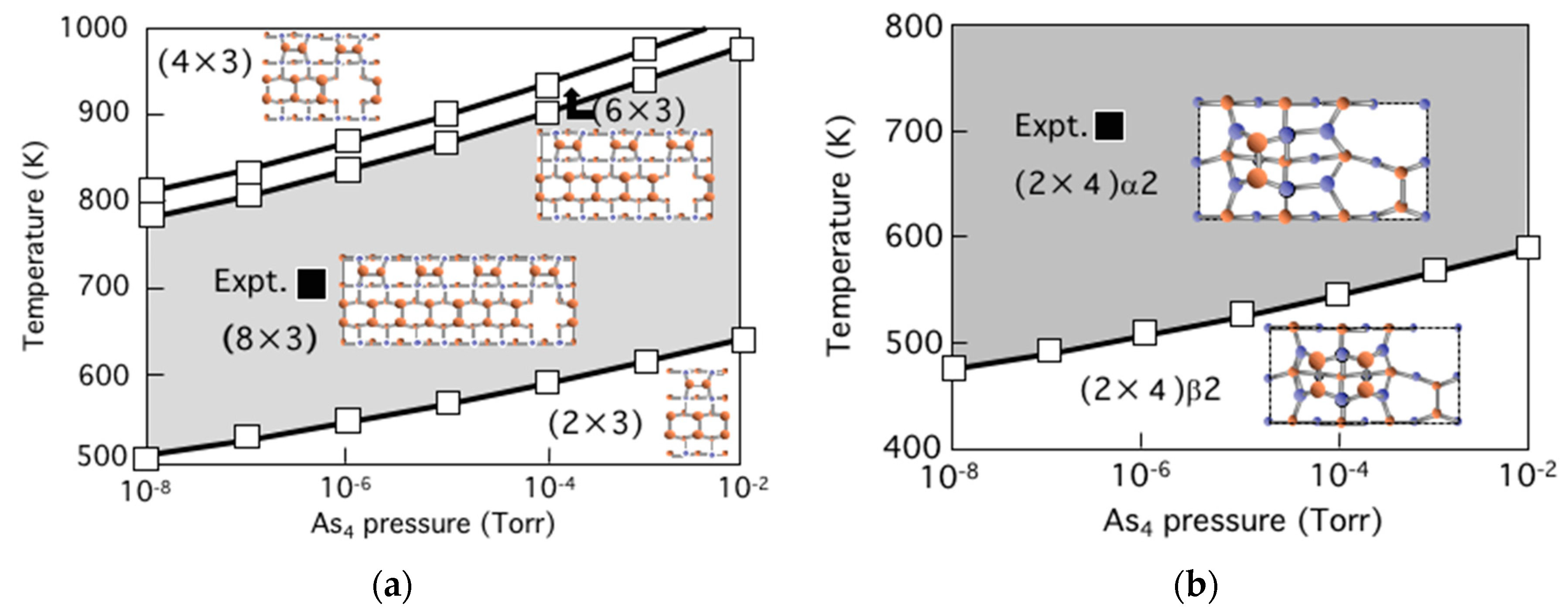
3.5. Surface Reconstructions on InAs(001) WL
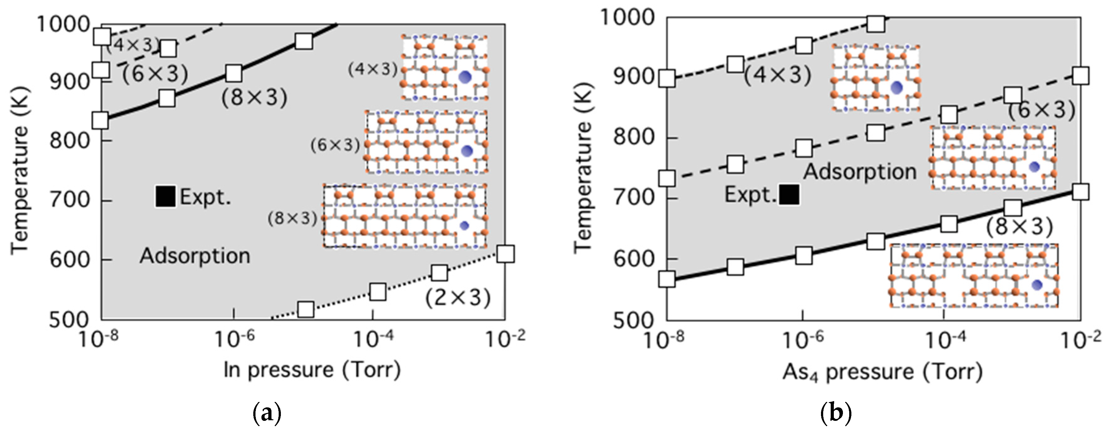
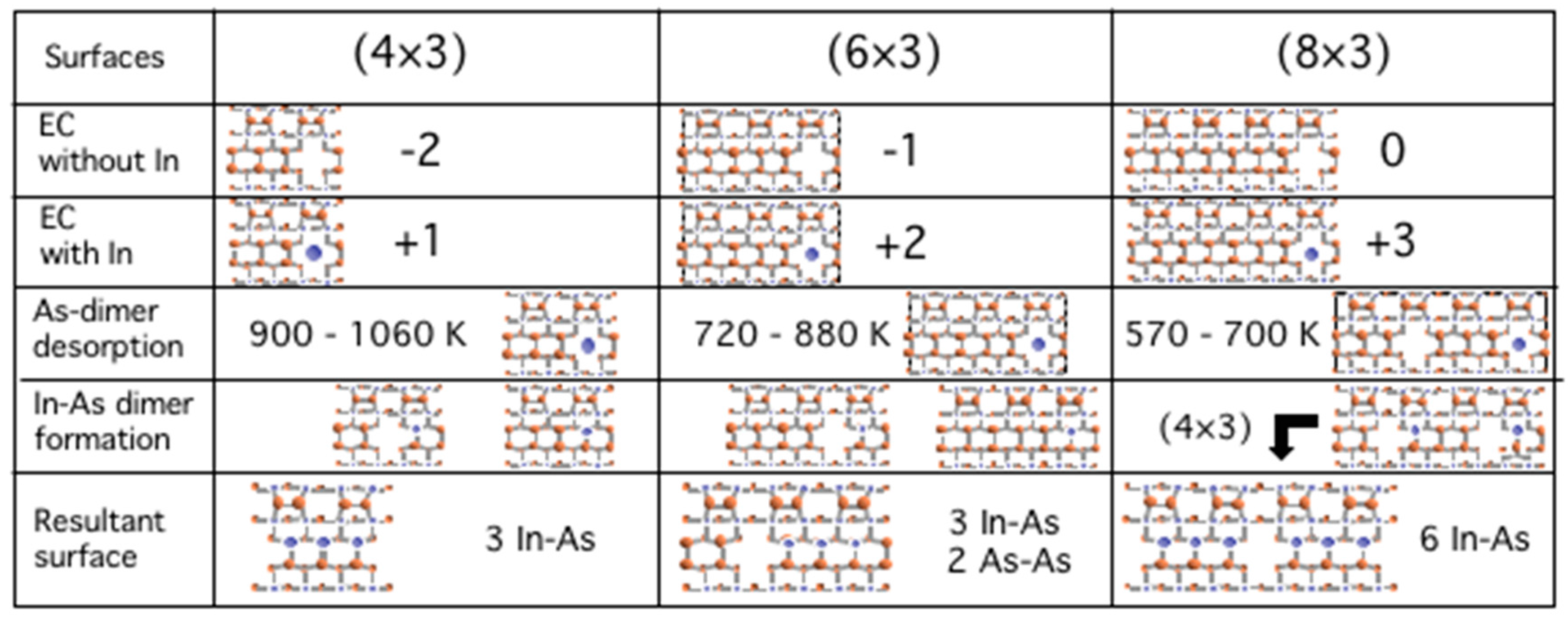
3.6. Growth Process on InAs(001) WL
3.7. Strain Relaxation on InAs(001) WL
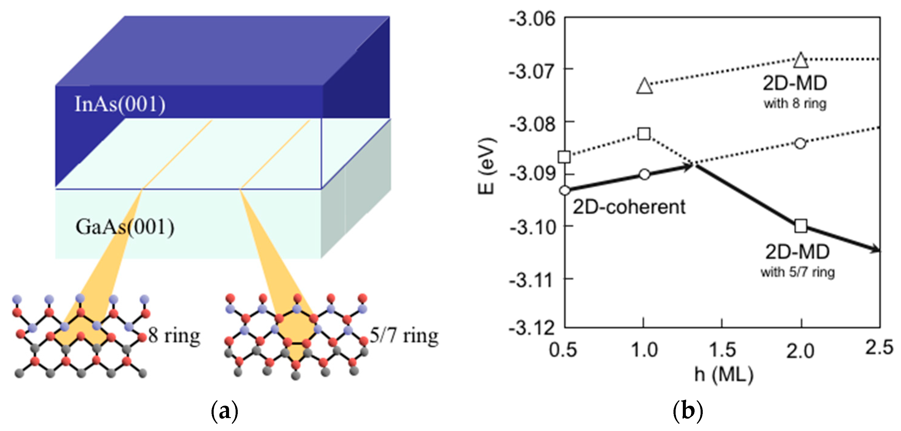
3.8. Hetero-Epitaxial Growth of InAs on GaAs(001)
3.9. Quantum Dot Formation of InAs
4. Growth Processes of InP NWs
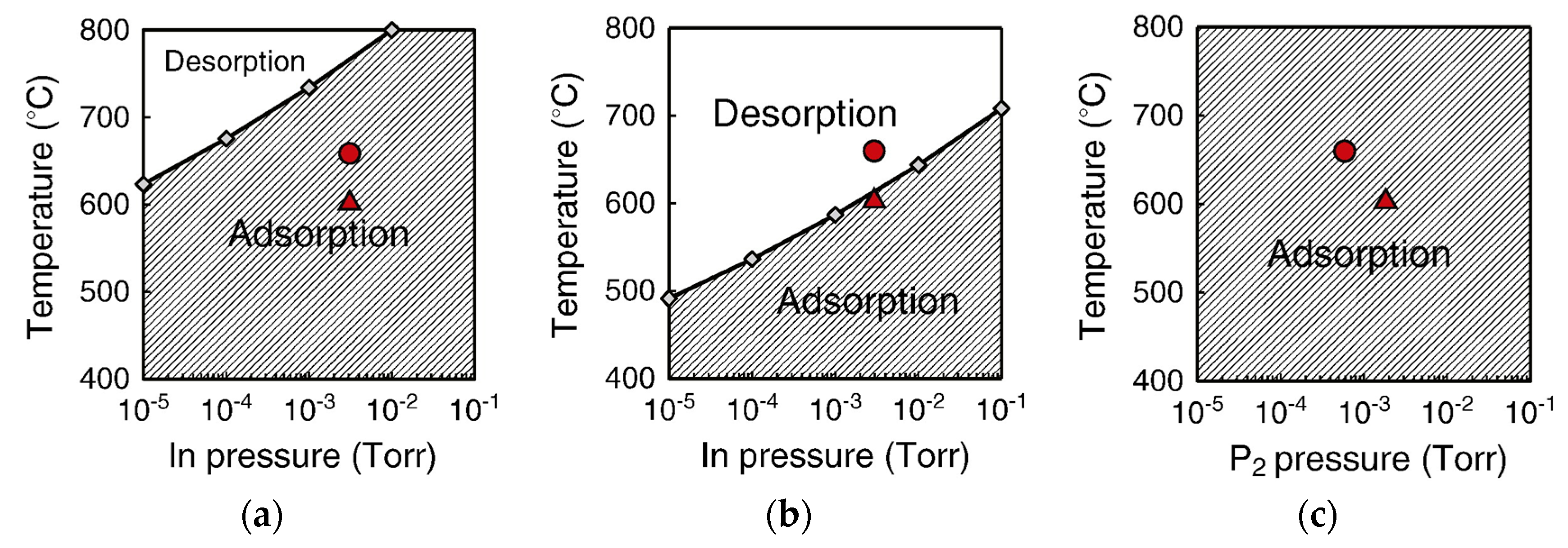
4.1. Nanowire Growth on the Basis of Classical Nucleaton Theory
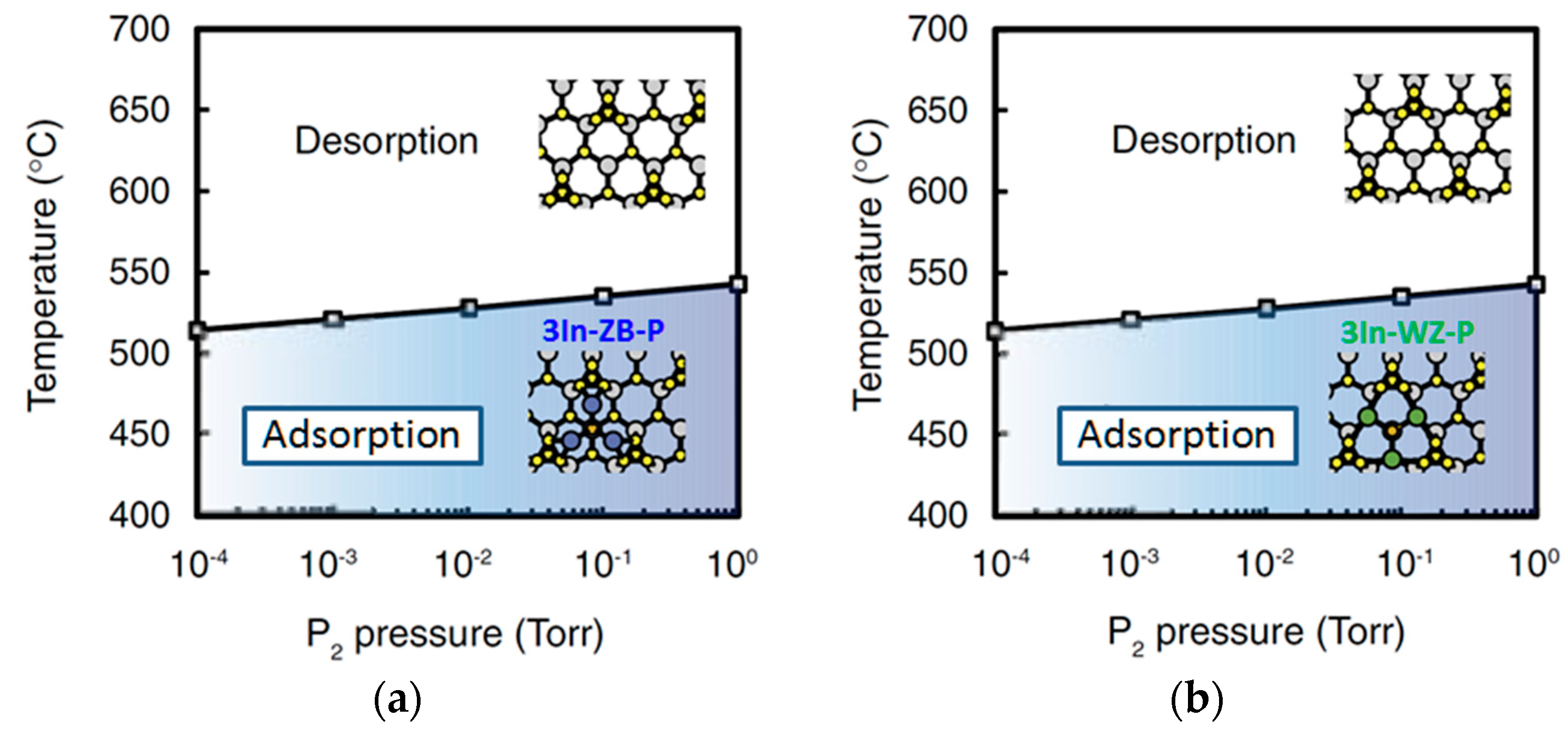
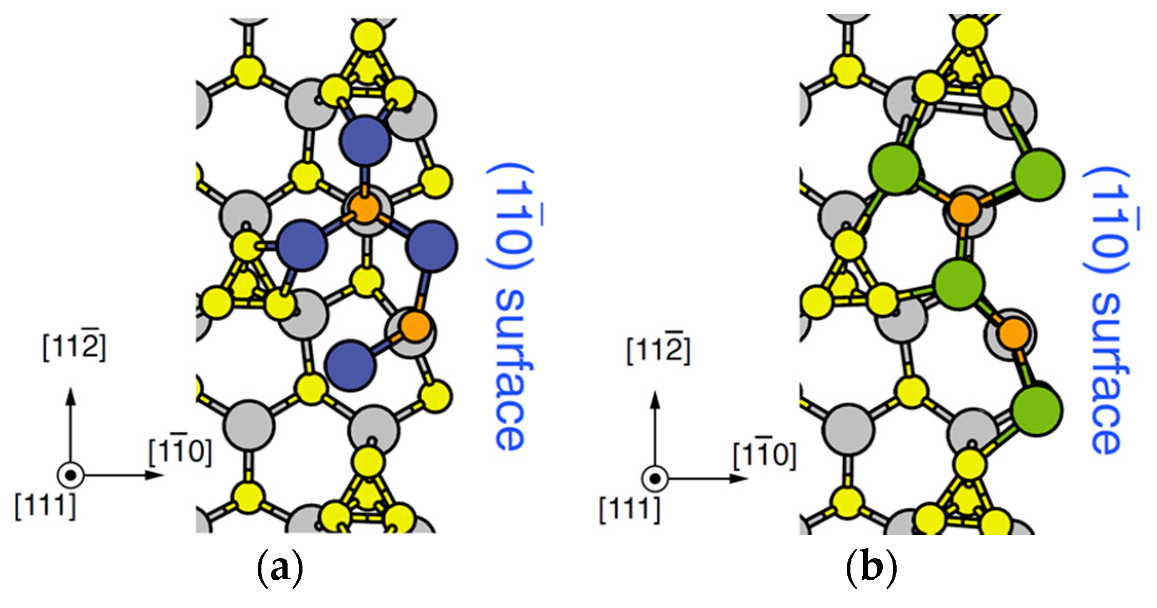
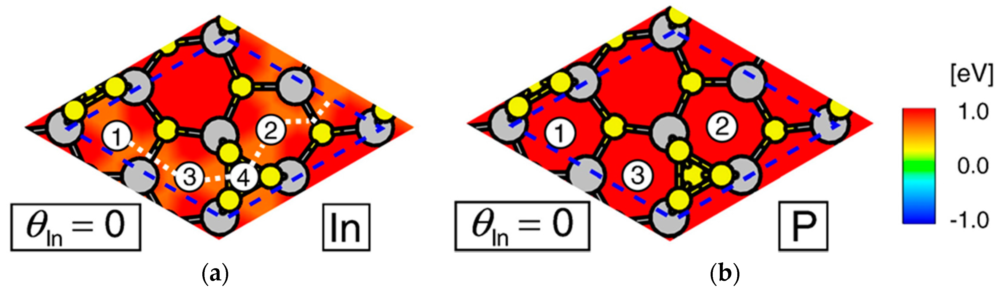
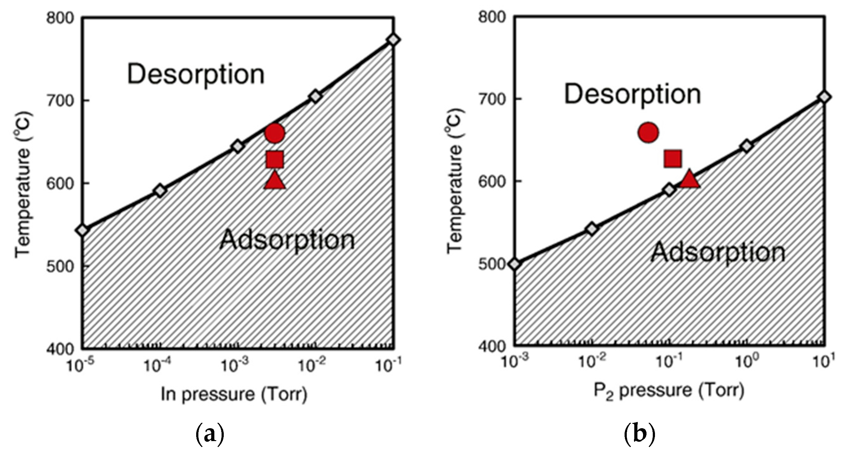
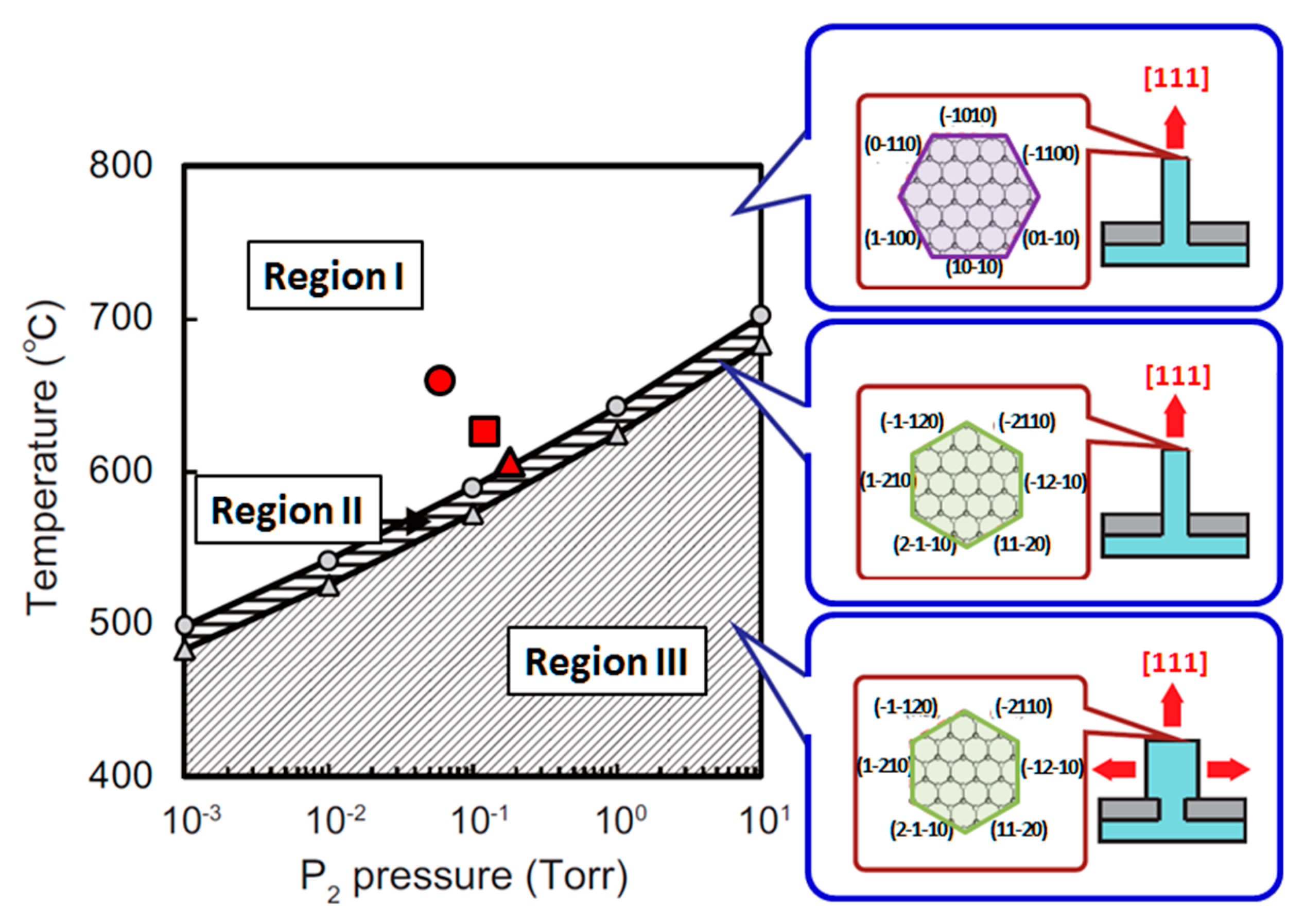
4.2. Effect of Side Facets on Adsorption–Desorption Behaviors at Top Layers in InP NWs
4.3. Nanowire Growth Processes under Epitaxial Growth Condirions
4.4. Effects of Growth Condition on InP NW Shape
5. Concluding Remarks
Acknowledgments
Author Contributions
Conflicts of Interest
References
- Däweritz, L.; Hey, R. Reconstruction and defect structure of vicinal GaAs(001) and AlxGa1-xAs surfaces during MBE growth. Surf. Sci. 1990, 236, 15–22. [Google Scholar] [CrossRef]
- Kaxiras, E.; Bar-Yam, Y.; Joannopoulos, J.D.; Pandey, K.C. Ab initio theory of polar semiconductor surfaces. I. Methodology and the (2 × 2) reconstructions of GaAs(111). Phys. Rev. B 1987, 35, 9625–9635. [Google Scholar] [CrossRef]
- Qian, G.X.; Martin, R.M.; Chadi, D.J. Stoichiometry and surface reconstruction: An ab initio study of GaAs(001) surfaces. Phys. Rev. Lett. 1988, 60, 1962–1965. [Google Scholar] [CrossRef] [PubMed]
- Northrup, J.E. Structure of Si(100)H: Dependence on the H chemical potential. Phys. Rev. B 1991, 44, 1419–1422. [Google Scholar] [CrossRef]
- Kangawa, Y.; Ito, T.; Taguchi, A.; Shiraishi, K.; Ohachi, T. A new theoretical approach to adsorption-desorption behavior of Ga on GaAs surfaces. Surf. Sci. 2001, 493, 178–181. [Google Scholar] [CrossRef]
- Kangawa, Y.; Ito, T.; Hiraoka, Y.S.; Taguchi, A.; Shiraishi, K.; Ohachi, T. Theoretical approach to influence of As2 pressure on GaAs growth kinetics. Surf. Sci. 2002, 507, 285–289. [Google Scholar] [CrossRef]
- Ito, T.; Akiyama, T.; Nakamura, K. Ab initio-based approach to reconstruction, adsorption and incorporation on GaN surfaces. Semicond. Sci. Technol. 2012, 27, 024010. [Google Scholar] [CrossRef]
- Kangawa, Y.; Akiyama, T.; Ito, T.; Shiraishi, K.; Nakayama, T. Surface stability and growth kinetics of compound semiconductors: An ab initio-based approach. Materials 2013, 6, 3309–3360. [Google Scholar] [CrossRef]
- Ito, T.; Kangawa, Y. Ab Initio-Based Approach to Crystal Growth: Chemical Potential Analysis. In Handbook of Crystal Growth, 2nd ed.; Nishinaga, T., Rudolph, P., Kuech, T.F., Eds.; Elsevier: Amsterdam, The Netherlands, 2015; Volume IA, pp. 477–520. [Google Scholar]
- Perdew, J.P.; Burke, K.; Ernzerhof, M. Generalized gradient approximation made simple. Phys. Rev. Lett. 1997, 77, 3865–3868. [Google Scholar] [CrossRef] [PubMed]
- Louie, S.G.; Froyen, S.; Cohen, M.L. Nonlinear ionic pseudopotentials in spin-density-functional calculations. Phys. Rev. B 1982, 26, 1738–1742. [Google Scholar] [CrossRef]
- Yamauchi, J.; Tsukada, M.; Watanabe, S.; Sugino, O. First-principles study on energetics of c-BN(001) reconstructed surfaces. Phys. Rev. B 1996, 54, 5586–5603. [Google Scholar] [CrossRef]
- Shiraishi, K. A new slab model approach for electronic structure calculation of polar semiconductor surface. J. Phys. Soc. Jpn. 1990, 59, 3455–3458. [Google Scholar] [CrossRef]
- Shiraishi, K.; Oyama, N.; Okajima, K.; Miyagishima, N.; Takeda, K.; Yamaguchi, H.; Ito, T.; Ohno, T. First principles and macroscopic theories of semiconductor epitaxial growth. J. Cryst. Growth 2002, 237–239, 206–211. [Google Scholar] [CrossRef]
- Khor, K.E.; das Sarma, S. Proposed universal interatomic potential for elemental tetrahedrally bonded semiconductors. Phys. Rev. B 1988, 38, 3318–3822. [Google Scholar] [CrossRef]
- Ito, T.; Khor, K.E.; das Sarma, S. Systematic approach to developing empirical potentials for compound semiconductors. Phys. Rev. B 1990, 41, 3893–3896. [Google Scholar] [CrossRef]
- Ito, T. Simple criterion for wurtzite-zinc-blende polytypism in semiconductors. Jpn. J. Appl. Phys. 1998, 37, L1217–L1220. [Google Scholar] [CrossRef]
- Kangawa, Y.; Ito, T.; Taguchi, A.; Shiraishi, K.; Irisawa, T.; Ohachi, T. Monte Carlo simulation for temperature dependence of Ga diffusion length on GaAs(001). Appl. Surf. Sci. 2002, 190, 517–520. [Google Scholar] [CrossRef]
- Itoh, M.; Bell, G.R.; Avery, A.R.; Jones, T.S.; Joyce, B.A.; Vvedensky, D.D. Island nucleation and growth on reconstructed GaAs(001) surfaces. Phys. Rev. Lett. 1998, 81, 633–636. [Google Scholar] [CrossRef]
- Joyce, B.A.; Sudijono, J.L.; Belk, J.G.; Yamaguchi, H.; Zhang, X.M.; Dobbs, H.T.; Zangwill, A.; Vvedensky, D.D.; Jones, T.S. A scanning tunneling microscopy-reflection high energy electron diffraction-rate equation study of the molecular beam epitaxial growth of InAs on GaAs(001), (110) and (111)A-quantum dots and two-dimensional modes. Jpn. J. Appl. Phys. 1997, 36, 4111–4117. [Google Scholar] [CrossRef]
- Yamaguchi, H.; Belk, J.G.; Zhang, X.M.; Sudijono, J.L.; Fay, M.R.; Jones, T.S.; Pashley, D.W.; Joyce, B.A. Atomic-scale imaging of strain relaxation via misfit dislocation in highly mismatched semiconductor heteroepitaxy: InAs/GaAs(111)A. Phys. Rev. B 1997, 55, 1337–1340. [Google Scholar] [CrossRef]
- Ohtake, A.; Ozeki, M. Strain relaxation in InAs/GaAs(111)A heteroepitaxy. Phys. Rev. Lett. 2000, 84, 4665–4668. [Google Scholar] [CrossRef] [PubMed]
- Zepeda-Ruiz, L.A.; Maroudas, D.; Weinberg, W.H. Semicoherent interface formation and structure in InAs/GaAs(111)A heteroepitaxy. Surf. Sci. 1998, 418, L68–L72. [Google Scholar] [CrossRef]
- Joe, H.; Akiyama, T.; Nakamura, K.; Kanisawa, K.; Ito, T. An empirical potential approach to the structural stability of InAs stacking-fault tetrahedron in InAs/GaAs(111). J. Cryst. Growth 2007, 301–302, 837–840. [Google Scholar] [CrossRef]
- Taguchi, A.; Kanisawa, K. Stable reconstruction and adsorbates of InAs(111)A surface. Appl. Surf. Sci. 2006, 252, 5263–5266. [Google Scholar] [CrossRef]
- Belk, J.G.; McConville, C.F.; Sudijono, J.L.; Jones, T.S.; Joyce, B.A. Surface alloying at InAs/GaAs interfaces grown on (001) surfaces by molecular beam epitaxy. Surf. Sci. 1997, 387, 213–226. [Google Scholar] [CrossRef]
- Grabowski, J.; Prohl, C.; Höpfner, B.; Dähne, M.; EIsele, H. Evolution of the InAs wetting layer on GaAs(001)-c(4 × 4) on the atomic scale. Appl. Phys. Lett. 2009, 95, 233118. [Google Scholar] [CrossRef]
- Eisele, H.; Höpfner, B.; Prohl, C.; Grabowski, J.; Dähne, M. Atomic structure of the (4 × 3) reconstructed InGaAs monolayer on GaAs(001). Surf. Sci. 2010, 604, 283–289. [Google Scholar] [CrossRef]
- Konishi, T.; Tsukamoto, S. Statistical analysis of surface reconstruction domains on InAs wetting layer preceding quantum dot formation. Nanoscale Res. Lett. 2010, 5, 1901–1904. [Google Scholar] [CrossRef] [PubMed]
- Kratzer, P.; Penev, E.; Scheffler, M. Understanding the growth mechanisms of GaAs and InGaAs thin films by employing first-principles calculations. Appl. Surf. Sci. 2003, 216, 436–446. [Google Scholar] [CrossRef]
- Ito, T.; Ishimure, N.; Akiyama, T.; Nakamura, K. Ab initio-based approach to adsorption-desorption behavior on the InAs(111)A heteroepitaxially grown on GaAs substrate. J. Cryst. Growth 2011, 318, 72–75. [Google Scholar] [CrossRef]
- Ito, T.; Ogasawara, K.; Sugitani, T.; Akiyama, T.; Nakamura, K. Ab initio-based approach to elemental growth process on the InAs wetting layer grown on GaAs substrate. J. Cryst. Growth 2013, 362, 2–5. [Google Scholar] [CrossRef]
- Ito, T.; Hirai, K.; Akiyama, T.; Nakamura, K. Ab initio-based approach to novel behavior of InAs wetting layer grown on GaAs(001). J. Cryst. Growth 2013, 378, 13–16. [Google Scholar] [CrossRef]
- Ito, T.; Akiyama, T.; Nakamura, K. Ab initio-based approach to structural change in InAs(001)-(2 × 3) wetting layer surfaces during MBE growth. e-J. Surf. Sci. Nanotechnol. 2015, 13, 190–194. [Google Scholar] [CrossRef]
- Yamaguchi, H.; Homma, Y.; kanisawa, K.; Hirayama, H. Drastic improvement in surface flatness properties by using GaAs(111)A substrates in molecular beam epitaxy. Jpn. J. Appl. Phys. 1999, 38, 635–644. [Google Scholar] [CrossRef]
- Yamaguchi, H.; Sudijiono, J.L.; Joyce, B.A.; Jones, T.S.; Gatzke, C.; Stradling, R.A. Thickness-dependent electron accumulation in InAs thin films on GaAs(111)A: A scanning tunneling-spectroscopy study. Phys. Rev. B 1998, 58, 4219–4222. [Google Scholar] [CrossRef]
- Phillips, J.C. Ionicity of the chemical bond in crystals. Rev. Mod. Phys. 1970, 42, 317–356. [Google Scholar] [CrossRef]
- Farrell, H.H.; Harbison, J.P.; Peterson, L.D. Molecular-beam epitaxy growth mechanisms on GaAs(100) surfaces. J. Vac. Sci. Technol. B 1987, 5, 1482–1489. [Google Scholar] [CrossRef]
- Pashley, M.D. Electron counting model and its application to island structures on molecular-beam epitaxy grown on GaAs(001) and ZnSe(001). Phys. Rev. B 1989, 40, 10481–10487. [Google Scholar] [CrossRef]
- Shiraishi, K.; Ito, T. Ga-adatom-induced As rearrangement during GaAs epitaxial growth: Self-surfactant effect. Phys. Rev. B 1998, 57, 6301–6304. [Google Scholar] [CrossRef]
- Tatematsu, H.; Sano, K.; Akiyama, T.; Nakamura, K.; Ito, T. Ab initio-based approach to initial growth processes on GaAs(111)B-(2 × 2) surfaces: Self-surfactant effect of Ga adatoms revisited. Phys. Rev. B 2008, 77, 233306-1-4. [Google Scholar] [CrossRef]
- Ito, T.; Akiyama, T.; Nakamura, K. Theoretical investigations for strain relaxation and growth mode of InAs thin layers on GaAs(111)A. Condens. Matter 2016, 1, 4. [Google Scholar] [CrossRef]
- Potin, V.; Ruterana, P.; Nouet, G.; Pond, R.C.; Morkoç, H. Mosaic growth of GaN on (0001) sapphire: A high-resolution electron microscopy and crystallographic study of threading dislocations from low-angle to high-angle grain boundaries. Phys. Rev. B 2000, 61, 5587–5589. [Google Scholar] [CrossRef]
- Ichimura, M. Stillinger-Weber potentials for III-V compound semiconductors and their application to the critical thickness calculation for InAs/GaAs. Phys. Status Solidi A 1996, 153, 431–437. [Google Scholar] [CrossRef]
- Béré, A.; Serra, A. Atomic structure of dislocation cores in GaN. Phys. Rev. B 2002, 65, 205323. [Google Scholar] [CrossRef]
- Kawamoto, K.; Suda, T.; Akiyama, T.; Nakamura, K.; Ito, T. An empirical potential approach to dislocation formation and structural stability in GaNxAs1-x. Appl. Surf. Sci. 2005, 244, 182–185. [Google Scholar] [CrossRef]
- People, B.; Bean, J.C. Calculation of critical layer thickness versus lattice mismatch for GexSi1-x/Si strained-layer heterostructures. Appl. Phys. Lett. 1985, 47, 322–324. [Google Scholar] [CrossRef]
- Kobayashi, R.; Nakayama, T. First-principles study on crystal and electronic structures of stacking-fault tetrahedron in epitaxial Si films. J. Cryst. Growth 2004, 278, 500–504. [Google Scholar] [CrossRef]
- Zhou, N.; Zhou, L. A fusion-crystalization mechanism for nucleation of misfit dislocations in FCC epitaxial films. J. Cryst. Growth 2006, 289, 681–685. [Google Scholar] [CrossRef]
- Wang, L.G.; Kratzer, P.; Moll, N.; Scheffler, M. Size, shape, and stability of InAs quantum dots on the GaAs(001) substrate. Phys. Rev. B 2000, 62, 1897–1904. [Google Scholar] [CrossRef]
- Kita, T.; Wada, O.; Nakayama, T.; Murayama, M. Optical reflectance study of the wetting layers in (In, Ga)As self-assembled quantum dot growth on GaAs(001). Phys. Rev. B 2002, 66, 195312. [Google Scholar] [CrossRef]
- Patella, F.; Nufris, S.; Arciprete, F.; Fanfoni, M.; Placidi, E.; Segarlata, A.; Balzarotti, A. Tracing the two- to three-dimensional transition in the InAs/GaAs(001) heteroepitaxial growth. Phys. Rev. B 2003, 67, 205308. [Google Scholar] [CrossRef]
- Xu, C.; Temko, Y.; Suzuki, T.; Jacobi, K. InAs wetting layer evolution on GaAs(001). Surf. Sci. 2005, 580, 30–38. [Google Scholar] [CrossRef]
- Yamaguchi, H.; Horikoshi, Y. Unified model for structure transition and electrical properties of InAs(001) surfaces studied by scanning tunneling microscopy. Jpn. J. Appl. Phys. 1994, 33, L1423–L1426. [Google Scholar] [CrossRef]
- Kaida, R.; Akiyama, T.; Nakamura, K.; Ito, T. Theoretical study for misfit dislocation formation at InAs/GaAs(001) interface. J. Cryst. Growth 2016. [Google Scholar] [CrossRef]
- Joyce, B.A.; Vvedensky, D.D. Self-organized growth on GaAs surfaces. Mater. Sci. Eng. R 2004, 46, 127–176. [Google Scholar] [CrossRef]
- Blumin, M.; Ruda, H.E.; Savelyev, I.G.; Shik, A.; Wang, H. Self-assembled InAs quantum dots and wires grown on a cleaved-edge GaAs(110) surface. J. Appl. Phys. 2006, 99, 093518. [Google Scholar] [CrossRef]
- Aierken, A.; Hakkarainen, T.; Sopanen, M.; Riikonen, J.; Sormunen, J.; Mattila, M.; Lipsanen, H. Self-assembled InAs island formation on GaAs(110) by metalorganic vapor phase epitaxy. Appl. Surf. Sci. 2008, 254, 2072–2076. [Google Scholar] [CrossRef]
- Yazawa, M.; Koguchi, M.; Muto, A.; Ozawa, M.; Hiruma, K. Effect of one monolayer of surface gold atoms on the epitaxial growth of InAs nanowhiskers. Appl. Phys. Lett. 1992, 61, 2051–2053. [Google Scholar] [CrossRef]
- Hiruma, K.; Yazawa, H.; Katuyama, T.; Ogawa, K.; Koguchi, M.; Kakibayashi, H. Growth and optical properties of nanometer-scale GaAs and InAs whiskers. J. Appl. Phys. 1995, 77, 447–462. [Google Scholar] [CrossRef]
- Li, H.; Wu, J.; Wang, Z. High-density InAs nanowires realized in situ on (100) InP. Appl. Phys. Lett. 1999, 75, 1173–1175. [Google Scholar] [CrossRef]
- Wu, Z.H.; Mei, X.Y.; Kim, D.; Blumin, M.; Ruda, H.E. Growth of Au-catalyzed ordered GaAs nanowire arrays by molecular-beam epitaxy. Appl. Phys. Lett. 2002, 81, 5177–5179. [Google Scholar] [CrossRef]
- Wu, Z.H.; Sun, M.; Mei, X.Y.; Ruda, H.E. Total reflection amorphous carbon mirrors for vacuum ultraviolet free electron lasers. Appl. Phys. Lett. 2004, 84, 657–659. [Google Scholar] [CrossRef]
- Morales, A.M.; Lieber, C.M. A Laser ablation method for the synthesis of crystalline semiconductor nanowires. Science 1998, 279, 208–211. [Google Scholar] [CrossRef] [PubMed]
- Wang, J.; Gudiksen, M.S.; Duan, X.; Cui, Y.; Lieber, C.M. Highly polarized photoluminescence and photodetection from single indium phosphide nanowires. Science 2001, 293, 1455–1457. [Google Scholar] [CrossRef] [PubMed]
- Gudiksen, M.S.; Lauhon, L.J.; Wang, J.; Smith, D.C.; Lieber, C.M. Growth of nanowire superlattice structures for nanoscale photonics and electronics. Nature 2002, 415, 617–620. [Google Scholar] [CrossRef] [PubMed]
- Duan, X.; Huang, Y.; Cui, Y.; Wang, J.; Lieber, C.M. Indium phosphide nanowires as building blocks for nanoscale electronic and optoelectronic devices. Nature 2001, 409, 66–69. [Google Scholar] [CrossRef] [PubMed]
- Goto, H.; Nosaki, K.; Tomioka, K.; Hara, S.; Hiruma, K.; Motohisa, J.; Fukui, T. Growth of core–shell InP nanowires for photovoltaic a lication by selective-area metal organic vapor phase epitaxy. Appl. Phys. Express 2009, 2, 035004. [Google Scholar] [CrossRef]
- Ohlsson, B.J.; Björk, M.T.; Magnusson, M.H.; de ert, K.; Samuelson, L.; Wallenberg, L.R. Size-, shape-, and position-controlled GaAs nano-whiskers. Appl. Phys. Lett. 2001, 79, 3335–3337. [Google Scholar] [CrossRef]
- Bhunia, S.; Kawamura, T.; Watanabe, Y.; Fujikawa, S.; Tokushima, K. Metalorganic vapor-phase epitaxial growth and characterization of vertical InP nanowires. Appl. Phys. Lett. 2003, 83, 3371–3373. [Google Scholar] [CrossRef]
- Motohisa, J.; Noborisaka, J.; Takeda, J.; Inari, M.; Fukui, T. Catalyst-free selective-area MOVPE of semiconductor nanowires on (111)B oriented substrates. J. Cryst. Growth 2004, 272, 180–185. [Google Scholar] [CrossRef]
- Li, Q.; Gong, X.; Wang, C.; Wang, J.; Ip, K.; Hark, S. Size-dependent periodically twinned ZnSe nanowires. Adv. Mater. 2004, 16, 1436–1440. [Google Scholar] [CrossRef]
- Johansson, J.; Karlsson, L.S.; Svensson, C.P.T.; Martensson, T.; Wacaser, B.A.; Deppert, K.; Samuelson, L.; Seifert, W. Structural properties of <111>B-oriented III–V nanowires. Nat. Mater. 2006, 5, 574–580. [Google Scholar] [CrossRef]
- Tomioka, K.; Motohisa, J.; Hara, S.; Fukui, T. Crystallographic Structure of InAs nanowires studied by transmission electron microscopy. Jpn. J. Appl. Phys. 2007, 46, L1102–L1104. [Google Scholar] [CrossRef]
- Tomioka, K.; Mohan, P.; Noborisaka, J.; Hara, S.; Motohisa, J.; Fukui, T. Growth of highly uniform InAs nanowire arrays by selective-area MOVPE. J. Cryst. Growth 2007, 298, 644–647. [Google Scholar] [CrossRef]
- Cornet, D.M.; Mazzetti, V.G.M.; la Pierre, R.R. Onset of stacking faults in InP nanowires grown by gas source molecular beam epitaxy. Appl. Phys. Lett. 2007, 90, 013116. [Google Scholar] [CrossRef]
- Spirkoska, D.; Arbiol, J.; Gustafsson, A.; Conesa-Boj, S.; Glas, F.; Zardo, I.; Heigoldt, M.; Gass, M.H.; Bleloch, A.L.; Estrade, S. Ga-assisted catalyst-free growth mechanism of GaAs nanowires by molecular beam epitaxy. Phys. Rev. B 2008, 77, 155326. [Google Scholar]
- Plante, M.C.; la Pierre, R.R. Au-assisted growth of GaAs nanowires by gas source molecular beam epitaxy: Tapering, sidewall faceting and crystal structure. J. Cryst. Growth 2008, 310, 356–363. [Google Scholar] [CrossRef]
- Algra, R.E.; Verheijen, M.A.; Borgström, M.T.; Feiner, L.; Immink, G.; van Enckevort, W.J.P.; Vlieg, E.; Bakkers, E.P.A.M. Twinning superlattices in indium phosphide nanowires. Nature 2008, 456, 369–372. [Google Scholar] [CrossRef] [PubMed]
- Paiman, S.; Gao, Q.; Tan, H.H.; Jagadish, C.; Pemasiri, K.; Montazeri, M.; Jackson, H.E.; Smith, L.M.; Yarrison-Rice, J.M.; Zhang, X.; et al. The effect of V/III ratio and catalyst particle size on the crystal structure and optical properties of InP nanowires. Nanotechnology 2009, 20, 225606. [Google Scholar] [CrossRef] [PubMed]
- Caroff, P.; Dick, K.A.; Johansson, J.; Messing, M.E.; Deppert, K.; Samuelson, L. Controlled polytypic and twin-plane superlattices in III–V nanowires. Nat. Nanotechnol. 2009, 4, 50–55. [Google Scholar] [CrossRef] [PubMed]
- Cantoro, M.; Brammertz, G.; Richard, O.; Bender, H.; Clemente, F.; Leys, M.; Degroote, S.; Caymax, M.; Heyns, M.; de Gendt, S. Controlled III/V nanowire growth by selective-area vapor-phase epitaxy. J. Electrochem. Soc. 2009, 156, H860–H868. [Google Scholar] [CrossRef]
- Vogel, A.T.; de Boor, J.; Wittemann, J.V.; Mensah, S.L.; Werner, P.; Schmidt, V. Fabrication of high-quality InSb nanowire arrays by chemical beam epitaxy. Cryst. Growth Des. 2011, 11, 1896–1900. [Google Scholar] [CrossRef]
- Bao, J.; Bell, D.C.; Capasso, F.; Wagner, J.B.; Måttensson, T.; Trägårdh, J.; Samuelson, L. Optical properties of rotationally twinned InP nanowire heterostructures. Nano Lett. 2008, 8, 836–841. [Google Scholar] [CrossRef] [PubMed]
- Yeh, C.-Y.; Lu, Z.W.; Froyen, S.; Zunger, A. Predictions and systematizations of the zinc-blende-wurtzite structural energies in binary octet compounds. Phys. Rev. B 1992, 45, R12130–R12133. [Google Scholar] [CrossRef]
- Akiyama, T.; Sano, K.; Nakamura, K.; Ito, T. An empirical potential a roach to wurtzite-zinc-blende polytypism in group III–V semiconductor nanowires. Jpn. J. Appl. Phys. 2006, 45, L275–L278. [Google Scholar] [CrossRef]
- Akiyama, T.; Nakamura, K.; Ito, T. Structural stability and electronic structures of InP nanowires: Role of surface dangling bonds on nanowire facets. Phys. Rev. B 2006, 73, 235308. [Google Scholar] [CrossRef]
- Glas, F.; Harmand, J.-C.; Patriarche, G. Why does wurtzite Form in nanowires of III–V zinc blende Semiconductors? Phys. Rev. Lett. 2007, 99, 146101. [Google Scholar] [CrossRef] [PubMed]
- Glas, F. A simple calculation of energy changes upon stacking fault formation or local crystalline phase transition in semiconductors. J. Appl. Phys. 2008, 104, 093520. [Google Scholar] [CrossRef]
- Mohan, P.; Motohisa, J.; Fukui, T. Controlled growth of highly uniform, axial/radial direction-defined, individually addressable InP nanowire arrays. Nanotechnology 2005, 16, 2903–2907. [Google Scholar] [CrossRef]
- Kitauchi, Y.; Kobayashi, Y.; Tomioka, K.; Hara, S.; Hiruma, K.; Fukui, T.; Motohisa, J. Structural transition in indium phosphide nanowires. Nano Lett. 2010, 10, 1699–1703. [Google Scholar] [CrossRef] [PubMed]
- Wagner, R.S.; Elis, W.C. Vapor-liquid-solid mechanism of single crystal growth. Appl. Phys. Lett. 1964, 4, 89–90. [Google Scholar] [CrossRef]
- Johansson, J.; Karlsson, L.S.; Dick, K.A.; Bolinsson, J.; Wacaser, B.A.; Deppert, K.; Samuelson, L.; Seifert, W. Effects of supersaturation on the crystal structure of gold seeded III–V nanowires. Cryst. Growth Des. 2009, 9, 766–773. [Google Scholar] [CrossRef]
- Akiyama, T.; Kondo, T.; Tatematsu, H.; Nakamura, K.; Ito, T. Ab initio approach to reconstructions of the InP(111)A surface: Role of hydrogen atoms passivating surface dangling bonds. Phys. Rev. B 2008, 78, 205318. [Google Scholar] [CrossRef]
- Yamashita, T.; Akiyama, T.; Nakamura, K.; Ito, T. Theoretical investigation of effect of side facets on adsorption–desorption behaviors of In and P atoms at top layers in InP nanowires. Jpn. J. Appl. Phys. 2011, 50, 55001. [Google Scholar] [CrossRef]
- Taguchi, A.; Shiraishi, K.; Ito, T.; Kangawa, Y. Theoretical investigations of adatom adsorptions on the As-stabilized GaAs(111)A surface. Surf. Sci. 2001, 493, 173–177. [Google Scholar] [CrossRef]
- Yamashita, T.; Akiyama, T.; Nakamura, K.; Ito, T. Theoretical investigation on temperature and pressure dependence of structural stability of InP thin layers grown on InP(111)A surface. Surf. Sci. 2013, 610, 16–21. [Google Scholar] [CrossRef]
- Yamashita, T.; Sano, K.; Akiyama, T.; Nakamura, K.; Ito, T. Theoretical investigations on the formation of wurtzite segments in group III–V semiconductor nanowires. Appl. Surf. Sci. 2008, 254, 7668–7671. [Google Scholar] [CrossRef]
- Yamashita, T.; Akiyama, T.; Nakamura, K.; Ito, T. Growth of side facets in InP nanowires: First-principles-based approach. Surf. Sci. 2013, 609, 207–214. [Google Scholar] [CrossRef]
- Kangawa, Y.; Akiyama, T.; Ito, T.; Shiraishi, K.; Kakimoto, K. Theoretical approach to structural stability of c-GaN: How to grow cubic GaN. J. Cryst. Growth 2009, 311, 3106–3109. [Google Scholar] [CrossRef]
- Yamashita, T.; Akiyama, T.; Nakamura, K.; Ito, T. Effects of facet orientation on relative stability between zinc blende and wurtzite structures in group III–V nanowires. Jpn. J. Appl. Phys. 2010, 49, 55003. [Google Scholar] [CrossRef]
- Yamashita, T.; Akiyama, T.; Nakamura, K.; Ito, T. Theoretical investigation on the structural stability of GaAs nanowires with two different types of facets. Phys. E 2010, 42, 2727–2730. [Google Scholar] [CrossRef]
- Ito, T.; Ishizaki, H.; Akiyama, T.; Nakamura, K.; Shiraishi, K.; Taguchi, A. An ab initio-based approach to phase diagram calculations for GaAs(001) surfaces. e-J. Surf. Sci. Nanotechnol. 2005, 3, 488–491. [Google Scholar] [CrossRef]
- Ito, T.; Nakamura, T.; Akiyama, T.; Nakamura, K. An ab initio-based approach to phase diagram calculations for GaAs(001)-(2 × 4)γ surfaces. Appl. Surf. Sci. 2008, 254, 7663–7667. [Google Scholar] [CrossRef]
- Akiyama, T.; Tatematsu, H.; Nakamura, K.; Ito, T. A first-principles surface-phase diagram study for Si-adsorption processes on GaAs(111)A surface under low As-pressure condition. Surf. Sci. 2010, 604, 171–174. [Google Scholar] [CrossRef]
- Murase, I.; Akiyama, T.; Nakamura, K.; Ito, T. Ab initio-based approach to initial incorporation of Bi on GaAs(001)-c(4 × 4)α surfaces. J. Cryst. Growth 2013, 378, 21–24. [Google Scholar] [CrossRef]
- Sugitani, T.; Akiyama, T.; Nakamura, K.; Ito, T. Ab initio-based approach to incorporation of nitrogen on GaAs(001) surfaces. J. Cryst. Growth 2013, 378, 29–33. [Google Scholar] [CrossRef]
- Ito, T.; Sugitani, T.; Akiyama, T.; Nakamura, K. Ab initio-based approach to N-pair formation on GaAs(001)-(2 × 4) surface. e-J. Surf. Sci. Nanotechnol. 2014, 12, 6–10. [Google Scholar] [CrossRef]
- Ito, T.; Akiyama, T.; Nakamura, K. An ab initio-based approach to phase diagram calculations for GaN(0001) surfaces. Appl. Surf. Sci. 2008, 254, 7659–7662. [Google Scholar] [CrossRef]
- Ito, T.; Akiyama, T.; Nakamura, K. An ab initio-based approach to the stability of GaN(0001) under Ga-rich condition. J. Cryst. Growth 2009, 311, 3093–3096. [Google Scholar] [CrossRef]
- Akiyama, T.; Ammi, D.; Nakamura, K.; Ito, T. Surface reconstructions on GaN and InN semipolar (10-1-1) surfaces. Jpn. J. Appl. Phys. 2009, 48, 100201-1-3. [Google Scholar] [CrossRef]
- Akiyama, T.; Ammi, D.; Nakamura, K.; Ito, T. Stability of magnesium-incorporated semipolar GaN(10-1-1) surfaces. Jpn. J. Appl. Phys. 2009, 48, 110202-1-3. [Google Scholar] [CrossRef]
- Yamashita, T.; Akiyama, T.; Nakamura, K.; Ito, T. Surface reconstructions on GaN and InN semipolar (11-22) surfaces. Jpn. J. Appl. Phys. 2009, 48, 120201-1-3. [Google Scholar] [CrossRef]
- Akiyama, T.; Yamashita, T.; Nakamura, K.; Ito, T. Ab initio-based study for adatom kinetics on semipolar GaN(11-22) surfaces. Jpn. J. Appl. Phys. 2009, 48, 120218-1-3. [Google Scholar] [CrossRef]
- Yamashita, T.; Akiyama, T.; Nakamura, K.; Ito, T. Surface reconstructions on GaN and InN semipolar (20-21) surfaces. Jpn. J. Appl. Phys. 2010, 49, 0180014-1-2. [Google Scholar] [CrossRef]
- Ito, T.; Ito, T.; Akiyama, T.; Nakamura, K. Ab initio-based Monte Carlo simulation study for the structural stability of AlN grown on 4H-SiC(11–20). e-J. Surf. Sci. Nanotechnol. 2010, 8, 52–56. [Google Scholar] [CrossRef]
- Akiyama, T.; Yamashita, T.; Nakamura, K.; Ito, T. Stability and indium incorporation on In0.25Ga0.75 N surfaces under growth conditions: First-principles calculations. Jpn. J. Appl. Phys. 2010, 49, 030212-1-3. [Google Scholar] [CrossRef]
- Akiyama, T.; Ammi, D.; Nakamura, K.; Ito, T. Surface reconstruction and magnesium incorporation on semipolar GaN(1-101) surfaces. Phys. Rev. B 2010, 81, 245317-1-6. [Google Scholar] [CrossRef]
- Akiyama, T.; Nakamura, K.; Ito, T. Stability of hydrogen on nonpolar and semipolar nitride surfaces: Role of surface orientation. J. Cryst. Growth 2011, 318, 79–83. [Google Scholar] [CrossRef]
- Akiyama, T.; Nakamura, K.; Ito, T. Stability of carbon incorporated semipolar GaN(1-101). Jpn. J. Appl. Phys. 2011, 50, 080216-1-3. [Google Scholar]
- Akiyama, T.; Obara, D.; Nakamura, K.; Ito, T. Reconstructions on AlN polar surfaces under hydrogen rich conditions. Jpn. J. Appl. Phys. 2012, 51, 018001-1-2. [Google Scholar] [CrossRef]
- Akiyama, T.; Saito, Y.; Nakamura, K.; Ito, T. Stability of nitrogen incorporated Al2O3 surfaces: Formation of AlN layers by oxygen desorption. Surf. Sci. 2012, 606, 221–225. [Google Scholar] [CrossRef]
- Akiyama, T.; Obara, D.; Nakamura, K.; Ito, T. Reconstructions on AlN nonpolar surfaces in the presence of hydrogen. Jpn. J. Appl. Phys. 2012, 51, 048002-1-2. [Google Scholar] [CrossRef]
- Akiyama, T.; Nakamura, K.; Ito, T. Ab initio-based study for adatom kinetics on AlN 0001) surfaces during metal-organic vapor-phase epitaxy growth. Appl. Phys. Lett. 2012, 100, 251601-1-3. [Google Scholar] [CrossRef]
- Akiyama, T.; Saito, Y.; Nakamura, K.; Ito, T. Nitridation of Al2O3 surfaces: Chemical and structural change triggered by oxygen desorption. Phys. Rev. Lett. 2013, 110, 026101-1-5. [Google Scholar] [CrossRef] [PubMed]
- Takemoto, Y.; Akiyama, T.; Nakamura, K.; Ito, T. Systematic theoretical investigations on surface reconstructions and adatom kinetics on AlN semipolar surfaces. e-J. Surf. Sci. Nanotechnol. 2015, 13, 239–243. [Google Scholar] [CrossRef]
- Takemoto, Y.; Akiyama, T.; Nakamura, K.; Ito, T. Ab initio-based study for surface reconstructions and adsorption behavior on semipolar AlN(11-22) surfaces during metal-organic vapor-phase epitaxial growth. Jpn. J. Appl. Phys. 2015, 54, 085502-1-5. [Google Scholar] [CrossRef]
- Akiyama, T.; Takemoto, Y.; Nakamura, K.; Ito, T. Theoretical investigations for initial growth processes on semipolar AlN(11-22) surfaces under metal-organic vapor-phase epitaxiy growth conditions. Jpn. J. Appl. Phys. 2016, 55, 05FM06-1-4. [Google Scholar] [CrossRef]
- Ito, T.; Sano, K.; Akiyama, T.; Nakamura, K. A simple approach to polytypes of SiC and its application to nanowires. Thin Solid Films 2006, 508, 243–246. [Google Scholar] [CrossRef]
- Akiyama, T.; Sano, K.; Nakamura, K.; Ito, T. An Empirical Interatomic Potential Approach to Structural Stability of ZnS and ZnSe Nanowires. Jpn. J. Appl. Phys. 2007, 46, 1783–1787. [Google Scholar] [CrossRef]
- Akiyama, T.; Freeman, A.J.; Nakamura, K.; Ito, T. Electronic structures and optical properties of GaN and ZnO nanowires from first principles. J. Phys. Conf. Ser. 2008, 100, 052056. [Google Scholar] [CrossRef]


| Temperature (°C) | Pre(1–100)(P) (%) | Pre(11–20)(P) (%) |
|---|---|---|
| 500 | 67.3 | 72.3 |
| 550 | 72.1 | 77.1 |
| 650 | 69.1 | 76.9 |
| Temperature (°C) | Δtgas for In (s) | Δtgas for P (s) |
|---|---|---|
| 500 | 4.53 × 10⁻¹³ | 1.11 × 10⁻¹⁴ |
| 550 | 4.67 × 10⁻¹³ | 1.15 × 10⁻¹⁴ |
| 650 | 4.81 × 10⁻¹³ | 1.18 × 10⁻¹⁴ |
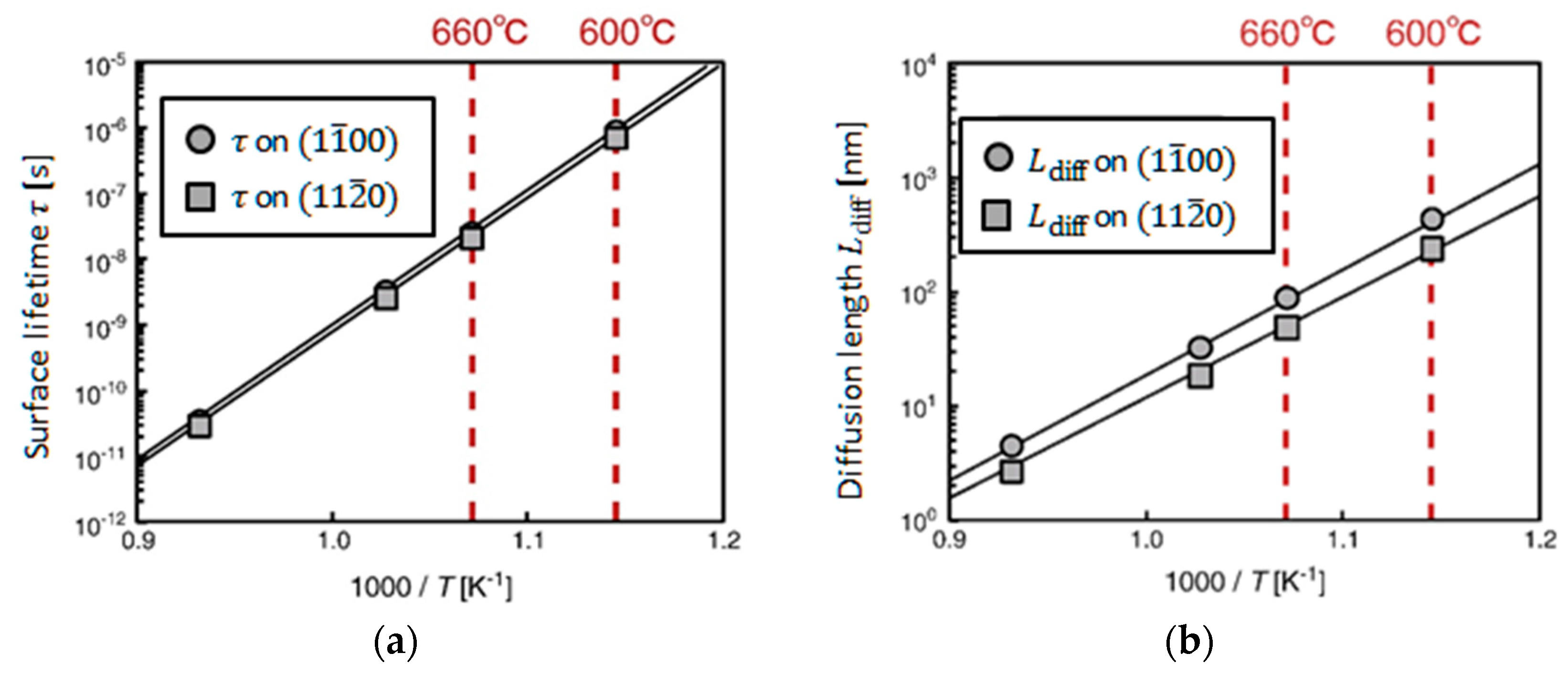
| Surface Orientation | τ (×10−7 s) | Ldiff (×102 nm) | Migration Barrier (eV) |
|---|---|---|---|
| (111)A | 22.4 | 16.3 | 0.13 |
| 8.57 | 4.36 | 0.27 | |
| 6.97 | 2.38 | 0.32 |
© 2017 by the authors. Licensee MDPI, Basel, Switzerland. This article is an open access article distributed under the terms and conditions of the Creative Commons Attribution (CC BY) license ( http://creativecommons.org/licenses/by/4.0/).
Share and Cite
Ito, T.; Akiyama, T. Recent Progress in Computational Materials Science for Semiconductor Epitaxial Growth. Crystals 2017, 7, 46. https://doi.org/10.3390/cryst7020046
Ito T, Akiyama T. Recent Progress in Computational Materials Science for Semiconductor Epitaxial Growth. Crystals. 2017; 7(2):46. https://doi.org/10.3390/cryst7020046
Chicago/Turabian StyleIto, Tomonori, and Toru Akiyama. 2017. "Recent Progress in Computational Materials Science for Semiconductor Epitaxial Growth" Crystals 7, no. 2: 46. https://doi.org/10.3390/cryst7020046