
On the Role of AlN Insertion Layer in Stress Control of GaN on 150-mm Si (111) Substrate
by

Po-Jung Lin
1,2, 
Ching-Ho Tien
1,
Tzu-Yu Wang
1,
Che-Lin Chen
2,
Sin-Liang Ou
3,
Bu-Chin Chung
2 and
Dong-Sing Wuu
1,* 1
Department of Materials Science and Engineering, National Chung Hsing University, Taichung 40227, Taiwan
2
Hermes-Epitek Corporation, Hisinchu 30077, Taiwan
3
Department of Materials Science and Engineering, Da-Yeh University, Changhua 51591, Taiwan
*
Author to whom correspondence should be addressed.
Crystals 2017, 7(5), 134; https://doi.org/10.3390/cryst7050134
Submission received: 12 April 2017
/
Revised: 5 May 2017
/
Accepted: 9 May 2017
/
Published: 12 May 2017
(This article belongs to the Special Issue Advances in GaN Crystals and Their Applications)
Abstract
:In this study, low-temperature (LT) and high-temperature (HT) AlN insertion layers (ILs) grown at 680 and 970 °C were integrated with 3.7-μm GaN-based heterostructure grown on 150-mm Si (111) substrates by metalorganic chemical vapor deposition. Under a V/III flow ratio of 1960, the GaN epilayer with a continuous interface resulting from the LT AlN IL was subject to a compressive stress of −0.109 GPa. However, the GaN epilayer with discontinuous interfaces resulting from the HT AlN IL growth under the same flow ratio was subject to a tensile stress of 0.174 GPa. To realize continuous interfaces between the GaN epilayer and HT AlN IL, a higher V/III ratio of 5960 was utilized to suppress the decomposition of GaN. It results in changing the stress state of the GaN-based heterostructure from tensile to compressive. This strategic finding indicates that a stress-controllable GaN on Si can be achieved via the incorporation of HT AlN ILs. A minimum curvature at 5 km−1 is demonstrated for the 3.7-μm GaN-based heterostructure on a 150-mm Si (111) substrate, which has high potential for power switching device applications.
1. Introduction
High-frequency and high-power electronic devices implemented by GaN on Si (111) technology have been realized in recent years. Low-cost and large-diameter wafers are major advantages of Si substrates. AlGaN/GaN high-electron-mobility transistors have been characterized by the high breakdown field and low on-resistance, which exhibit a 100-fold higher figure of merit (VB2/Ron) over Si-powered devices. The GaN-based materials are expected to improve power conversion efficiency and contribute to module miniaturization [1]. However, the dislocations and surface cracks caused by the −16.94% mismatch of the in-plane lattice constants and the 55% mismatch of the thermal expansion coefficients (TECs) pose limitations to growing high-quality, thick, crack-free GaN epilayers on Si substrates. Because the in-plane lattice constant of AlN (a0 = 3.11 Å) is lower than that of GaN (a0 = 3.18 Å), a GaN epilayer grown on an AlN intermediate layer will induce the compressive stress that compensates the tensile stress induced by the TEC mismatch between GaN and Si during the cooling process. Therefore, investigating the AlN insertion layers for stress engineering in the growth of GaN-on-Si heterostructure is imperative.
Researchers have been attempting to realize high-breakdown-voltage GaN-based devices by using an AlGaN transition layer, Al(Ga)N/GaN strained-layer superlattices [2,3,4] and AlN insertion layers (ILs) [5,6]. Ubukata et al. [7] used a strained-layer superlattice with 4-nm AlN layers and 20-nm GaN layers to maintain compression without relaxation for controlling the strain. The ratio of AlN/GaN layers in the strained-layer superlattice has also been investigated to control the stress [8]. Dadgar et al. [9,10] reported a mechanism for inducing stress by inserting the low-temperature (LT) and high-temperature (HT) AlN ILs into the GaN epilayers. The relaxed LT AlN ILs will induce the compressive stress to the subsequent GaN epilayer, which is essential for tension compensation during the wafer cooling. Compared with the result of LT AlN ILs insertion, strained HT AlN ILs induced less compressive stress in the subsequent GaN layer growth and thus lost the ability to overcome the tension.
On the other hand, the cracks or voids also play an important role in the stress control of GaN on Si (111) substrates. Bethoux et al. [11] achieved high-quality AlGaN epilayers grown laterally with suitable apertures between the crack edges. Tang et al. [12] indicated that buried cracks caused by AlN ILs could mitigate the thermal mismatch strain between GaN and Si. Ravikiran et al. [13] has demonstrated that raising the density of buried cracks reduces the residual compressive stress in the GaN epilayer, which can be attributed to the increased relaxation resulting from the cracks. These researchers have discovered that these buried cracks were generated after inserting the AlN ILs. When an AlN interlayer is grown on the GaN at high temperatures, the tension caused by the in-plane lattice mismatch between AlN and GaN induces cracks in the AlN, and results in creating apertures on the surface of the GaN epilayer. At such a high growth temperature (i.e., 920 °C), the Ga out-diffusion and decomposition of the GaN epilayer occur along the GaN [110] crystalline directions, which gives rise to buried cracks or voids after the subsequent epilayer growth. These buried cracks and voids can reduce the compressive stress which compensates the tensile stress during the cooling process after growth.
In this study, the stress behavior induced by inserting the LT and HT AlN ILs into the GaN epilayers was investigated. Controlling the generation of buried voids during the growth of HT AlN ILs is also discussed. Because ammonia (NH3) acts as the nitrogen source in the GaN growth, the generation of buried voids can be varied by the NH3 flow rate (i.e., V/III ratio) during changes in the growth condition from GaN to AlN IL at high temperature. A stress-controllable GaN-based heterostructure (3.7 μm thick) on 150 mm Si (111) with HT AlN ILs will be reported.
2. Results and Discussion
2.1. Epitaxial Structures
Four kinds of GaN-based heterostructures with the same total thickness of 3.7 μm were grown on 150-mm Si (111) substrates using metalorganic chemical vapor deposition (MOCVD). The growth sequences for the epi-structures of these structures A, B, and C shown in Figure 1a are described as follows: a 150-nm AlN buffer layer was grown on the Si (111) substrate to avoid the melt back caused by the reaction between Ga and Si. Subsequently, a 250-nm AlxGa1-xN transition layer (x = 0.25) was inserted between the AlN buffer layer and a 420-nm GaN epilayer to reduce the lattice mismatch between AlN and GaN. Four pairs of a 20-nm AlN IL and a subsequent 700-nm GaN epilayer were grown on top of the 420-nm GaN epilayer to control the stress. Table 1 shows NH3 flow rates, V/III ratio and the growth temperatures of structures A, B, and C. Under a NH3 flow rate of 4 slm (V/III ratio = 1906), LT and HT AlN ILs were grown in structures A and B at 680 and 970 °C, respectively. Compared with structure B, structure C was grown with HT AlN ILs under an NH3 flow rate of 12.5 slm (V/III ratio = 5956). The growth temperatures of AlN buffer layers, AlGaN transition layers, and GaN epilayers were 1085, 1060, and 1050 °C, respectively. Whereas, the corresponding NH3 flow rates for growing these layers were 4, 15, and 30 slm, respectively. The pressures of the epilayers prepared with and without the Al element were 50 mbar and 200 mbar, respectively. Because the pre-reaction between NH3 and trimethylaluminum was prevented at 50 mbar, the better crystalline quality of the epilayers with Al element could be realized. The GaN epilayers grown at 1050 °C required 400 and 120 s (at a rate of 1 °C/s) to cool to the temperatures of the LT and HT AlN ILs, respectively. In order to minimize the wafer curvature after cooling, the structure D was designed as shown in Figure 1b, which is nearly the same as the structure C except the top GaN stack layer. As displayed in Table 2, only one pair of a 20-nm AlN IL and a subsequent 2100-nm GaN epilayer was grown on top of the 1180-nm GaN epilayer to control the stress.
2.2. Epilayer Characteristics
Figure 2a depicts the bright-field scanning transmission electron microscopy (BF-STEM) cross-sectional image of structure A containing LT AlN ILs. The Si substrate, 150-nm AlN buffer layer, 250-nm AlGaN transition layer, 420-nm GaN epilayer, 20-nm LT AlN ILs, and 700-nm GaN epilayers are discernible in the figure. Dislocations of 420 nm-GaN generated by the lattice mismatch (19%) between AlN (a0 = 3.11 Å) and Si (111) (a0 = 5.43 Å) were suppressed after first 700-nm GaN grown on LT AlN IL by inducing the compressive stress [14,15]. As shown in Figure 2a, the dislocation density of 420 nm-GaN, first 700 nm-GaN, second 700 nm-GaN, third 700 nm-GaN, and fourth 700 nm-GaN were 1.3 × 10⁹, 6.2 × 10⁸, 6.2 × 10⁸, 5.5 × 10⁸, and 5.5 × 108 cm−2, respectively. This result indicates that the dislocation density of first 700 nm-GaN grown on LT AlN IL was suppressed than the density of 420 nm-GaN underlayer. After the first 700 nm-GaN, the GaN layers reveal a similar dislocation density. In Figure 2b, the distribution of the Si, Al, and Ga elements measured by energy-dispersive X-ray (EDX) are represented by various colors for sequentially distinguishing among the Si substrate, the AlN buffer layer, the AlGaN transition layer, the GaN epilayers, and the LT AlN ILs. As shown in Figure 2c,d, high angle-annular dark field (HAADF) and EDX measurements indicated that the interfaces between the LT AlN IL and the GaN epilayer are abrupt and that the Al element is limited completely in the LT AlN IL. The dark area in the grayscale image of Figure 2c represents a low atomic number for Al, whereas the bright area represents a high atomic number for Ga [16]; the thickness of the LT AlN ILs was 20-nm.
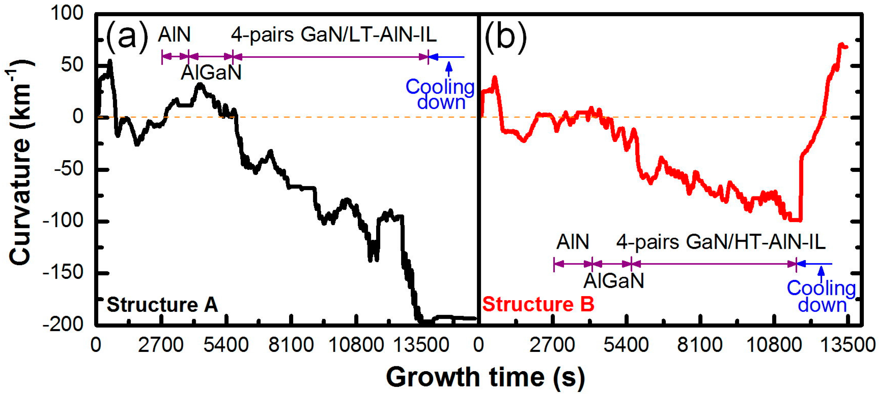
In situ curvature and temperature monitors were employed to characterize the stress and the temperatures of the structures during growth, and the results are illustrated in Figure 3. The AlN ILs of structures A and B were grown under 4 slm of NH3. Figure 3a shows the result of structure A with the LT AlN ILs grown at 680 °C. During the growth of the GaN epilayers, the curvature dropped gradually to −200 km−1 when the LT AlN ILs were inserted. Due to the 55% mismatch of TECs between GaN and Si, the curvature should typically change from a negative (compression) to a positive (tension) value during wafer cooling process. However, the curvature maintained at −200 km−1 indicates that the Si substrate was subject to a plastic deformation during the growth of the GaN epilayers with the LT AlN ILs. This implies that the stress in the GaN epilayer was under a state of compression and that no cracks appeared on the surface. Whereas, Figure 3b illustrates the result of structure B with the HT AlN ILs grown at 970 °C during the growth of the GaN epilayers, the curvature of structure B gradually dropped to −100 km−1 when the HT AlN ILs were inserted. Then, during cooling process, the curvature changed considerably to 75 km−1, indicating the generation of tension and cracks on the surface. This is a typical result of growing a GaN epilayer on a Si substrate. The results of the GaN epilayers containing the LT and HT AlN ILs, as shown in Figure 3, indicated general variations of stress in the GaN epilayers.
Room-temperature Raman spectra were used to quantify the stress of the GaN epilayers through a Raman shift of an E2 (high) peak. The A1 (LO) and E2 (high) modes of GaN are shown in Figure 4a [17,18]. The frequency of the E2 (high) phonon peak of unstressed GaN is 567.6 cm−1, which is generally used to evaluate the strain in epilayers [18]. The stress of the epilayers was calculated according to the Raman shift by solving for σxx = Δω/K, where Δω is the difference in the E2 (high) phonon peaks between the stressed and unstressed GaN epilayers, and K (−4.3 cm−1 GPa−1) is the strain coefficient [19,20].
As shown in Figure 4b, the positions of the E2 (high) peak measured from structures A and B were 568.07 and 566.85 cm−1, respectively. The E2 (high) peak in structure A shifted to a high frequency compared with that of unstressed GaN, indicating that the GaN epilayer was under a compressive stress of −0.109 GPa. By contrast, the E2 (high) peak in structure B shifted to a low frequency compared with that of unstressed GaN, indicating that the GaN epilayer was under a tensile stress of 0.174 GPa. After cooling, the GaN epilayers containing the LT and HT AlN ILs were both subject to a compressive stress and a tensile stress, respectively. The results shown in Figure 3 and Figure 4 are consistent with those reported by Dadgar et al., who demonstrated that the strain relaxation of GaN epilayers by inserting LT AlN ILs can further accumulate the compressive stress during the growth of GaN on Si [9,10]. Therefore, the relaxed LT AlN ILs can induce compressive stress to the subsequent GaN epilayer, whereas strained HT AlN ILs cannot induce sufficient compressive stress to the subsequent GaN epilayer. In our case, we demonstrate the effect of the GaN/AlN IL/GaN interfaces on the stresses of the GaN epitaxial structure grown on a Si substrate. Meanwhile, the continuous interface of AlN IL could induce compression in the GaN epilayer. As compared to the continuous interface, the discontinuous interface of AlN IL could reduce the compression in the GaN epilayer. To control the stress during growth, the growth temperature of AlN ILs is an effective factor for realizing a thick and crack-free GaN epilayer on a Si substrate.
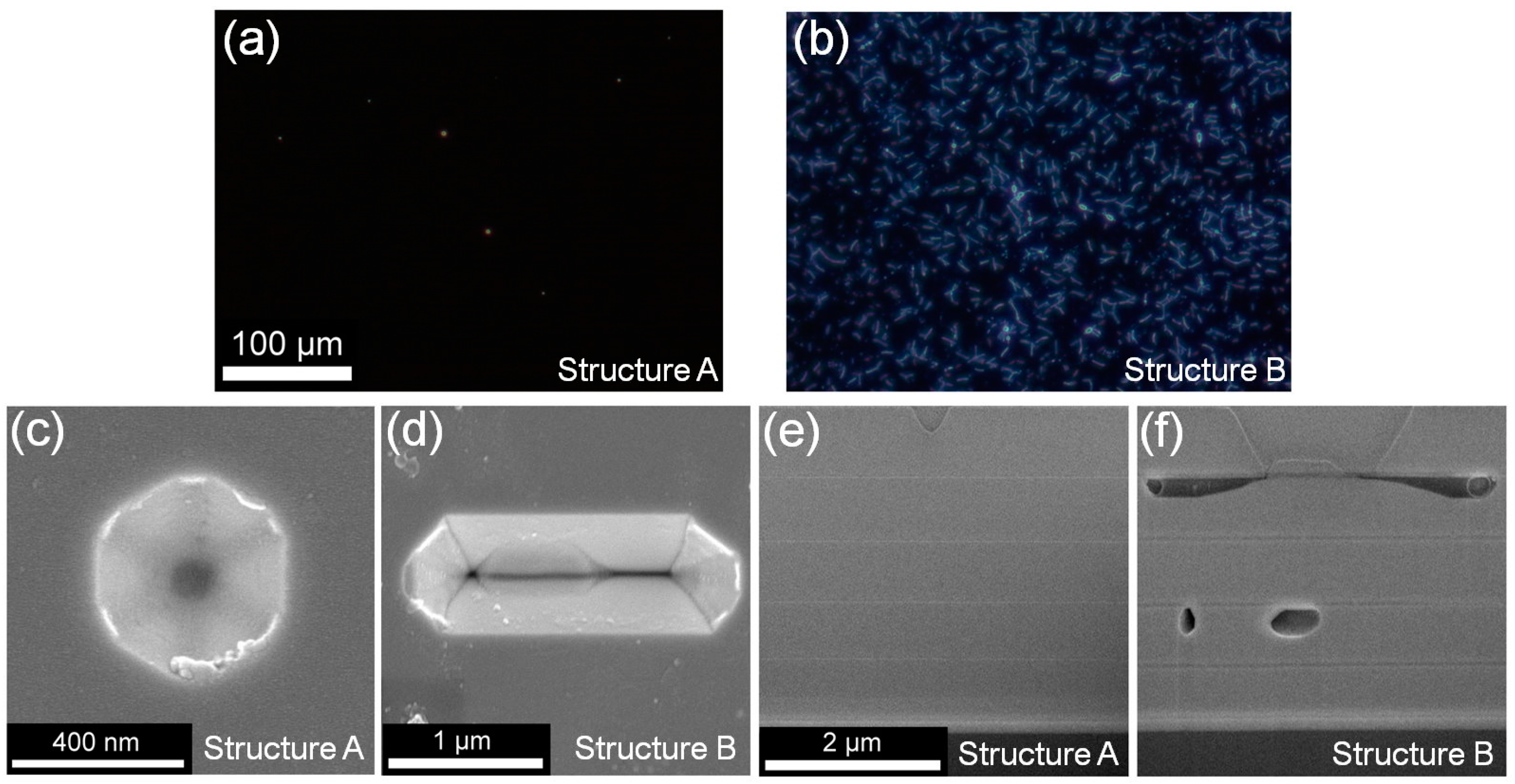
Figure 5a,b depict the dark-field optical microscopy (OM) images used to characterize the surface of structures A and B. As shown in Figure 5a, only a few epitaxial pits were present on the surface of structure A (LT AlN ILs). The pits could originate from the rough interface caused by the LT AlN ILs. Compared with the pits of structure A, two types of defects—namely strip defects (cracks or voids) and pits—were observed for structure B containing HT AlN ILs, as shown in Figure 5b. To inspect all the defects shown in Figure 5b, the focal length was adjusted to be below the surface of structure B. This is to confirm that certain defects in structure B were buried in the epilayer.
Figure 5c,d illustrate the surface of structures A and B, respectively, by focus-ion-beam scanning electron microscopy (FIB-SEM). The epitaxial pits have a hexagonal shape which is caused by screw dislocations propagating to the surface. However, the origin of the strip pits shown in Figure 5d is more complicated. FIB-SEM was employed to inspect the generation of the pits under the surfaces by examining the cross-sectional images shown in Figure 5e,f. The cross-sectional image depicting the area below the pit (Figure 5c,e) indicates the presence of a pit and the interfaces between the GaN epilayers and LT AlN ILs are continuous. A continuous interface can induce compression during the growth of the subsequent GaN epilayer, and this compressive stress is proportional to the number of AlN ILs. This is the reason the Si substrate and the GaN epilayer in structure A underwent a plastic deformation and compression. However, in structure B, the cross-sectional image depicting the area below the strip pit (Figure 5d,f) indicates that, in addition to the strip pits on the surface, voids are present between the interfaces of the 700-nm GaN epilayers and HT AlN ILs. Due to this, the interfaces are discontinuous. The generation of voids was caused by the apertures of cracked AlN ILs grown at temperatures higher than 900 °C [11,12] and insufficient NH3 flow rate (4 slm), which give rise to Ga diffusion and GaN decomposition. In addition to the generation of voids caused by the cracked AlN ILs, etching of GaN is also another possible mechanism. During the transition of growth conditions from the 700-nm GaN epilayer to the HT AlN IL, the growth temperature was changed from 1050 to 970 °C and meantime the corresponding NH3 flow rate was changed from 30 to 4 slm. In this process, the temperature was higher than 970 °C and the NH3 flow could be insufficient to prevent the GaN from decomposition. The surface of the GaN epilayer was exposed to the ambience of decomposition, which caused the etched voids along the GaN <> crystalline directions. From the bottom to the surface of the GaN epilayer grown on Si, voids were generated separately from the interface and extended into to a large strip pit, and finally, discontinuous interfaces and a large pit were observed for the GaN epilayer prepared on Si. The discontinuous interface induced less compressive stress to the subsequent GaN epilayer. In the cooling process, compressive stress accumulated during GaN growth is used to compensate the tensile stress caused by the TEC mismatch between GaN and Si. Therefore, structure B with discontinuous interfaces and less compressive stress, resulted in tensile stress after the wafer cooling process. Note that a sufficient NH3 flow plays a critical role to prevent the decomposition of GaN at high temperature. To quantitatively study the crystalline quality, the GaN epilayers of structures A and B were examined by X-ray diffraction (XRD). The rocking curves of GaN (0002) and () for structures A and B are shown in Figure 6. In contrast to structure A with the full width at half-maximum (FWHM) values of GaN (0002) for 483 arcsec and GaN () for 1098 arcsec, structure B with discontinuous interfaces and large pits has the higher FWHM values in GaN (0002) and () for 750 and 1251 arcsec, respectively. The FWHM of ω-scan and mosaic model can be described as [21]
where βω is the FWHM measured from different reflections; and are the contributions of screw and edge dislocations to the FWHM of ω-scan. ρe and ρs are the edge and screw dislocation densities; Δωs and Δωe are referred to as tilt and twist, which can be calculated by FWHM of (0002) and , respectively. and are the Burgers vectors of edge-type and screw-type dislocations, respectively. We have estimated the dislocation density from the FWHM of GaN (0002) and (). The densities of the screw and edge dislocations of structure A were 2.27 × 10⁸ and 3.05 × 109 cm−2, and structure B for 5.46 × 10⁸ and 3.91 × 109 cm−2, respectively. The results indicate that structure A grown with LT AlN ILs shows higher crystalline quality than structure B.
Other than the NH3 flow rate, structures B and C were grown under the same growth conditions. The structures were used to examine the effect of changing NH3 flow rate from 4 to 12.5 slm for stress control. The in situ curvature of structures B and C are illustrated in Figure 7. During the growth of the GaN epilayers, the curvatures of structures B and C with HT AlN ILs prepared at NH3 flow rates of 4 and 12.5 slm, dropped to −75 and −225 km−1, respectively. After cooling, the Si substrate and the GaN epilayer in structure C underwent a plastic deformation and compression, indicating that the adjustment of the NH3 flow rate from 4 to 12.5 slm leads to the stress changed from a state of tension to compression. The cross-sectional image shown in Figure 7 indicates that most of the interfaces between the GaN epilayers and HT AlN ILs are continuous, confirming that adjusting the NH3 flow rate can suppress GaN decomposition to realize a continuous interface and a stress-controllable GaN epilayer on Si with HT AlN ILs.
Figure 8 illustrates stages A–E, to represent the sequence of discontinuous interface and strip pit generation during HT-AlN IL growth under insufficient NH3 flow. In stage A, a 420-nm GaN epilayer is grown on top of the epi structure, which consists of the AlN buffer layer and the AlGaN transition layer. During stage B, the NH3 flow and temperature changes gradually from 30 to 4 slm and from 1050 °C to 970 °C, respectively; here, the temperature is higher than 970 °C and the NH3 flow could be insufficient to prevent the GaN from decomposing. Furthermore, the surface of the GaN epilayer is exposed to the ambience of decomposition, which produces etched voids. Combined with the decreasing NH3 flow, a strip void emerges along the GaN [110] crystalline directions in stage C. In stage D, the HT AlN IL is grown on the etched GaN epilayer, however, this growth is discontinuous because of the strip void generation. Finally, in stage E, a 700-nm GaN epilayer is grown on the HT AlN IL. However, the strip void caused by GaN decomposition is too large to be flattened laterally; thus, a strip pit is produced on the surface of the 700-nm GaN epilayer.
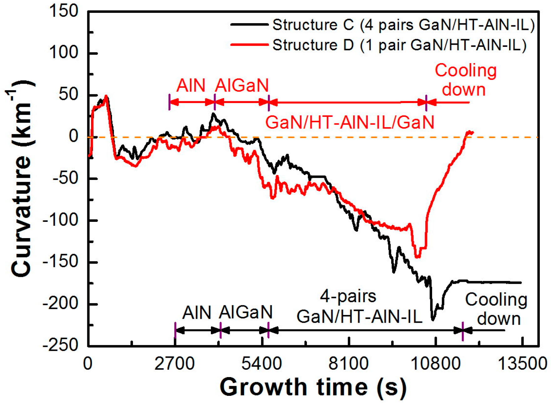
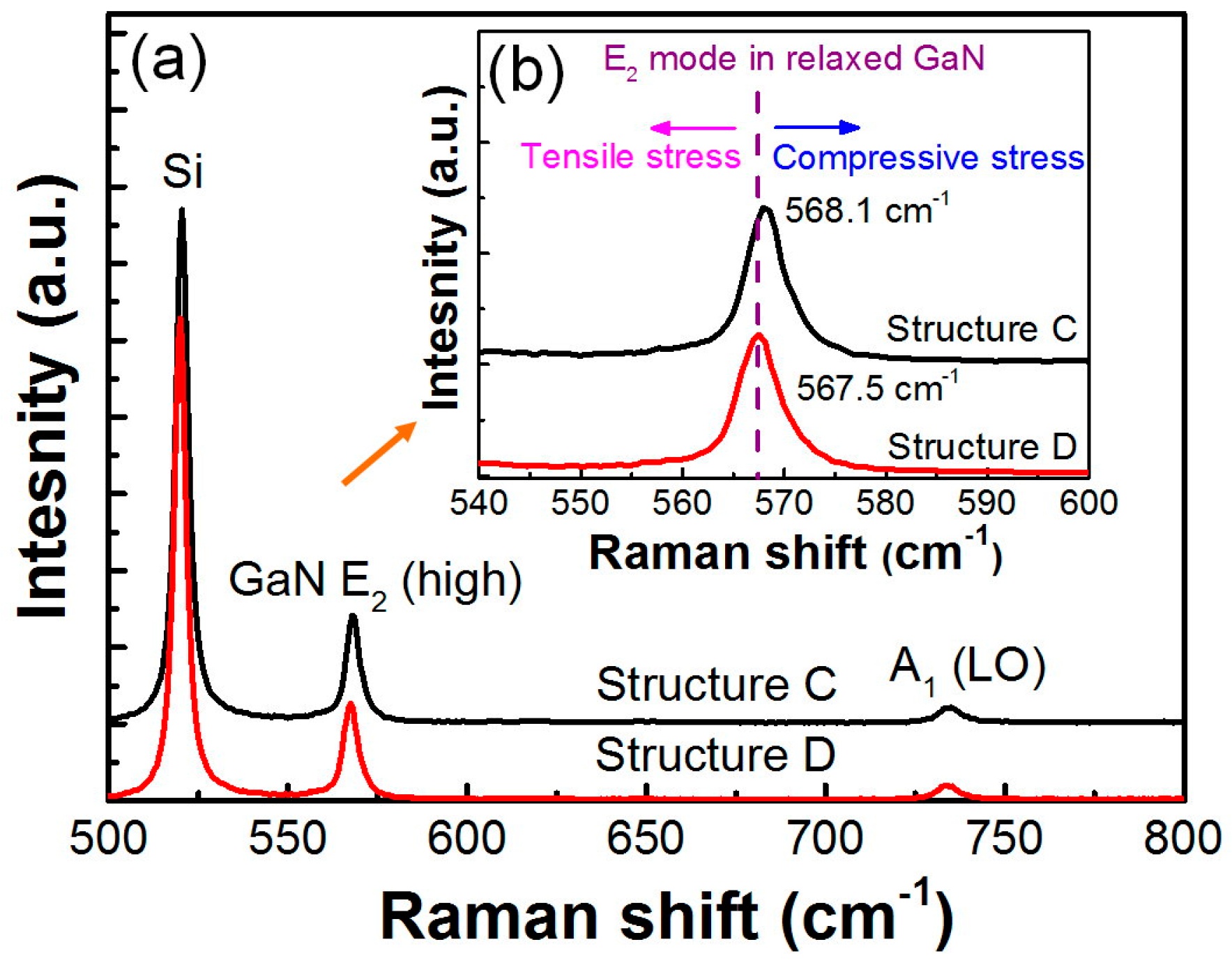
The voids generated between the interfaces of the 700-nm GaN epilayers and HT AlN ILs are explained by the results of structure B and C. During the transition of growth conditions from the 700-nm GaN epilayer to the HT AlN IL, providing sufficient NH3 flow can suppress the decomposition of the 700-nm GaN epilayer to realize continuous interfaces and stress-controllable GaN epilayers. Because the compressive stress of structure C was high during the GaN epilayer growth, the Si substrate was subject to plastic deformation. Therefore, the curvature of structure C was maintained at −225 km−1 after cooling. An ideal wafer curvature should approximate 0 km−1 after cooling, which means that the bow in the wafer is flatter and more suitable for devices process. To improve the curvature of structure C (Figure 7), the stress caused by the GaN epilayer should be controllable during growth by adjusting the number of continuous interfaces between the 700-nm GaN epilayer and HT AlN IL. Therefore, the adjusted structure D with one HT AlN IL is shown in Figure 1b; the total thickness of the GaN epilayer remains 3.7 μm. The growth parameters for structure D are same as for structure C. Moreover, the GaN epilayers directly below and above the HT AlN are 1180 and 2100 nm, respectively. The growth parameters of structure D are the same as for structure C. Figure 9 indicates that the curvature of structure D, which has one HT AlN IL, approximates 5 km−1 after cooling. As shown in Figure 10, the positions of the E2 (high) peak for structures C and D were 568.1 and 567.5 cm−1, respectively. The E2 (high) peak of structure C shifted to higher frequency side than that of unstressed GaN, indicating a compressive stress of −0.116 GPa. For structure D, the E2 (high) peak shifted to lower frequency side indicates a tensile stress of 0.023 GPa. Because there is one HT AlN IL and several continuous interfaces between the GaN epilayers and HT AlN IL, the generated compressive stress during the growth of the GaN epilayers was moderate and the Si substrate of structure D was not subjected to plastic deformation. The results in Figure 9 and Figure 10 show that adjusting the number of continuous interfaces affects the GaN epilayer stress, and the wafer bow of structure D is flatter than that of structure C after cooling.
3. Materials and Methods
The 3.7-μm GaN-based heterostructures used in this work were grown on 150-mm Si (111) substrates by using a MOCVD system produced by Hermes-Epitek Corp. Trimethylgallium, trimethylaluminum, and NH3 were the source materials for gallium, aluminum, and nitrogen, respectively. Hydrogen was used as the carrier gas for the growth process. Surface and cross-sectional images of the 3.7-μm epilayers were characterized through dark-field OM, FIB-SEM, and BF-STEM. The HAADF imaging and EDX spectroscopy were also performed to characterize the distribution of the compositions of the GaN epilayers prepared with the AlN ILs. An in situ curvature monitor and a room-temperature Raman scattering spectroscopy were used to investigate the stress characteristics of the grown epilayers. Room-temperature Raman scattering spectroscopy (LABRAM HR 800 UV, Horiba/Jobin-Yvon, Longjumeau, France) was utilized to study the stress of epilayers with excitation source of 488-nm. An XRD (X’Pert PRO MRD, PANalytical, Holland) measurement was used to determine the FWHM of the rocking curve for GaN with structures A and B.
4. Conclusions
In conclusion, 3.7-μm GaN epilayers with 20-nm LT (680 °C) and HT (970 °C) AlN ILs were grown on 150-mm Si (111) substrates. After growth, structures A (with LT AlN ILs) and B (with HT AlN ILs) were subject to a compressive stress of −0.109 GPa and tensile stress of 0.174 GPa, respectively. The stress, depending on the growth temperature of the AlN ILs, was caused by the conditions of the interface between the GaN epilayers and AlN ILs. During the growth of HT AlN ILs with insufficient NH3 flow rate of 4 slm, voids were generated easily through the decomposition of GaN. The voids led to discontinuous interfaces and extended into a large strip pit on the surface. A sufficient NH3 flow rate of 12.5 slm was used to suppress void generation and the decomposition of GaN during the growth of HT AlN ILs, and resulted in a highly continuous interface between the GaN epilayers and HT AlN ILs. The continuous interface could induce compression in the GaN epilayer, and the discontinuous interface induced less compression in the GaN epilayer. On basis of the results, a stress-controllable GaN epilayer was demonstrated by adjusting the number of HT AlN IL.
Acknowledgments
This work was supported by the Ministry of Science and Technology (Taiwan, R.O.C.) under Grant numbers 104-2221-E-005-036-MY3 and 105-2622-8-005-003-TE1. We would like to thank Chih-Sheng Wu of Hermes-Epitek Corporation for his valuable discussion for the MOCVD growth and system maintenance.
Author Contributions
Po-Jung Lin, Che-Lin Chen, and Bu-Chin Chung conceived and designed the experiments. Po-Jung Lin, Che-Lin Chen, Tzu-Yu Wang, and Sin-Liang Ou contributed the film measurements. Ching-Ho Tien, Tzu-Yu Wang, and Dong-Sing Wuu analyzed and verified the data. Po-Jung Lin and Dong-Sing Wuu wrote the manuscript. All authors read and approved the final version of the manuscript to be submitted.
Conflicts of Interest
The authors declare no conflict of interest.
References
- Millán, J.; Godignon, P.; Perpiñà, X.; Pérez-Tomés, A.; Rebollo, J. A survey of wide band gap semiconductor devices. IEEE Trans. Power Electron. 2014, 29, 2155–2163. [Google Scholar] [CrossRef]
- Yano, Y.; Tokunaga, H.; Shimamur, H.; Yamaoka, Y.; Ubukata, A.; Tabuchi, T.; Matsumoto, K. Control of thickness and composition variation of AlGaN/GaN on 6-and 8-in substrates using multiwafer high-growth-rate organic chemical vapor deposition tool. Jpn. J. Appl. Phys. 2013, 52, 08JB06. [Google Scholar] [CrossRef]
- Selvaraj, S.L.; Watanabe, A.; Wakajima, A.; Egawa, T. 1.4-KV breakdown voltage for AlGaN/GaN high-electron-mobility transistors on silicon substrate. IEEE Electron Device Lett. 2012, 33, 1375–1377. [Google Scholar] [CrossRef]
- Feltin, E.; Beaumont, B.; Laügt, M.; Mierry, P.; Vennéguès, P.; Lahrèche, H.; Leroux, M.; Gibart, P. Stress control in GaN grown on silicon (111) by metalorganic vapor phase epitaxy. Appl. Phys. Lett. 2001, 79, 3230–3232. [Google Scholar] [CrossRef]
- Frayssinet, E.; Cordier, Y.; Schenk, H.P.D.; Bavard, A. Growth of thick GaN layers on 4-in. and 6-in. silicon (111) by metal-organic vapor phase epitaxy. Phys. Status Solidi C 2011, 8, 1479–1482. [Google Scholar] [CrossRef]
- Schenk, H.P.D.; Frayssinet, E.; Bavard, A.; Rondi, D.; Cordier, Y.; Kennard, M. Growth of thick, continuous GaN layers on 4-in. Si substrate by metalorganic chemical vapor deposition. J. Cryst. Growth 2011, 1, 85–91. [Google Scholar] [CrossRef]
- Ubukata, A.; Ikenaga, K.; Akutsu, N.; Yamaguchi, A.; Matsumoto, K.; Yamazaki, T.; Egawa, T. GaN growth on 150-mm-diameter (111) Si substrates. J. Cryst. Growth 2007, 298, 198–201. [Google Scholar] [CrossRef]
- Lin, P.R.; Huang, S.Y.; Wang, W.K.; Chen, L.; Chung, B.C.; Wuu, D.S. Controlling the stress of growing GaN on 150-mm Si (111) in an AlN/GaN strained layer superlattice. Appl. Surf. Sci. 2016, 362, 434–440. [Google Scholar] [CrossRef]
- Dadgar, A.; Bläsing, J.; Diez, A.; Alam, A.; Heulen, M.; Krost, A. Metalorganic chemical vapor phase epitaxy of crack-free GaN on Si (111) exceeding 1 μm in thickness. Jpn. J. Appl. Phys. 2000, 39, L1183. [Google Scholar] [CrossRef]
- Reiher, A.; Bläsing, J.; Dadgar, A.; Diez, A.; Krost, A. Efficient stress relief in GaN heteroepitaxy on Si(111) using low-temperature AlN interlayers. J. Cryst. Growth 2003, 248, 563–567. [Google Scholar] [CrossRef]
- Bethoux, J.M.; Vennéguès, P.; Natali, F.; Feltin, E.; Tottereau, O.; Nataf, G.; De Mierry, P.; Semond, F. Growth of high quality crack-free AlGaN films on GaN templates using plastic relaxation through buried cracks. J. Appl. Phys. 2003, 94, 6499–6507. [Google Scholar] [CrossRef]
- Tang, H.; Baribeau, J.M.; Aers, G.C.; Fraser, J.; Rolfe, S.; Bardwell, J.A. Role of buried cracks in mitigating strain in crack free GaN geown Si (111) employing AlN interlayer schemes. J. Cryst. Growth 2011, 323, 413–417. [Google Scholar] [CrossRef]
- Ravikiran, L.; Radhakrishnan, K.; Dharmarasu, N.; Agrawal, M.; Basha, S. Munawar Strain states of AlN/GaN mitigating layer and their effect on GaN buffer layer grown by ammonia molecular beam epitaxy on 100-mm Si (111). J. Appl. Phys. 2013, 114, 123503. [Google Scholar] [CrossRef]
- Romanov, A.E.; Speck, J.S. Stress relaxation in mismatched layers due to threading dislocation inclination. Appl. Phys. Lett. 2003, 83, 2569–2571. [Google Scholar] [CrossRef]
- Fritze, S.; Drechsel, P.; Stauss, P.; Rode, P.; Markurt, T.; Schulz, T.; Albrecht, M.; Bläsing, J.; Dadgar, A.; Krost, A. Role of low-temperature AlGaN interlayers in thick GaN on silicon by metalorganic vapor phase epitaxy. J. Appl. Phys. 2012, 111, 124505. [Google Scholar] [CrossRef]
- Walther, T.; Humphreys, C.J. A quantitative study of compositional profiles of chemical vapour-deposited strained silicon-germanium/silicon layers by transmission electron microscopy. J. Cryst. Growth. 1999, 197, 113–128. [Google Scholar] [CrossRef]
- Davydow, V.Y.; Goncharuk, I.N.; Smirmov, A.N.; Nikolaev, A.E.; Lundin, W.V.; Usikov, A.S.; Klochikhin, A.A.; Aderhold, J.; Graul, J.; Semchinova, O.; et al. Composition dependence of optical phonon energies and Raman line broadening in hexagonal AlxGaN1-xN alloys. Phys. Rev. B 2002, 65, 125203. [Google Scholar] [CrossRef]
- Davydow, V.Y.; Kitaev, Y.E.; Goncharuk, I.N.; Smirmov, A.N.; Graul, J.; Semchinova, O.; Uffmann, D.; Smirnov, M.B.; Mirgorodsky, A.P.; Evarestov, R.A. Phonon dispersion and Raman scattering in hexagonal GaN and AlN. Phys. Rev. B 1998, 58, 12899. [Google Scholar] [CrossRef]
- Wilson, A.F.; Wakejima, A.; Egawa, T. Influence of GaN stress on threshold voltage shift in AlGaN/GaN high-electron-mobility transistors on Si under off-state electrical bias. Appl. Phys. Express 2013, 6, 086504. [Google Scholar] [CrossRef]
- Tripathy, S.; Chua, S.J.; Chen, P.; Miao, Z.L. Micro-Raman investigation of strain in GaN and AlxGaN1-xN/GaN heterostructures grown on Si(111). J. Appl. Phys. 2002, 92, 3503–3510. [Google Scholar] [CrossRef]
- Liu, J.Q.; Wang, J.F.; Liu, Y.F.; Huang, K.; Hu, X.J.; Zhang, Y.M.; Xu, Y.; Xu, K.; Yang, H. High-resolution X-ray diffraction analysis on HVPE-grown thick GaN layers. J. Cryst. Growth 2009, 311, 3080–3084. [Google Scholar] [CrossRef]
Figure 1.
Scheme of (a) structures A, B, and C, and (b) structure D.
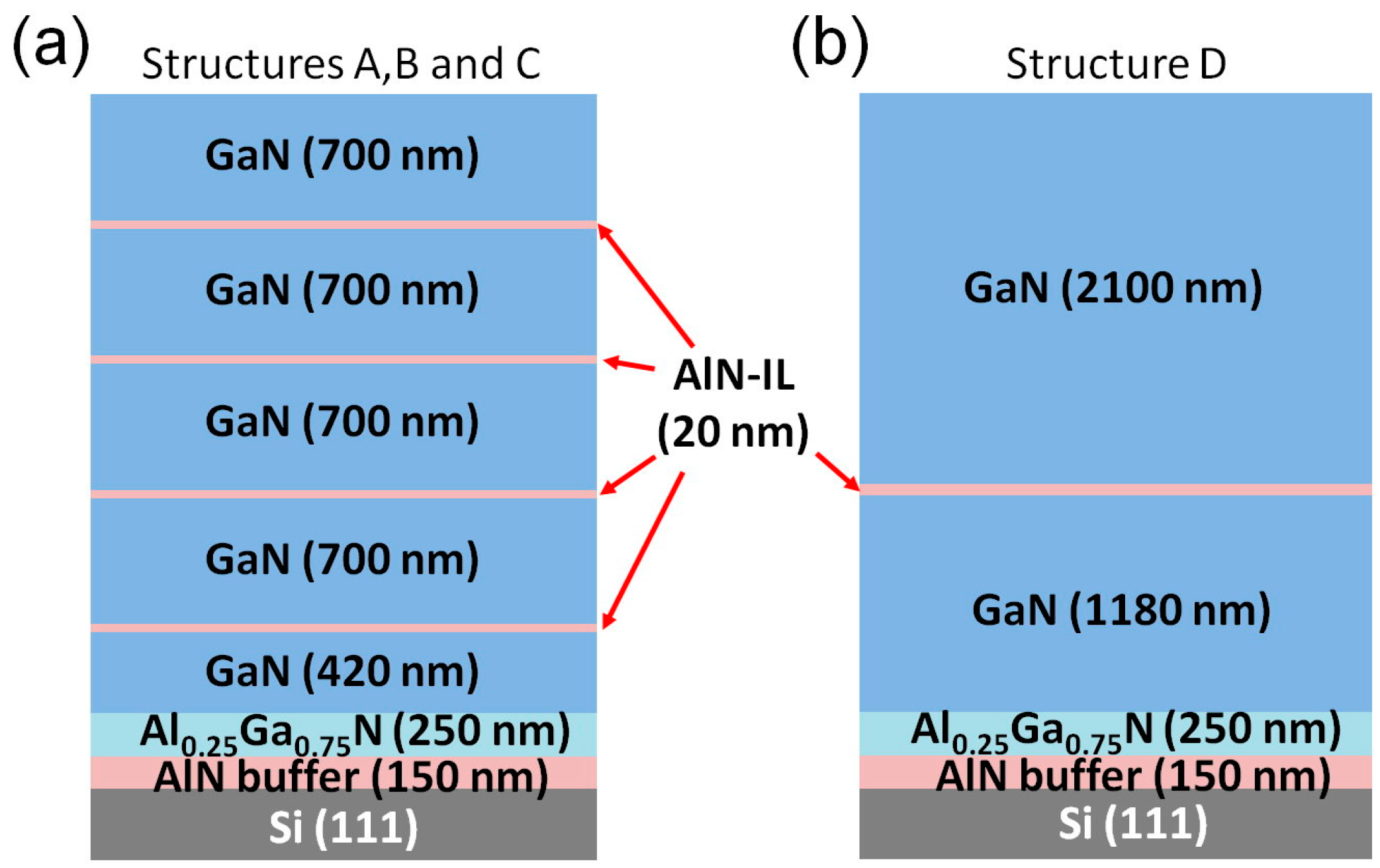
Figure 2.
(a) Cross-sectional BF-STEM image of structure A containing LT AlN ILs grown on the Si substrate; (b) distribution of Si, Al, and Ga measured with EDX; (c) HAADF image of an interface between GaN epilayers and an LT AlN IL; (d) distribution of Al and Ga of an interface between GaN epilayers and an LT AlN IL.
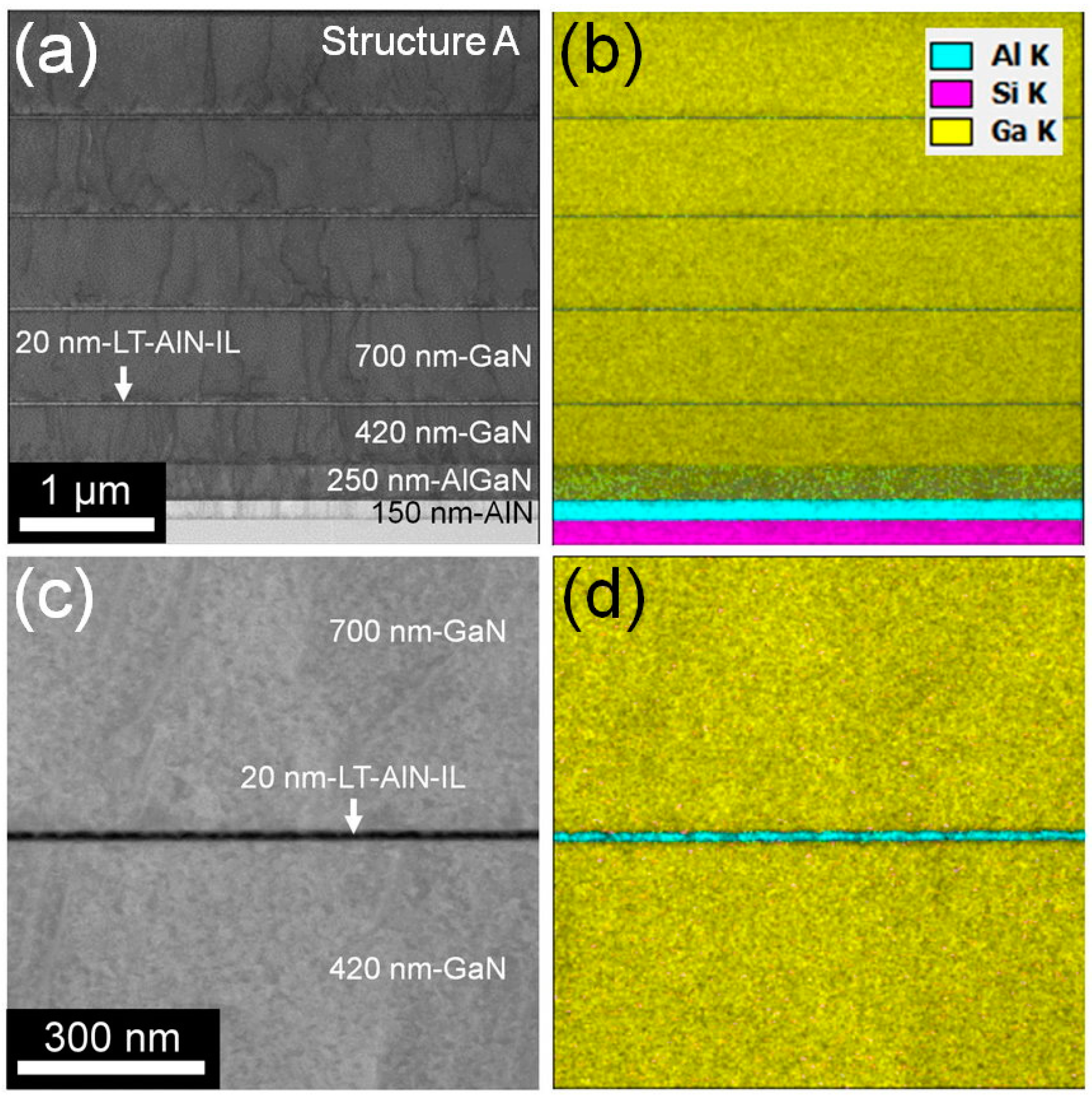
Figure 3.
(a) In situ curvature of structure A (black); (b) In situ curvature of structure B (red).

Figure 4.
(a) Raman spectra of structures A (black) and B (red) (b) Raman shift of E2 (high).
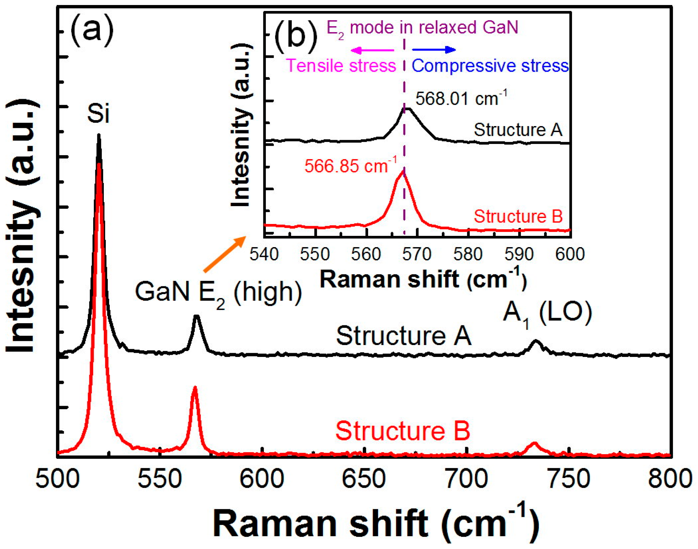
Figure 5.
(a) Dark-field OM image of structure A; (b) Dark-field OM image of structure B; (c) Plan-view image of a pit on the surface of structure A; (d) Plan-view image of a strip pit on the surface of structure B; (e) cross-sectional FIB-SEM image of structure A; (f) cross-sectional FIB-SEM image of structure B.

Figure 6.
(a) FWHM of GaN (0002) rocking curves of structures A and B; (b) FWHM of GaN () ricking curves of structures A and B.
Figure 6.
(a) FWHM of GaN (0002) rocking curves of structures A and B; (b) FWHM of GaN () ricking curves of structures A and B.
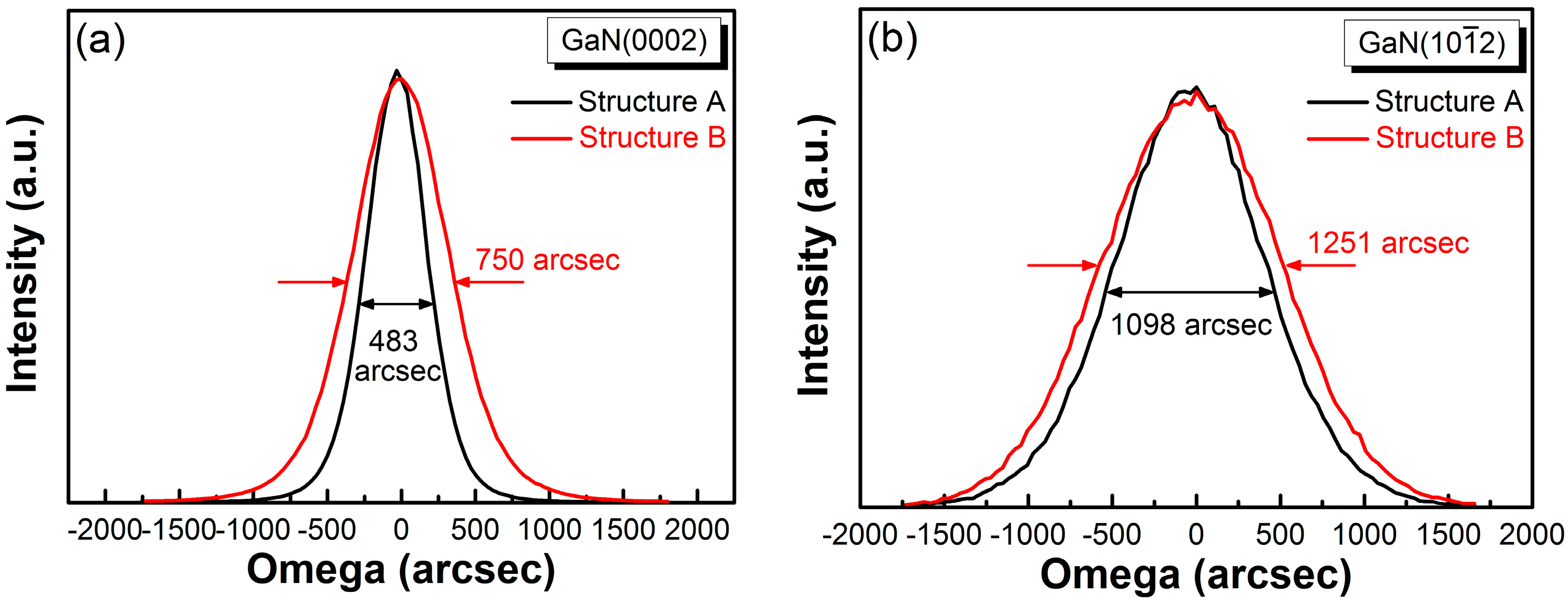
Figure 7.
In situ curvature of structures B (red) and C (Black); and cross-sectional FIB-SEM image of structure C.
Figure 7.
In situ curvature of structures B (red) and C (Black); and cross-sectional FIB-SEM image of structure C.

Figure 8.
Generation of strip pit with insufficient NH3.
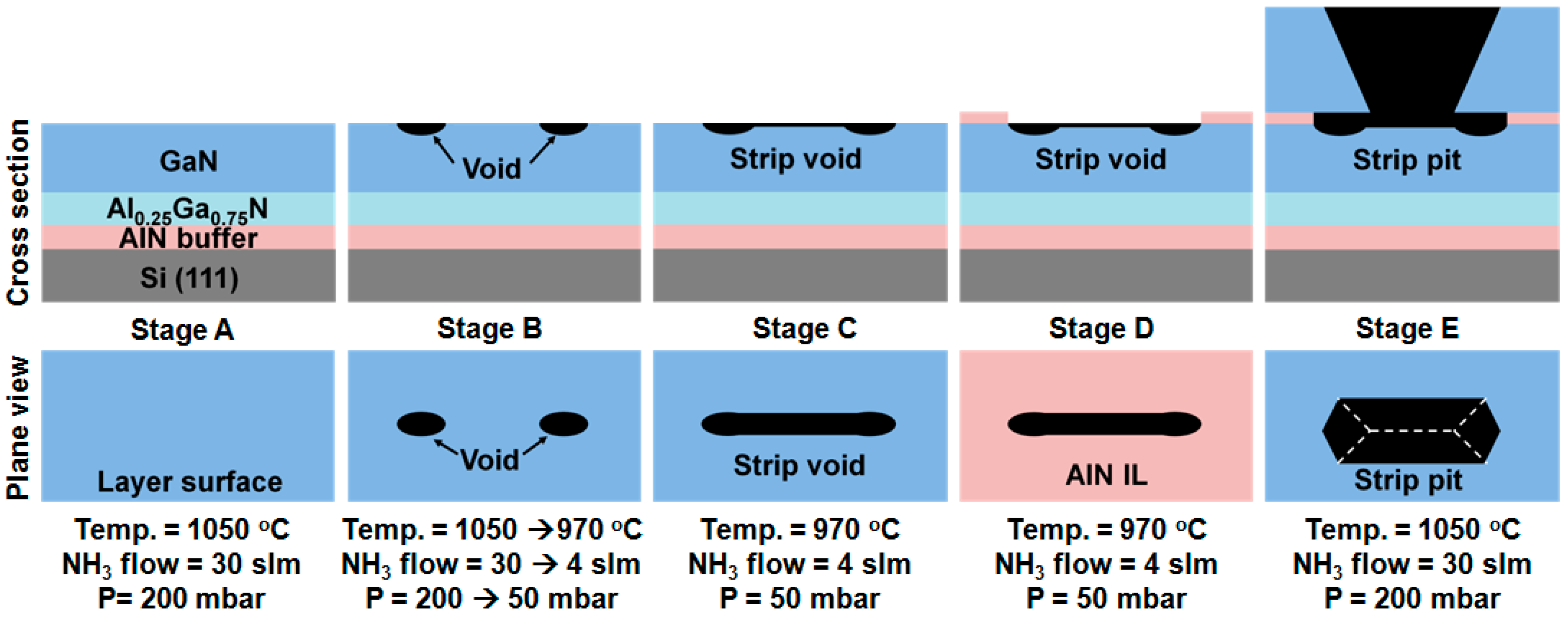
Figure 9.
In situ curvature of structures C (black) and D (red).

Figure 10.
(a) Raman spectra of structures C (black) and D (red) (b) Raman shift of E2 (high).


Table 1.
The growth parameters of structures A, B, and C.
| Growth Parameters | Structure A | Structure B | Structure C | |||||||
|---|---|---|---|---|---|---|---|---|---|---|
| Temp. (°C) | NH3 Flow (slm) | V/III Ratio | Temp. (°C) | NH3 Flow (slm) | V/III Ratio | Temp. (°C) | NH3 Flow (slm) | V/III Ratio | ||
| 4-pairs | GaN (700 nm) | 1050 | 30 | 1500 | 1050 | 30 | 1500 | 1050 | 30 | 1500 |
| AlN (20 nm) | 680 | 4 | 1906 | 970 | 4 | 1906 | 970 | 12.5 | 5956 | |
| GaN (420 nm) | 1050 | 30 | 1500 | 1050 | 30 | 1500 | 1050 | 30 | 1500 | |
| Al0.25Ga0.75N | 1060 | 15 | 3000 | 1060 | 15 | 3000 | 1060 | 15 | 3000 | |
| AlN buffer | 1085 | 4 | 1906 | 1085 | 4 | 1906 | 1085 | 4 | 1906 | |
Table 2.
The growth parameters of structure D.
| Growth Parameters | Structure D | |||
|---|---|---|---|---|
| Temp. (°C) | NH3 Flow (slm) | V/III Ratio | ||
| 1-pair | GaN (2100 nm) | 1050 | 30 | 1500 |
| AlN (20 nm) | 970 | 12.5 | 5956 | |
| GaN (1180 nm) | 1050 | 30 | 1500 | |
| Al0.25Ga0.75N | 1060 | 15 | 3000 | |
| AlN buffer | 1085 | 4 | 1906 | |
© 2017 by the authors. Licensee MDPI, Basel, Switzerland. This article is an open access article distributed under the terms and conditions of the Creative Commons Attribution (CC BY) license (http://creativecommons.org/licenses/by/4.0/).
Share and Cite
MDPI and ACS Style
Lin, P.-J.; Tien, C.-H.; Wang, T.-Y.; Chen, C.-L.; Ou, S.-L.; Chung, B.-C.; Wuu, D.-S. On the Role of AlN Insertion Layer in Stress Control of GaN on 150-mm Si (111) Substrate. Crystals 2017, 7, 134. https://doi.org/10.3390/cryst7050134
AMA Style
Lin P-J, Tien C-H, Wang T-Y, Chen C-L, Ou S-L, Chung B-C, Wuu D-S. On the Role of AlN Insertion Layer in Stress Control of GaN on 150-mm Si (111) Substrate. Crystals. 2017; 7(5):134. https://doi.org/10.3390/cryst7050134
Chicago/Turabian StyleLin, Po-Jung, Ching-Ho Tien, Tzu-Yu Wang, Che-Lin Chen, Sin-Liang Ou, Bu-Chin Chung, and Dong-Sing Wuu. 2017. "On the Role of AlN Insertion Layer in Stress Control of GaN on 150-mm Si (111) Substrate" Crystals 7, no. 5: 134. https://doi.org/10.3390/cryst7050134
Note that from the first issue of 2016, this journal uses article numbers instead of page numbers. See further details here.