Article

Structural and Electrical Properties Characterization of Sb1.52Bi0.48Te3.0 Melt-Spun Ribbons

1
Institut Jean Lamour, UMR 7198 CNRS, Université de Lorraine, Parc de Saurupt, CS 50840, 54011 Nancy, France
2
C2TN, Instituto Superior Técnico, Universidade de Lisboa, Estrada Nacional 10, 2695-066 Bobadela LRS, Portugal
*
Author to whom correspondence should be addressed.
Crystals 2017, 7(6), 172; https://doi.org/10.3390/cryst7060172
Submission received: 28 April 2017 / Revised: 1 June 2017 / Accepted: 7 June 2017 / Published: 13 June 2017
(This article belongs to the Special Issue Materials Processing and Crystal Growth for Thermoelectrics)

Abstract

:
Melt-spinning (MS) has been reported as a promising tool to tailor the microstructure of bulk thermoelectric materials leading to enhanced thermoelectric performances. Here, we report on a detailed characterization of p-type Bi0.48Sb1.52Te3 ribbons produced by melt-spinning. The microstructure of the melt-spun ribbons has been studied by means of X-ray diffraction, scanning and transmission electron microscopy (TEM). The analyses indicate that the ribbons are highly-textured with a very good chemical homogeneity. TEM reveals clear differences in the microstructure at large and short-range scales between the surface that was in contact with the copper wheel and the free surface. These analyses further evidence the absence of amorphous regions in the melt-spun ribbons and the precipitation of elemental Te at the grain boundaries. Low-temperature electrical resistivity and thermopower measurements (20–300 K) carried out on several randomly-selected ribbons confirm the excellent reproducibility of the MS process. However, the comparison of the transport properties of the ribbons with those of bulk polycrystalline samples of the same initial composition shows that MS leads to a more pronounced metallic character. This difference is likely tied to changes in deviations from stoichiometry due to the out-of-equilibrium conditions imposed by MS.

1. Introduction

Thermoelectric materials provide a versatile, environmentally-friendly way for generating electric power from waste heat or for Peltier cooling [1,2]. Despite the fact that this technology has been successfully used for decades to power deep-space probes and rovers, its applications remain limited to niche technologies for which the robustness of thermoelectric modules outweighs their low conversion efficiency [1,2]. A more widespread use of thermoelectric materials is therefore tied to the identification of novel families of materials exhibiting a high dimensionless thermoelectric figure of merit:
ZT = α2T/ρκ
where α is the thermopower, ρ is the electrical resistivity, κ is total the thermal conductivity and T is the absolute temperature; or to the optimization of the thermoelectric properties of state-of-the-art materials [1,2,3].
Most of the recently-discovered families of thermoelectric materials reach their maximum ZT values at high temperatures, typically between 700 and 1200 K [4,5,6,7,8,9,10,11,12]. For thermoelectric applications near room temperature, solid solutions of bismuth telluride Bi2Te3 with the isomorphous compounds Sb2Te3 and Bi2Se3 are still nowadays the best materials with ZT values around unity in both p- and n-type compounds [2]. The AV2BVI3 (A = Bi or Sb and B = Te or Se) compounds and their solid solutions crystallize in the R 3 ¯ m space group and are narrow-band-gap semiconductors with topologically-protected gapless surface states [2,13,14,15,16]. Their crystal structure is composed of repeated planes of five-atomic layer lamellas perpendicular to the trigonal axis separated by a van der Waals gap. This layered structure inevitably results in anisotropic transport properties in both single-crystalline and polycrystalline specimens [2].
Several synthesis techniques were used in the past to prepare these compounds either in single or bulk polycrystalline form [17,18,19,20,21,22,23,24,25]. Polycrystals are traditionally fabricated using the zone melting method, powder metallurgy techniques or mechanical alloying, followed by a consolidation step [26,27,28,29,30,31]. The melt-spinning (MS) method, based on rapid solidification of the melt that allows attaining cooling rates as high as 104–107 K s−1, has been used to produce these materials by Soviet Union and Russian research groups [32,33,34,35]. Starting from raw materials, MS produces ribbons, flakes or foils, which are in an out-of-equilibrium state due to the high quenching rate leading to particular microstructures and physical properties. This technique has also been the subject of studies from a mathematical point of view [36]. Recently, this technique combined with subsequent hot pressing was employed successfully by several groups to achieve high thermoelectric performance with peak ZT values of ~1.5 around 300 K in p-type BixSb2−xTe3 for 0.48 ≤ x ≤ 0.52 [37,38,39,40,41,42,43]. Because melt-spun ribbons are subsequently consolidated to obtain bulk dense specimens, a detailed investigation of their microstructure-properties relationships is essential to better understand the influence of the MS process on the thermoelectric properties of Bi2Te3-based materials. In this context, Koukharenko et al. investigated the microstructure and transport properties of ribbons obtained from Bi2Te3 and from the Bi2−xSbxTe and Bi2−xSbxTe2 systems [44,45,46,47,48,49]. However, melt-spun ribbons in the ternary p-type BixSb2−xTe3 solid solution (0.48 ≤ x ≤ 0.52) have received much less attention even though the best thermoelectric performances are achieved for these particular compositions [2].
Here, we report on a detailed investigation of the microstructure and chemical homogeneity of Bi0.48Sb1.52Te3 ribbons produced by melt-spinning along with low-temperature electrical resistivity and thermopower measurements (20–300 K) performed on several randomly-selected ribbons. We find that the Bi0.48Sb1.52Te3 melt-spun ribbons exhibit a complex, highly-textured microstructure with a very good chemical homogeneity. The transport properties of different ribbons do not show any significant deviation to within experimental uncertainty, confirming the high reproducibility achieved with the MS technique. Yet, our results evidence that the melt-spun ribbons show a more pronounced metallic character with respect to bulk polycrystalline samples of the same initial composition, which highlights the extreme sensitivity of the BixSb2−xTe3 compounds to the synthetic process used. We attribute this difference to modifications in the deviations from stoichiometry as a result of the strong out-of-equilibrium conditions achieved in the MS process.

2. Experimental Details

2.1. Synthesis

The production of ribbons by the melt-spinning technique was realized by a two-step process. As a first step, an ingot of composition Bi0.48Sb1.52Te3 was prepared from stoichiometric amounts of high-purity elements in the form of granules (Bi, Sb and Te, 5N+, 99.999%). They were loaded in quartz tubes (previously cleaned in acids and evacuated) and maintained under secondary vacuum for 3 h. The ampoule was then sealed under a reducing atmosphere composed of a mixture of H2 and He (5/95%). The tube was kept at 983 K during 5 h in a vertical oscillating furnace followed by a quenching in a room-temperature water bath. A part of the resulting ingot was crushed into fine powders using an agate mortar. The powder was consolidated by spark plasma sintering (SPS) at 773 K under 30 MPa for 5 min in graphite dies. The relative density of the samples, determined from weight and sample dimensions, was above 95% of the theoretical density.

2.2. Melt-Spinning Process

The second part of the ingot was used for the MS process carried out with a melt-spinner (Edmond Bühler) equipped with a copper wheel of ~20 cm in diameter. Approximately 10 g of the solid ingot were placed in quartz tubes with a V-shaped end and a nozzle diameter of 1 mm. The ingot was heated up to 893 K under argon atmosphere (around 0.6 bar), the temperature inside the tube being continuously checked by a MAURER digital infrared pyrometer. The melt was ejected on the copper wheel rotating at U = 35 m s−1 (linear speed) using an overpressure of 0.8 bar of argon. The melt was instantaneously cooled on the water-cooled wheel forming “ribbons”, “foils” or “flakes” with typical dimensions 3–5 mm in length, 0.5–3 mm in width and 8 ± 1 µm in thickness [50]. This last value was obtained from cross-section observations with scanning electron microscopy (SEM) of more than 20 ribbons that were randomly selected.
The MS process has been visualized using an ultra-high-speed video system (Photron SA5) with a frame rate of 12,000 fps. This system enables estimating the average residence time:
τ = L/U
Defined as the time it takes for a point on the wheel surface to rotate through the length L of the puddle, estimated to be ~1 mm in our case. This yields an average residence time of roughly 30 μs. As shown by Huang et al. [51], τ is correlated to the ribbon thickness R, such that R ≈ τ1/2×10−3 m s−1/2. Taking into account the above-mentioned value of τ, the thickness of the ribbons should be ~5 µm, that is close to the experimental values obtained by SEM.
The cooling rate K achieved in our experiments was estimated following the relation used by Fedotov et al. [52] for experiments performed under static conditions:
K = /CpdR
where a is the heat convection coefficient, θ is the excessive temperature of the melt, Cp is the specific heat of the melt (~0.19 J g−1 K−1) and d is the density of Bi0.48Sb1.52Te3 (6.88 g cm−3). The heat convection coefficient for a polished copper surface is estimated to be in the range of 1–2 × 10⁵ W m−2 K−1 [53]. In the literature, the excessive temperature of the melt is defined as the difference between the temperature of the melt and the temperature of the wheel considered to be equal to room temperature [46]. For ribbons with a thicknesses close to 8 µm, the cooling rate is then estimated to be of the order of 106 K s−1.

2.3. Structural and Chemical Characterizations

X-ray diffraction (XRD) analyses of the ribbons were carried out with a Bruker D8 Advance diffractometer in Bragg–Brentano geometry using Cu Kα1 radiation (λ = 1.54056 Å). Besides analyzes on ground ribbons, the two surfaces of the ribbons, i.e., the surface in contact with the wheel and the free surface, were checked in order to unveil possible different textures. We note that the X-ray penetration depth is small enough in these materials so that only a part of the ribbon’s volume underneath the surface is probed. This hypothesis is confirmed by the estimation of the penetration depth δ for normal incidence that specifies the path length for which the intensity drops to 1/e of its initial value:
δ1/e = (dΣi(μm)igi/G)−1
where gi is the atomic mass of the element in the compound, G is the mass of the molecular unit and μm is the mass absorption coefficient of the element [54]. For Cu Kα radiation, the μm values are 25.9, 26.7 and 24.4 m2 kg−1 for Sb, Te and Bi, respectively [55]. For the composition Bi0.48Sb1.52Te3, this relation yields an estimated penetration depth δ of 5.6 µm, that is less than the average ribbon thickness.
The microstructure of the ribbons was checked by using two different field emission gun (FEG) scanning electron microscopes (SEM-FEG XL30 and Quanta 650 FEG both from FEI). The ribbons were observed on both faces and cross-sections. The thickness and width of all ribbons used for electrical measurements were estimated by cross-section and top views. The composition and chemical homogeneity at the micrometric scale were determined by energy dispersive X-ray spectrometry (EDS, Bruker, Wissembourg, France) mounted on the Quanta microscope.
To perform transmission electron microscopy (TEM) studies, thin slices of the melt-spun ribbons (surfaces and cross-sections) were prepared by FEI company by the dual focused ion beam (FIB)-scanning electron microscope (SEM) system using the “in situ” lift-out technique. Transmission electron microscopy (TEM) investigations were performed on a Philips CM-200 microscope (Eindhoven, The Netherlands) operating at 200 kV to check the quality of the thin slices. TEM, high-resolution TEM (HRTEM) and scanning TEM (STEM) associated with high-angle annular dark-field (HAADF) were also performed on a JEOL ARM 200F-Cold FEG TEM/STEM microscope (Tokyo, Japan) running at 200 keV and equipped with a GIF Quantum ER.

2.4. Transport Measurements

The dense SPS Bi0.48Sb1.52Te3 pellet, used as a reference, was cut both parallel and perpendicular to the pressing direction with a diamond wire-saw into bar-shaped samples of typical dimensions 2.5 × 3.0 × 8.0 mm3. Electrical resistivity and thermopower were simultaneously measured between 5 and 300 K in the continuous mode with the thermal transport option (TTO) of a physical property measurement system (PPMS, Quantum Design, San Diego, CA, USA). The electrical and thermal contacts were made by brazing four copper bars with a low melting point braze. The experimental uncertainty on resistivity and thermopower is estimated to be 5%.
Electrical resistivity and thermopower measurements were carried out in the ~20–300 K temperature range on several melt-spun ribbons (with a plate-like shape of typical dimensions ~400 μm in length and with a section of 350 × 8 μm2; see below) randomly chosen using a dedicated cell attached to the cold stage of a closed-cycle refrigerator, the details of which are provided elsewhere [56]. Both current and thermal gradient were applied along the length of the ribbons. The electrical resistivity was measured by a four-probe AC method, using an SRS Model SR83 Lock-in Amplifier with a low-frequency current of 5 mA (77 Hz) applied to the sample. The thermopower was measured by a slow AC technique (ca. 10−2 Hz), the voltage across the sample and gold leads being measured with a Keythley 181 nanovoltmeter. The oscillating thermal gradient was kept below 1 K and was measured by a Au-0.005 at % Fe versus chromel thermocouple. The absolute thermopower of the sample was obtained after correction for the absolute thermopower of the gold leads (99.99% pure gold) by using the data of Huebener [57]. The experimental uncertainties on the electrical resistivity and thermopower are estimated to be 7% and 5%, respectively.
The Hall resistivity ρH was determined on bulk SPS samples and ribbons from measurements of the transverse electrical resistivity ρxy under magnetic fields µ0H ranging between −1 and +1 T using the AC transport option of the PPMS at room temperature. The data were corrected for slight misalignment of the contacts by applying the formula:
ρH = [ρxy(µ0H) − ρxy(−µ0H)]/2
The Hall coefficient RH was determined from the slope of the ρH(µ0H) data in the limit µ0H → 0. The Hall carrier concentration p and mobility µH were estimated within a single-band model with a Hall factor rH equal to 1 that yields the relations:
p = rH/RHe = 1/RHe
and:
µH = RH/ρ

3. Results and Discussion

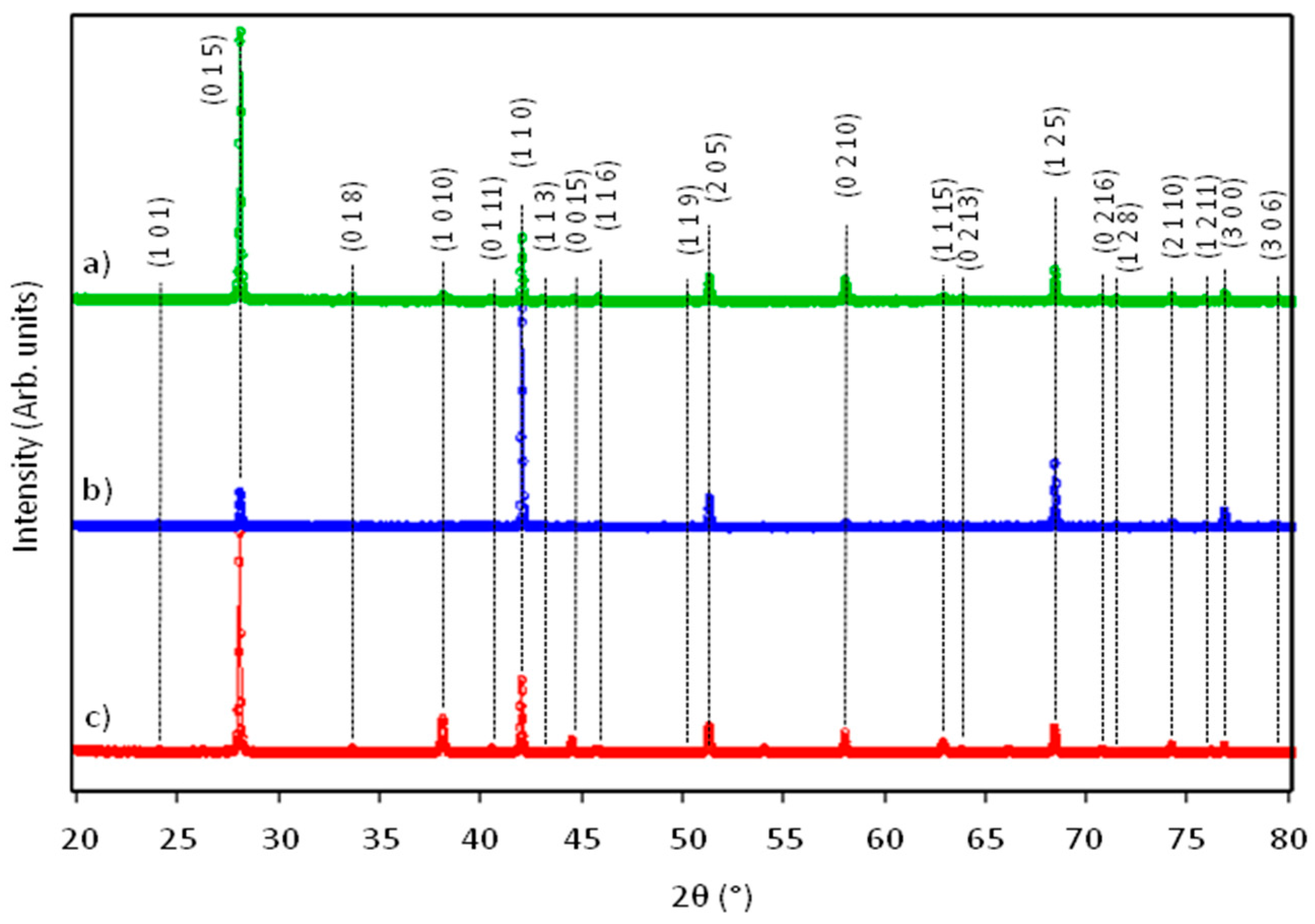
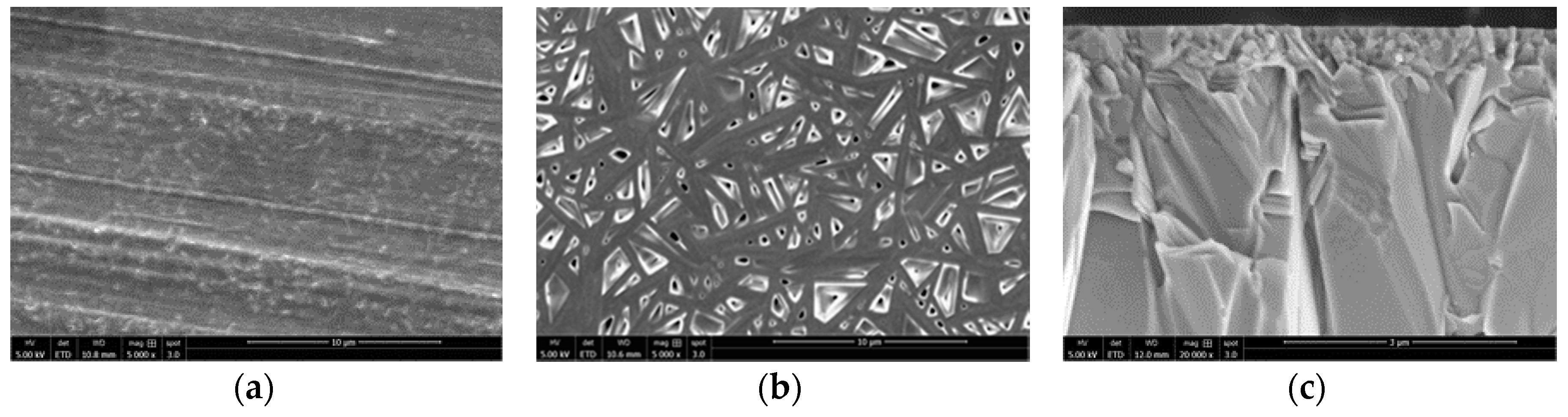
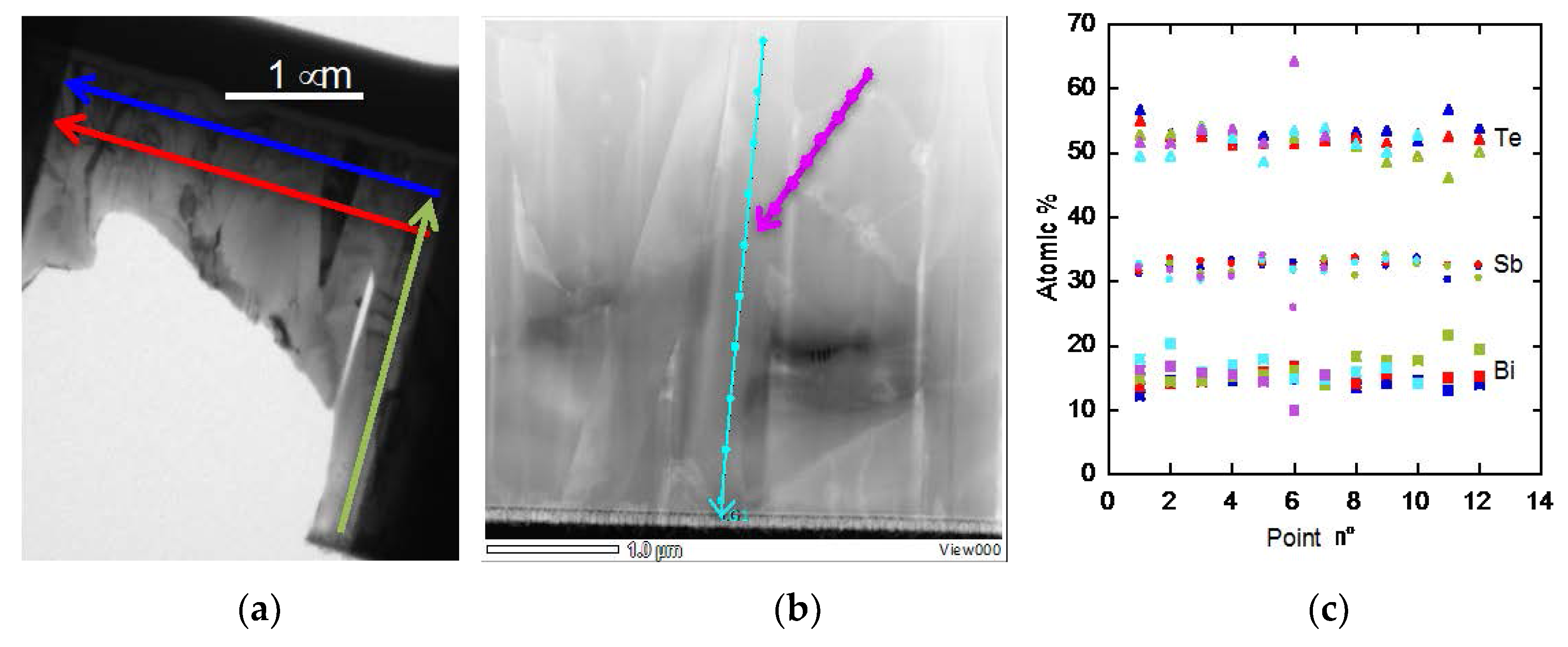
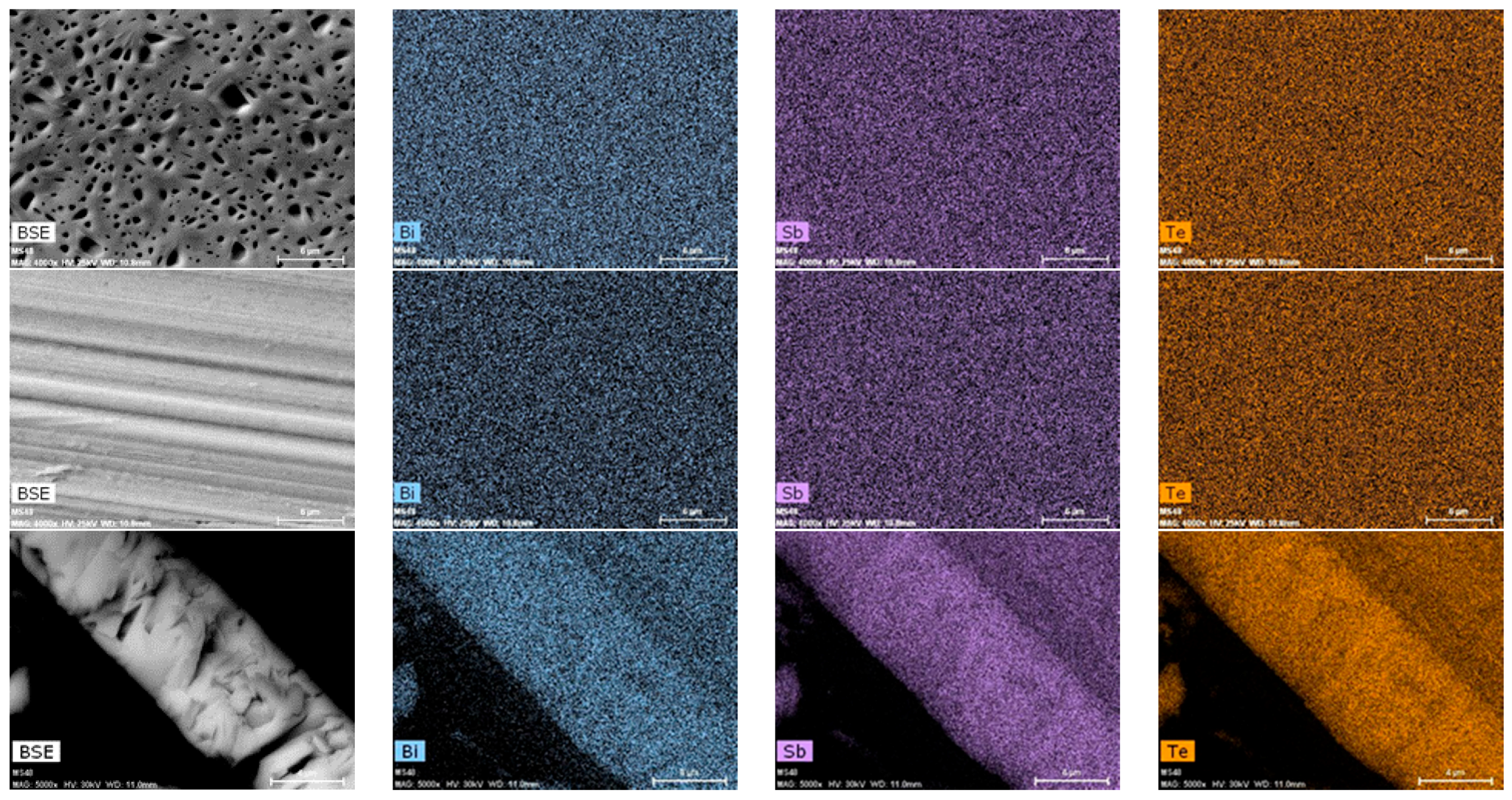
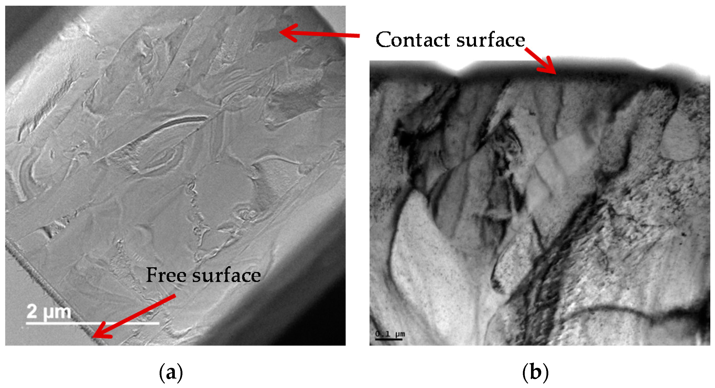
3.1. X-ray Diffraction and Scanning Electron Microscopy

Figure 1 shows the XRD patterns collected on ground ribbons, as well as on the surface in contact with the copper wheel and the free surface. The patterns show that the ribbons are well crystallized regardless of the sample considered. No significant peak broadening is observed suggesting that the grain size is above the nanoscale range. All of the reflections for the ground ribbons and free surface can be indexed with the standard polycrystalline pattern of Bi0.48Sb1.52Te3 indicating the absence of impurity phases. If the patterns of those samples are quite similar, that of the contact surface clearly exhibits a significant degree of texturing along the (110), (015) and (125) planes, indicating an orientation effect during the material’s solidification. The trigonal axis of the crystallites orientated along these three directions forms an angle of 90°, 58°45′ and 77°4′ respectively, with the normal of the free surface as shown in Figure 2. As the XRD pattern of the free surface is similar to that of ground ribbons, the level of texturing should be limited to a region close to the contact surface. Our results are however quite different from those obtained by Koukarenko et al. [46], who studied in detail the texture formation in Bi2Te3 ribbons. Their investigation revealed a well-defined (025) texture independent of the quenching temperature, the ribbon thickness and the heat treatment. This (025) texture was proposed to be correlated to the nature of the Bi-Te covalent bond in this plane. Further investigations on the Bi2−xSbxTe3 (0 ≤ x ≤ 1) system by the same authors showed that substituting Sb for Bi tends to lessen the (025) texture and favors the appearance of the (110) texture [48]. The difference between the textures observed in [46] and in our case could be linked to different cooling rates since the thickness of the ribbons obtained in their studies was significantly higher (between 20 and 35 µm).
The obtained microstructures observed by SEM are similar to those observed in prior studies on similar or close compositions (Figure 3) [37,38,39,43,58]. Typically, top views of the contact surface do not demonstrate any specific microstructural details except those related to the wheel roughness (Figure 3a), while top views of the free surface exhibit what Xie et al. [37,38,39,43] called a dendritic-like microstructure (or a needle network microstructure, as termed by Koukarenko et al. [46,48]) of 0.1–0.5 µm in width (Figure 3b). Cross-section views of the ribbons, shown in Figure 3c, indicate a close-packed microstructure of about some hundreds of nanometers in thickness in the region close to the contact surface, which is composed of a mixture of small-sized particles up to one micrometer in size and possibly of nanosized particles as expected from the MS process. This structure is followed by a columnar growth of the basal planes giving rise to a dendritic or a needle-like appearance of the free surface. According to the XRD results, preferential growth occurs in the thin close-packed microstructure, while an erratic growth takes place in the columnar structure.
The spatial distribution of the elements has been assessed by elemental X-ray mapping on the free and contact surfaces, as well as on a cross-section of the ribbons (Figure 4). At the scale probed by these experiments, all of the elements appear homogeneously distributed within the ribbon. The atomic composition determined by EDXS Bi0.4Sb1.6Te3.0 is very close to the expected composition, given the experimental uncertainty that stems from the strong overlap of the La lines of Te and Sb.

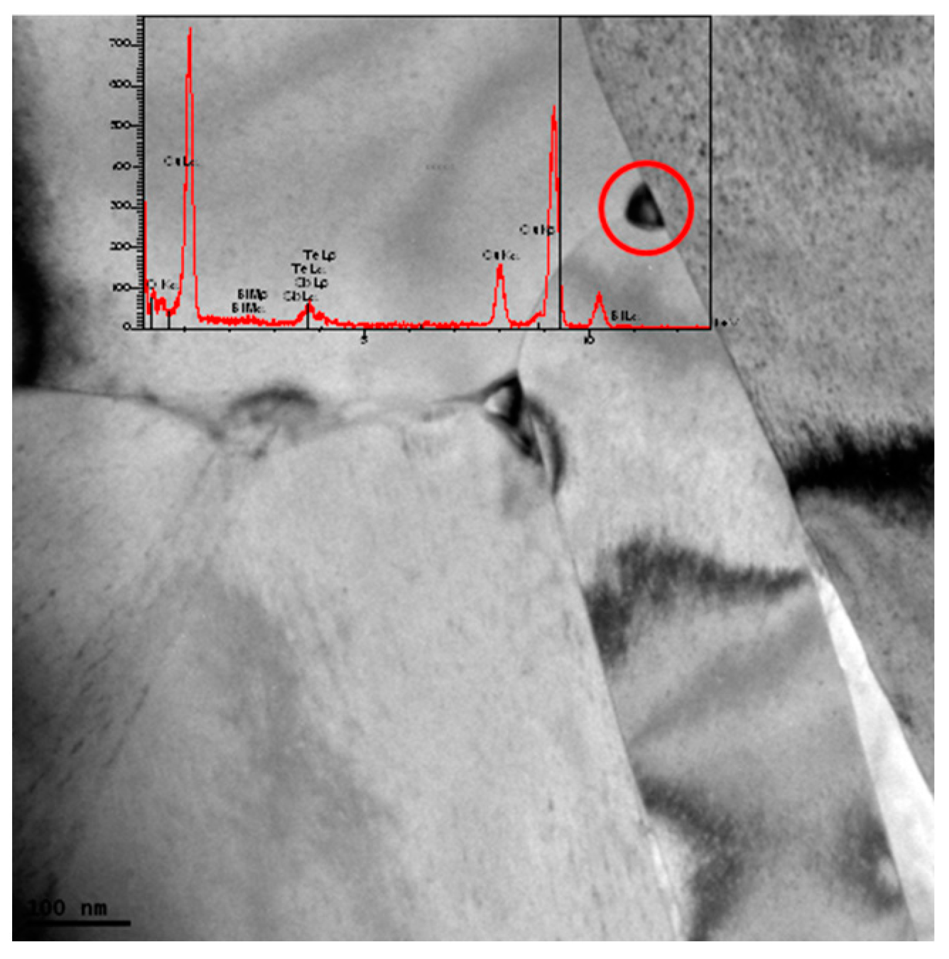
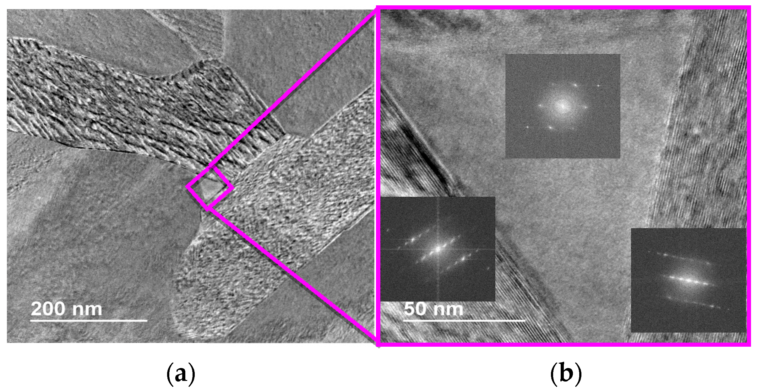
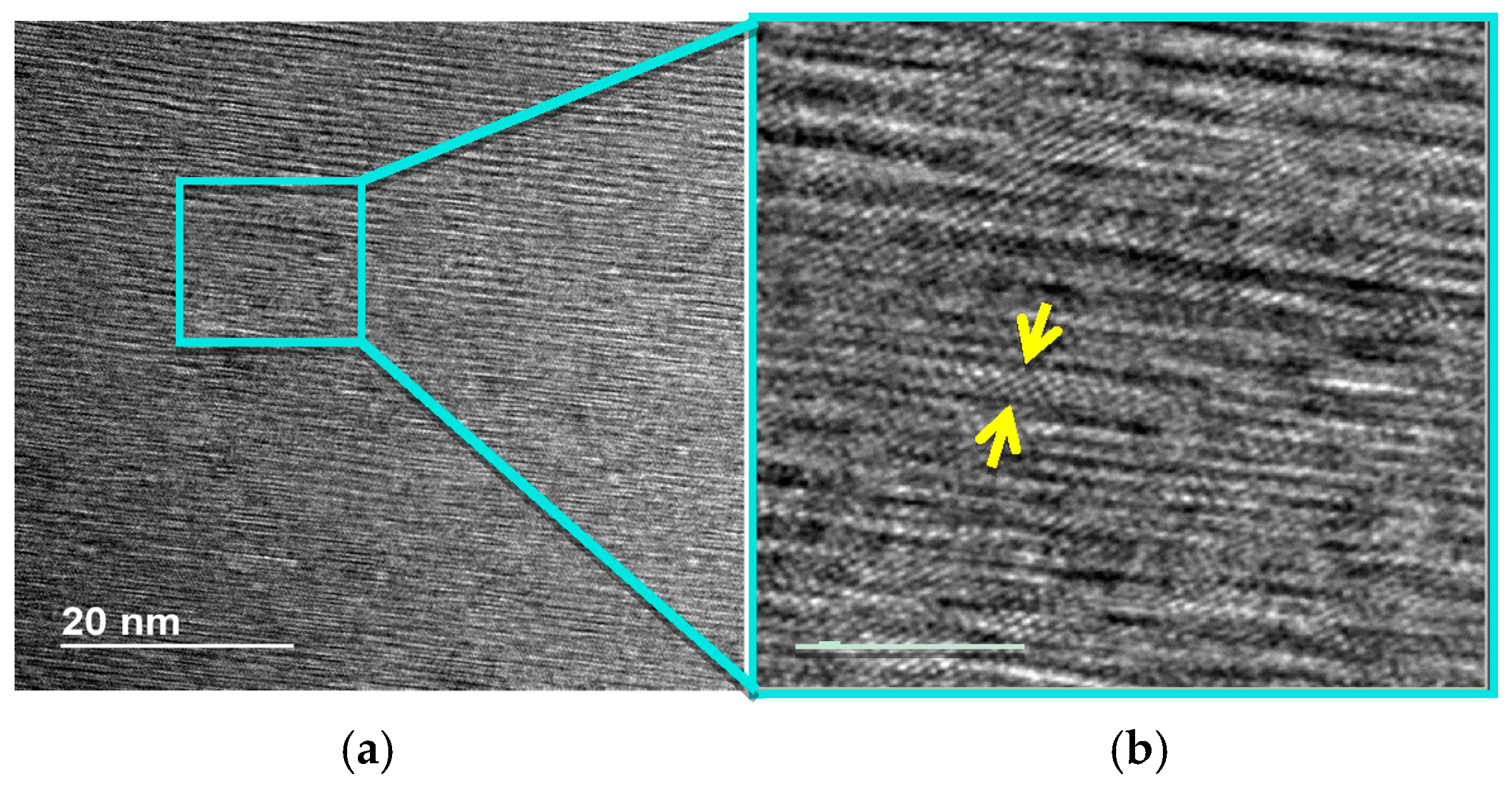
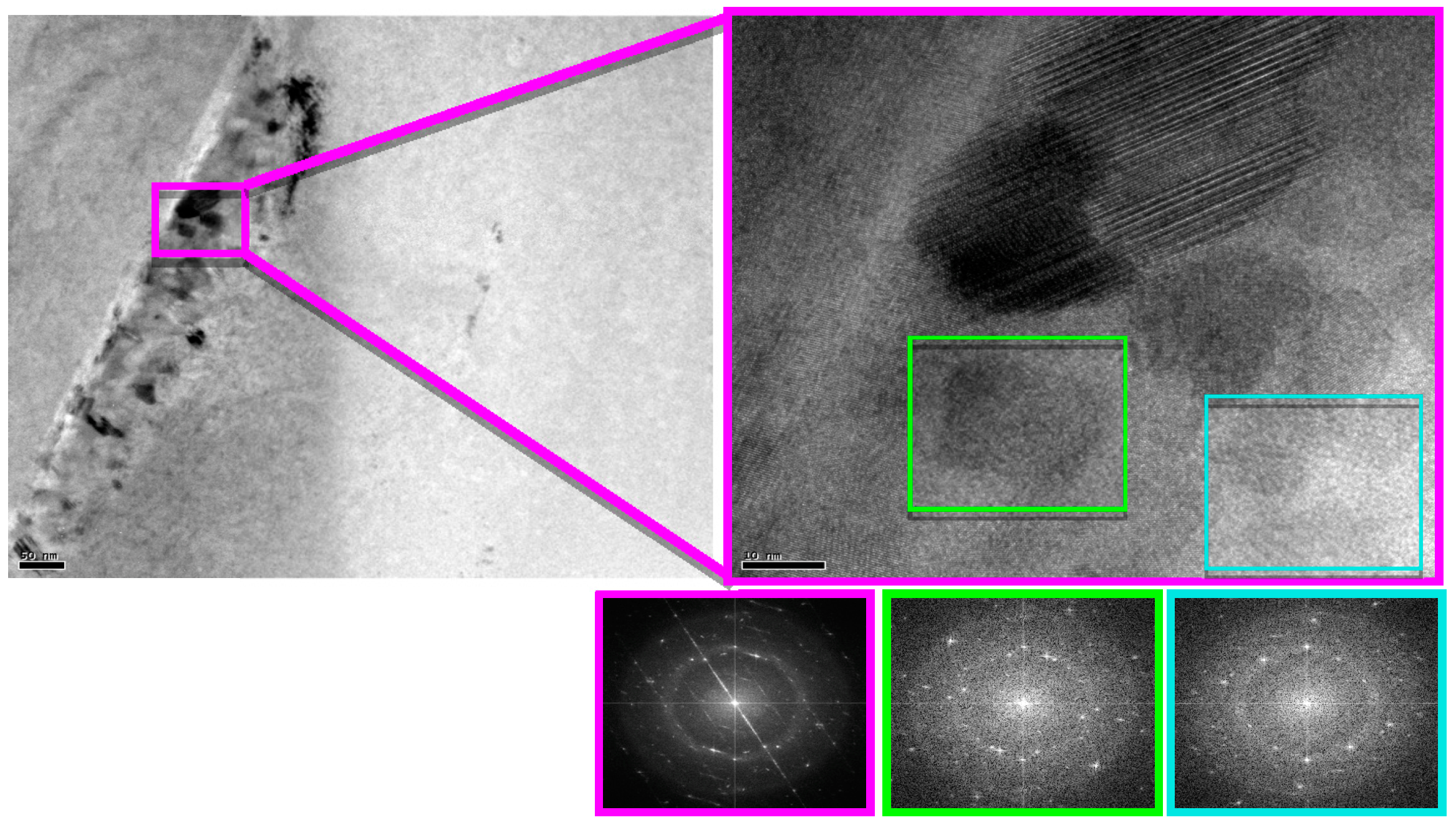
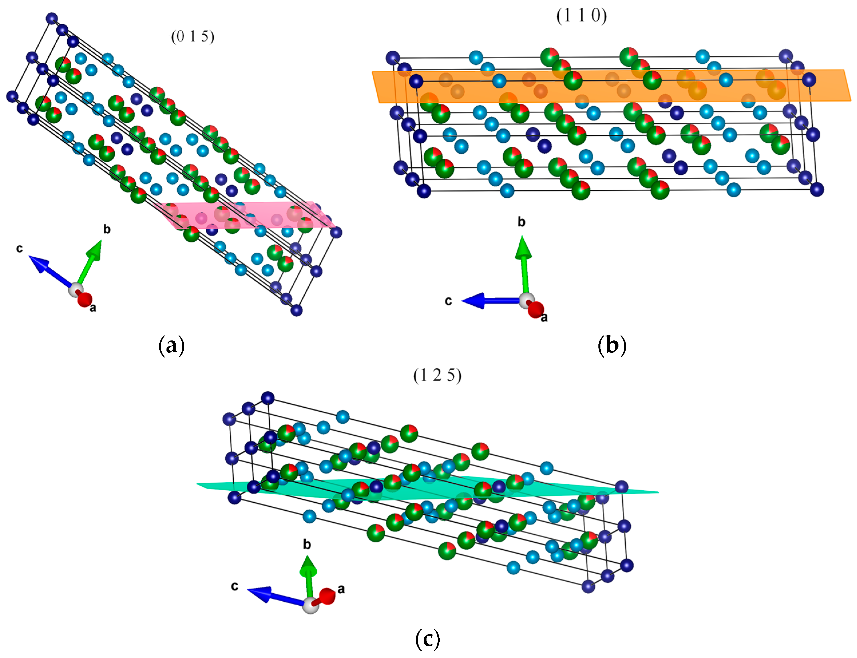
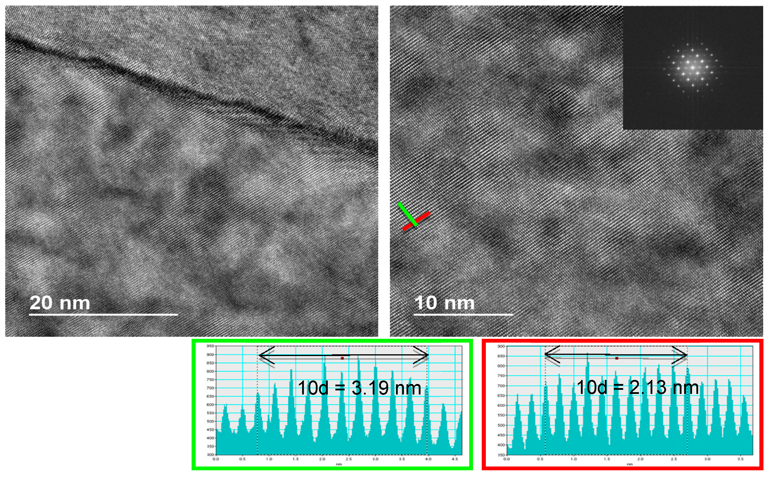
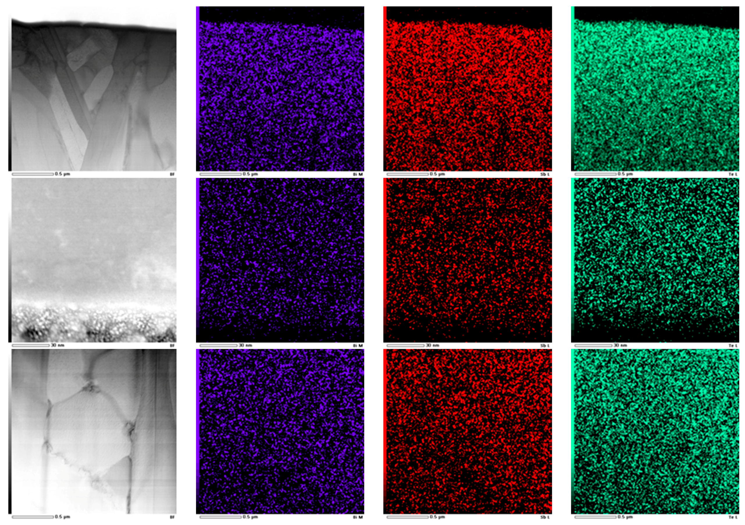
3.2. Transmission Electron Microscopy

TEM and HRTEM studies have been carried out to gain relevant insights into the nanostructure of the ribbons. We address in particular the issues concerning the formation of amorphous zones during the MS process, the presence of which has not been systematically observed in prior studies, and the possible precipitation of elemental Te as observed in single-crystals grown in out-of-equilibrium conditions. A top view obtained by TEM of one of the thin cross-section slices produced by FIB is shown in Figure 5a. Similar features to SEM observations can be seen, that is a close-packed microstructure close to the contact surface of less than 1 μm in thickness followed by a columnar growth. The thickness of the columnar grains is less than 1 μm. The surface close to the wheel is composed of grains of about 100 nm (Figure 5b). In this analyzed section, neither an amorphous, nor a nano-sized zone could be observed. This observation contrasts with the results obtained by Xie et al. [39,42], who found the presence of an amorphous layer of about 500 nm in thickness for an overall thickness of about 3 mm (assuming that the authors showed the entire cross-section). The presence of nanoparticles embedded in an amorphous matrix (thickness of about 1 mm as shown in [39]) could not be observed either. The reasons for these discrepancies remain so far unknown.
Figure 6 displays two HRTEM images collected in the middle zone of a ribbon. The first image was taken at the interface between two grains, while the second image was taken in the center of a grain. Based on the fast Fourier transform (FFT), the grains are well crystallized, and the average inter-fringe distances d taken along the lines in the main and perpendicular directions (0.319 and 0.213 nm, respectively) are in good agreement with the inter-planar distances of the (015) (0.317 nm) and (110) (0.215 nm) planes [59]. These measurements further confirm the orientations found in our XRD analyses. Interestingly, some nano-sized particles of elemental Te could be also observed at grain boundaries as illustrated in Figure 7.
Figure 8 shows a grain boundary between four adjacent grains in the dendritic-like zone obtained from an SEM-FIB thin slice cut parallel to the free surface. The triangular-shaped feature of about 70 nm on the side and located in between larger grains is typical of growth with the trigonal axis perpendicular to the surface evidenced by the hexagonal disposition of the spots obtained on the FFT of this zone. Some of these triangular-shaped structures that exhibit clean surfaces with the surrounding crystals can be observed all over the thin slice. The tops of the two columnar grains surrounding the triangular crystal are single crystalline. Both grains display an interplanar distance of 0.117 nm that corresponds to the (205) planes. Such sub-micron-sized crystalline domains were systematically observed in prior investigations on MS ribbons of BixSb2−xTe3 [37,38,39,42,60].
TEM images also reveal lattice stripes with a larger estimated width of about 10 Å (Figure 9). A magnification of this zone shows that these stripes are formed by a series of five bright-doted rows separated by a more dark-spotted row. This result is consistent with the five-layer lamellae structure of the ideal crystal structure of Sb-Bi tellurides. The above-mentioned width is also in very good agreement with the height of the -Te-Bi-Te-Bi-Te- quintet (12 Å according to [61]). These features are not inherent to the MS process we employed and have also been reported by Lan et al. [62] and Li et al. [63] in p-type BixSb2−xTe3 samples prepared by two synthetic routes consisting of mechanical alloying-SPS and mechanical alloying-hot pressing, respectively. In these two studies, however, the appearance of these stripes was slightly different and was described as a series of two rows of extra-bright dots separated by four weaker bright-dot rows forming the five-layer lamellae.
In addition, we observed a needle-like structure containing nano-grains of about 5–10 nm in size in another thin slice (Figure 10). In contrast to the larger grains, these small grains do not seem to be closely packed. The needle was located in the middle of the cross-section of a ribbon. It is however difficult to determine in this case whether the diffuse halo rings observed in the FFT are due to the MS process or to the small amount of amorphized material produced by the impact of high-energy Ga ions during the FIB sample thinning. We note that we did not observe nanostructures appearing as dense striations with spacing of the order of 10 nm reported in Bi2Te3 by Jacquot et al. [60] and Lan et al. [62] and described in the prior study of Peranio and Eibl [64]. Although these structures could be present as well in our samples, these features may also arise from the preparation of the thin slices by ion-milling with Ar+ ions as underlined by Homer and Medlin [65].
The chemical composition of the ribbons was further analyzed by EDXS using the STEM mode along five profiles on two ribbons as depicted in Figure 11. The compositions seem independent of the region probed, the data taken along a columnar grain (green and sky blue lines) and in the dendritic zone (dark blue and red lines) being roughly similar. X-ray elemental mappings were performed in several zones of one ribbon, that is in the dendritic zone, at the interface of the amorphous-crystallized grains and within a hexagonal grain (Figure 12). The elemental distribution shows that the elements are evenly distributed in the dendrites, the columnar structures and the amorphous layer, without any particular compositional segregation.

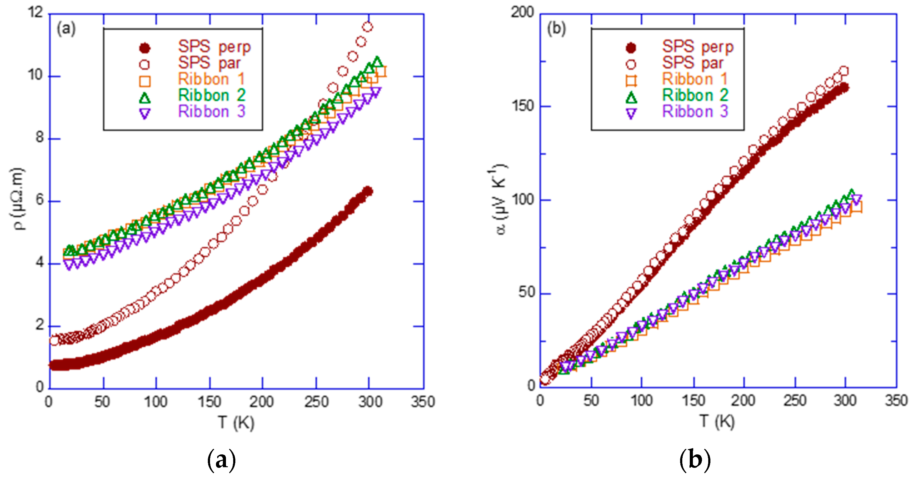
3.3. Transport Properties

Figure 13a shows the temperature dependence of the electrical resistivity ρ of three randomly-selected ribbons along with the data collected on the reference Bi0.48Sb1.52Te3 bulk polycrystalline sample measured parallel and perpendicular to the pressing direction. The ρ values of the bulk sample are constant below 20 K and increase above this temperature with increasing temperature. Above 200 K, ρ roughly follows a T1.5 law. Taking into account the magnitude of ρ (from 1 up to 12 µΩ m), this behavior is typical of heavily-doped semiconductors as expected for the Bi0.48Sb1.52Te3 composition. Consistent with the results obtained on single crystals [23,24], these measurements show a significant difference in the data measured perpendicular and parallel to the pressing direction, the latter of which is higher. Further, the anisotropy ratio defined as:
γ = ρpar/ρperp
is not constant over the whole temperature range, but increases with temperature to reach 1.8 at 300 K. This result indicates that the SPS process induces a preferred orientation, which is parallel to the trigonal axis, along the SPS pressing direction. The ρ(T) data measured on the ribbons show the same general trend with respect to the reference sample. The ρ values fall in between those of the bulk samples with room-temperature values approaching 10 mΩ m. These measurements tend to indicate that the typical microstructure of the ribbons does not significantly affect the electrical transport. Of note is the fact that the three randomly-selected ribbons show similar values to within experimental uncertainty, which evidences that MS is a robust process for producing chemically-homogeneous ribbons with nearly-identical electrical properties.
The thermopower α of the Bi0.48Sb1.52Te3 bulk sample and ribbons is shown in Figure 13b as a function of temperature. All samples exhibit positive α values, which vary linearly below 40 K and logarithmically above 200 K. In agreement with the ρ data, this behavior is consistent with those of heavily-doped semiconductors. Our results obtained on the SPS sample are in line with the well-known fact that α does not depend on the orientation in the extrinsic or one-carrier regime in (Sb2Te3)-(Bi2Te3) solid solutions [2]. No differences in the α values for the three ribbons are visible, confirming their very similar physical properties. Yet, the α values of the ribbons are lower than those of the bulk specimen in the whole temperature range. This behavior is likely related to a change of either the carrier concentration and/or the scattering parameter due to the MS process. Measurement of the Hall coefficient RH reveals that the apparent Hall concentration pH differs significantly at 300 K for the bulk sample and the ribbons (Table 1). The hole concentration measured in the ribbons is almost two-times higher than in the bulk, indicative of the more pronounced metallic character of the ribbons. Thus, the very good agreement between the electrical resistivity observed in the SPS samples and in the ribbons is only fortuitous and is a direct consequence of the increased hole concentration that compensates the decrease in the Hall mobility µH (Table 1). The degradation of µH is likely linked to the numerous interfaces at the microscale length present along the current direction, as evidenced by microscopic analyses, which efficiently scatter holes. Note that a more metallic state has also been observed at 300 K in BixSb2−xTe3 ribbons for x = 0.40 [48]. In these prior investigations, the melt-spinning technique was shown to produce homogeneous ribbons with identical electrical properties although the intrinsic properties of the carriers (concentration and mobility) are different from those of the bulk SPS samples. The excellent reproducibility of the transport properties in Bi0.48Sb1.52Te3 ribbons observed herein thus confirms the conclusions drawn for analogous compounds [43,44,45,46,47,48,49,60].
Finally, it should be kept in mind that the electronic properties of mixed crystals based on Sb2Te3-Bi2Te3 are governed by native defects, the influence of which outweighs the role of differences in the microstructure of the samples. In Sb-rich Sb2Te3-Bi2Te3 compositions, antistructure defects are the main type of defects with Sb (and partially Bi) atoms replacing Te atoms, which are usually denoted SbTe (or BiTe). The SbTe defects are electrically active and behave as single acceptors giving rise to p-type electrical conduction [66,67]. The presence of native defects prevents the solid solution from being stoichiometric, that is the higher the defect concentration, the higher the deviation from stoichiometry. Controlling these deviations, and hence the electrical properties, is the main challenge to overcome for optimizing the thermoelectric properties of these compounds. In this context, the precise knowledge of the phase diagram can be a powerful tool to properly control the carrier concentration. The solidus line, characterizing the maximum deviation from stoichiometry, was investigated in the past in the Te and Sb rich-side of the Sb2−xBixTe3 (x = 0.0, 0.4 and 0.5) solid solution at the thermodynamic equilibrium [2,23]. However, for non-equilibrium processes, the phase diagram can be severely affected as demonstrated in prior studies [17,68]. These works showed that in fast-cooling processes, Te exhibits a retrograde solubility and thus tends to precipitate out of the main phase, in agreement with our TEM observations. Since a lower Te content in the matrix contributes to further enhancing the deviations from stoichiometry, it results in an increased hole concentration due to the triple-acceptor nature of Te vacancies [67]. The slight Te precipitation is thus likely at the origin of the increased hole concentration we observe in melt-spun ribbons.

4. Conclusions

p-type Bi0.48Sb1.52Te3 ribbons have been synthesized successfully via melt-spinning. Our detailed structural and chemical characterizations have confirmed that this technique enables achieving excellent chemical homogeneity and reproducibility. TEM studies carried out on ribbons revealed the very different microstructure exhibited by the free surface and the surface in direct contact with the copper wheel. The very high cooling rates achieved with this technique have a sizeable influence on the transport properties of the ribbons that exhibit a more metallic nature compared to bulk samples of the same initial composition prepared from a conventional synthesis route. Variations in deviations from stoichiometry, which are known to play a prominent role in this family of compounds, likely explain this difference. These results provide a good basis to better understand the variations in the transport properties of p-type BixSb2−xTe3 compounds at various steps of the synthetic process used to produce bulk samples from melt-spun ribbons. Extending these investigations to other compositions would be of interest to determine whether melt-spinning leads to enhanced thermoelectric performances in Bi2Te3-based solid solutions.

Acknowledgments

This work was supported by Electricité de France R&D through the CIFRE (Conventions Industrielles de Formation par la Recherche), convention No. 2011/1329. The authors thank Pascal Dalicieux, Philippe Baranek and Laurent Legras from Electricité de France. They are also grateful to Jaafar Ghanbaja for his support in HRTEM investigations.

Author Contributions

B.L. conceived of and designed the experiments. V.O. performed the experiments, prepared all of the samples for characterizations and transport properties measurements and analyzed the data. S.M. and A.D. performed the TEM investigations. A.D. carried out SEM experiments. E.B.L. performed the measurements on the ribbons. V.O., B.L. and C.C. wrote the paper.

Conflicts of Interest

The authors declare no conflict of interest. The founding sponsors had no role in the design of the study; in the collection, analyses or interpretation of data; in the writing of the manuscript; nor in the decision to publish the results.

References

  1. Goldsmid, H.J. Thermoelectric Refrigeration; The International Cryogenics Monograph Series; Plenum Press: New York, NY, USA, 1964. [Google Scholar]
  2. Rowe, D.M. Thermoelectrics and Its Energy Harvesting; CRC Press: Boca Raton, FL, USA, 2012. [Google Scholar]
  3. Snyder, G.J.; Toberer, E.S. Complex thermoelectric materials. Nat. Mater. 2008, 7, 105–114. [Google Scholar] [CrossRef] [PubMed]
  4. Brown, S.R.; Kauzlarich, S.M.; Gascoin, F.; Snyder, G.J. Yb14MnSb11: New high efficiency thermoelectric material for power generation. Chem. Mater. 2006, 18, 1873–1877. [Google Scholar] [CrossRef]
  5. Zhang, H.; Borrmann, H.; Oeschler, N.; Candolfi, C.; Schnelle, W.; Schmidt, M.; Burkhardt, U.; Baitinger, M.; Zhao, J.T.; Grin, Y. Atomic interactions in the p-type clathrate I Ba8Au5.3Ge40.7. Inorg. Chem. 2011, 50, 1250–1257. [Google Scholar] [CrossRef] [PubMed]
  6. Shi, X.; Yang, J.; Bai, S.; Yang, J.; Wang, H.; Chi, M.; Salvador, J.R.; Zhang, W.; Chen, L.; Wong-Ng, W. On the design of high-efficiency thermoelectric clathrates through a systematic cross-substitution of framework elements. Adv. Funct. Mater. 2010, 20, 755–763. [Google Scholar] [CrossRef]
  7. Toberer, E.S.; Zevalkink, A.; Crisosto, N.; Snyder, G.J. The zintl compound Ca5Al2Sb6 for low-cost thermoelectric power generation. Adv. Funct. Mater. 2010, 20, 4375–4380. [Google Scholar] [CrossRef]
  8. Gougeon, P.; Gall, P.; Al Rahal Al Orabi, R.; Fontaine, B.; Gautier, R.; Potel, M.; Zhou, T.; Lenoir, B.; Colin, M.; Candolfi, C.; et al. Synthesis, crystal and electronic structures, and thermoelectric properties of the novel cluster compound Ag3In2Mo15Se19. Chem. Mater. 2012, 24, 2899–2908. [Google Scholar] [CrossRef]
  9. Al Rahal Al Orabi, R.; Gougeon, P.; Gall, P.; Fontaine, B.; Gautier, R.; Colin, M.; Candolfi, C.; Dauscher, A.; Hejtmanek, J.; Malaman, B.; et al. X-ray characterization, electronic band structure, and thermoelectric properties of the cluster compound Ag2Tl2Mo9Se11. Inorg. Chem. 2014, 53, 11699–11709. [Google Scholar] [CrossRef] [PubMed]
  10. Kurosaki, K.; Yamanaka, S. Low-thermal-conductivity group 13 chalcogenides as high-efficiency thermoelectric materials. Phys. Status Solidi A 2013, 210, 82–88. [Google Scholar] [CrossRef]
  11. Lu, X.; Morelli, D.T.; Xia, Y.; Zhou, F.; Ozolins, V.; Chi, H.; Zhou, X.; Uher, C. High performance thermoelectricity in earth-abundant compounds based on natural mineral tetrahedrites. Adv. Energy Mater. 2013, 3, 342–348. [Google Scholar] [CrossRef]
  12. Suekuni, K.; Kim, F.S.; Nishiate, H.; Ohta, M.; Tanaka, H.I.; Takabatake, T. High-performance thermoelectric minerals: Colusites Cu26V2M6S32 (M = Ge, Sn). Appl. Phys. Lett. 2014, 105, 132107. [Google Scholar] [CrossRef]
  13. Zhang, H.; Liu, C.X.; Qi, X.L.; Dai, X.; Fang, Z.; Zhang, S.C. Topological insulators in Bi2Se3, Bi2Te3 and Sb2Te3 with a single dirac cone on the surface. Nature Phys. 2009, 5, 438–442. [Google Scholar] [CrossRef]
  14. Xia, Y.; Qian, D.; Hsieh, D.; Wray, L.; Pal, A.; Lin, H.; Bansil, A.; Grauer, D.; Hor, Y.S.; Cava, R.J.; et al. Observation of a large-gap topological-insulator class with a single dirac cone on the surface. Nat. Phys. 2009, 5, 398–402. [Google Scholar] [CrossRef]
  15. Ando, Y. Topological insulator materials. J. Phys. Soc. Jpn. 2013, 82, 102001. [Google Scholar] [CrossRef]
  16. Paglione, J.; Butch, N.P. Growth and characterization of topological insulators. In Topological Insulators, Fundamentals and Perspectives; Ortmann, F., Roche, S., Valenzuela, S.O., Eds.; Wiley-VCH Verlag GmbH & Co., KGaA: Weinheim, Germany, 2015; pp. 245–262. [Google Scholar]
  17. Abrikosov, N.K.; Bankina, V.F.; Kolomoets, L.A.; Dzhaliashvili, N.V. Deviation of the solid solution from stoichiometry in the section Bi2Te3–Sb2Te3 in the region of Bi0.5Sb1.5Te3 composition. Izv. Akad. Nauk. SSSR Neorg. Mater. 1977, 13, 827–829. (In Russian) [Google Scholar]
  18. Barash, A.S.; Zhukova, T.B.; Parparov, E.Z. Structure and thermoelectric properties of Bi2Te3-xSex and Bi0,25Sb1,48Te3. Izv. Akad. Nauk. SSSR Neorg. Mater. 1976, 12, 1552. (In Russian) [Google Scholar]
  19. Rosi, F.D.; Abeles, B.; Jensen, R.V. Materials for thermoelectric refrigeration. J. Phys. Chem. Solids 1959, 10, 191–200. [Google Scholar] [CrossRef]
  20. Susmann, H.; Loof, K. Copper doping and dislocations in the system Bi2Te3–Sb2Te3. Phys. Stat. Sol. A 1976, 37, 467–471. (In German) [Google Scholar]
  21. Volotskii, M.P. Investigation of the complex structure of band edges and of the mechanism of carrier scattering in Bi-Sb-Te single crystals. Fiz. Tekh. Polupr. SSSR 1974, 8, 1044. (In Russian) [Google Scholar]
  22. Yim, W.M.; Amith, A. Bi–Sb alloys for magneto-thermoelectric and thermomagnetic cooling. Solid-State Electron. 1972, 15, 1141–1144. [Google Scholar] [CrossRef]
  23. Caillat, T.; Carle, M.; Perrin, D.; Scherrer, H.; Scherrer, S. Study of the Bi–Sb–Te phase diagram. J. Phys. Chem. Solids 1992, 53, 227–232. [Google Scholar] [CrossRef]
  24. Caillat, T.; Carle, M.; Pierrat, P.; Scherrer, H.; Scherrer, S. Thermoelectric properties of (BixSb1−x)2Te3 single crystal solid solutions grown by the THM method. J. Phys. Chem. Solids 1992, 53, 1121–1129. [Google Scholar] [CrossRef]
  25. Qinghui, J.; Junyou, Y.; Yong, L.; Hongcai, H. Microstructure tailoring in nanostructured thermoelectric materials. J. Adv. Dielect. 2016, 6, 1630002. [Google Scholar]
  26. Fan, X.A.; Yang, J.Y.; Chen, R.G.; Yun, H.S.; Zhu, W.; Bao, S.Q.; Duan, X.K. Characterization and thermoelectric properties of p-type 25%Bi2Te3–75%Sb2Te3 prepared via mechanical alloying and plasma activated sintering. J. Phys. D Appl. Phys. 2006, 39, 740–745. [Google Scholar] [CrossRef]
  27. Vasilevskiy, D.; Dawood, M.S.; Masse, J.P.; Turenne, S.; Masut, R.A. Generation of nanosized particles during mechanical alloying and their evolution through the hot extrusion process in bismuth-telluride-based alloys. J. Electron. Mater. 2010, 39, 1890–1896. [Google Scholar] [CrossRef]
  28. Navratil, J.; Starý, Z.; Plechacek, T. Thermoelectric properties of p-type antimony bismuth telluride alloys prepared by cold pressing. Mater. Res. Bull. 1996, 31, 1559–1566. [Google Scholar] [CrossRef]
  29. Yamashita, O.; Tomiyoshi, S.; Makita, K. Bismuth telluride compounds with high thermoelectric figures of merit. J. Appl. Phys. 2003, 93, 368–374. [Google Scholar] [CrossRef]
  30. Pierrat, P.; Dauscher, A.; Lenoir, B.; Martin-Lopez, R.; Scherrer, H. Preparation of the Bi8Sb32Te60 solid solution by mechanical alloying. J. Mater. Sci. 1997, 32, 3653–3657. [Google Scholar] [CrossRef]
  31. Martin-Lopez, R.; Lenoir, B.; Dauscher, A.; Scherrer, H.; Scherrer, S. Preparation of n-type Bi–Sb–Te thermoelectric material by mechanical alloying. Solid State Commun. 1998, 108, 285–288. [Google Scholar] [CrossRef]
  32. Glazov, V.M.; Yatmanov, Y.V. Thermoelectric properties of Bi2Te2.4Se0.6 and Bi0.52Sb1.48Te3 semiconductor solid solutions prepared by ultrarapid liquid quenching. Izv. Akad. Nauk. SSSR Neorg. Mater. 1986, 22, 36–40. (In Russian) [Google Scholar]
  33. Glazov, V.M.; Potemkin, A.Y.; Akopyan, R.A. Preparation of homogeneous inorganic solid solutions by diffusionless solidification. Izv. Akad. Nauk. SSSR Neorg. Mater. 1996, 32, 1461–1465. (In Russian) [Google Scholar]
  34. Gogishvili, O.S.; Lalikin, S.P.; Krivoruchko, S.P.; Pyrychidi, K.I.; Zanava, E.S. Synthesis of alloys based on chalcogenides of Bi and Sb by ultra-fast quenching method. In Proceedings of the VII Chemistry, Physics and Technical Application of Chalcogenides, Uzhhorod, Ukraine, 24–27 October 1988; p. 368. (In Russian). [Google Scholar]
  35. Gogishvili, O.S.; Kononov, G.G.; Krivoruchko, S.P.; Lavrinenko, I.P.; Ovsyanko, I.I. Structural study of (Bi,Sb)2Te3 alloys synthesized by quenching from the liquid state. Izv. Akad. Nauk SSSR Neorg. Mater. 1991, 27, 923. (In Russian) [Google Scholar]
  36. Dreglea, A. Boundary-Value Problems in Melt Spinning Modeling: Analytical and Numerical Methods; Lambert Acad. Publ. GmbH & Co., KG: Saarbrucken, Germany, 2012. [Google Scholar]
  37. Xie, W.; Tang, X.; Yan, Y.; Zhang, Q.; Tritt, T.M. High thermoelectric performance BiSbTe alloy with unique low-dimensional structure. J. Appl. Phys. 2009, 105, 113713. [Google Scholar] [CrossRef]
  38. Xie, W.; Tang, X.; Yan, Y.; Zhang, Q.; Tritt, T.M. Unique nanostructures and enhanced thermoelectric performance of melt-spun BiSbTe alloys. Appl. Phys. Lett. 2009, 94, 102111. [Google Scholar] [CrossRef]
  39. Xie, W.; He, J.; Kang, H.J.; Tang, X.; Zhu, S.; Laver, M.; Wang, S.; Copley, J.R.D.; Brown, C.M.; Zhang, Q.; et al. Identifying the specific nanostructures responsible for the high thermoelectric performance of (Bi,Sb)2Te3 nanocomposites. Nano Lett. 2010, 10, 3283–3289. [Google Scholar] [CrossRef] [PubMed]
  40. Xie, W.J.; He, J.; Zhu, S.; Su, X.L.; Wang, S.Y.; Holgate, T.; Graff, J.W.; Ponnambalam, V.; Poon, S.J.; Tang, X.F.; et al. Simultaneously optimizing the independent thermoelectric properties in (Ti,Zr,Hf)(Co,Ni)Sb alloy by in situ forming InSb nanoinclusions. Acta Mater. 2010, 58, 4705–4713. [Google Scholar] [CrossRef]
  41. Xie, W.; He, J.; Zhu, S.; Holgate, T.; Wang, S.; Tang, X.; Zhang, Q.; Tritt, T.M. Investigation of the sintering pressure and thermal conductivity anisotropy of melt-spun spark-plasma-sintered (Bi,Sb)2Te3 thermoelectric materials. J. Mater. Res. 2011, 26, 1791–1799. [Google Scholar] [CrossRef]
  42. Xie, W.; Wang, S.; Zhu, S.; He, J.; Tang, X.; Zhang, Q.; Tritt, T.M. High performance Bi2Te3 nanocomposites prepared by single-element-melt-spinning spark-plasma sintering. J. Mater. Sci. 2013, 48, 2745–2760. [Google Scholar] [CrossRef]
  43. Ivanova, L.D.; Petrova, L.I.; Granatkina, Y.V.; Leontyev, V.G.; Ivanov, A.S.; Varlamov, S.A.; Prilepo, Y.P.; Sychev, A.M.; Chuik, A.G.; Bashkov, I.V. Thermoelectric and mechanical properties of the Bi0.5Sb1.5Te3 solid solution prepared by melt spinning. Inorg. Mater. 2013, 49, 120–126. [Google Scholar] [CrossRef]
  44. Koukharenko, E.; Frety, N.; Shepelevich, V.G.; Tedenac, J.C. Thermoelectric properties of Bi2Te3 material obtained by the ultrarapid quenching process route. J. Alloys Compd. 2000, 299, 254–257. [Google Scholar] [CrossRef]
  45. Koukharenko, E.; Vassilev, G.P.; Nancheva, N.; Docheva, P.; Tedenac, J.C.; Frety, N.; Shepelevich, V.G. defects in Sb2−xBixTe3 foils. J. Alloys Compd. 1999, 287, 239–242. [Google Scholar] [CrossRef]
  46. Koukharenko, E.; Frety, N.; Nabias, G.; Shepelevich, V.G.; Tedenac, J.C. Microstructural study of Bi2Te3 material obtained by ultrarapid quenching process route. J. Cryst. Growth 2000, 209, 773–778. [Google Scholar] [CrossRef]
  47. Koukharenko, E.; Shepelevich, V.G. Structural and thermoelctric properties of rapidly quenched Bi2−xSbxTe foils. Inorg. Mater. 1999, 35, 115–117. [Google Scholar]
  48. Koukharenko, E.; Frety, N.; Shepelevich, V.G.; Tedenac, J.C. Microstructure and thermoelectric properties of thin foils of bismuth telluride alloys. Mater. Res. Soc. Symp. Proc. 1999, 545, 507–512. [Google Scholar] [CrossRef]
  49. Koukharenko, E.; Frety, N.; Shepelevich, V.G.; Tedenac, J.C. Electrical and microstructural properties of Bi2−xSbxTe and Bi2−xSbxTe2 foils obtained by the ultrarapid quenching process. J. Mater. Sci. Mater. Electron. 2003, 14, 383–388. [Google Scholar] [CrossRef]
  50. Ohorodniichuk, V.; Candolfi, C.; Masschelein, P.; Baranek, P.; Dalicieux, P.; Dauscher, A.; Lenoir, B. Influence of preparation processing on the transport properties of melt-spun Sb2−xBixTe3+y. J. Electron. Mater. 2016, 45, 1561–1569. [Google Scholar] [CrossRef]
  51. Huang, S.C.; Laforce, R.; Ritter, A.; Goehner, R. Rapid solidification characteristics in melt-spinning a Ni-base superalloy. Met. Trans. A 1985, 16, 1773–1779. [Google Scholar] [CrossRef]
  52. Fedotov, A.S.; Svito, I.A.; Gusakova, S.V.; Shepelevich, V.G.; Saad, A.; Mazanik, A.V.; Fedotov, A.K. Electronic properties of Bi-Sn diluted alloys. Mater. Today 2014, 2, 629–636. [Google Scholar] [CrossRef]
  53. Boettinger, W.J.; Perepezko, J.H. Rapidly Solidified Alloys: Processes, Structures, Properties, Applications; Liebermann, H.H., Ed.; Marcel Dekker Inc.: New York, NY, USA, 1993. [Google Scholar]
  54. Birkholz, M. Thin Film Analysis by X-ray Scattering; John Wiley & Sons: Somerset, NJ, USA, 2006. [Google Scholar]
  55. Creagh, D.C.; Hubbell, J.H. X-ray absorption (or attenuation) coefficients. In International Tables for Crystallography C; Wilson, A.J.C., Prince, E., Kluwer, D., Eds.; Kluwer Academic Publishers: Dordrecht, The Netherlands, 1999; p. 220. [Google Scholar]
  56. Almeida, M.; Alcácer, L.; Oostra, S. Anisotropy of Thermopower in N-methyl-N-ethylmorpholinium bistetracyanoquinodimethane, MEM(TCNQ)2 in the Region of the High-Temperature Phase Transitions. Phys. Rev. B 1984, 30, 2839–2844. [Google Scholar] [CrossRef]
  57. Huebener, H.P. Thermoelectric Power of Lattice Vacancies of Gold. Phys. Rev. 1964, 135, A1281–A1291. [Google Scholar] [CrossRef]
  58. Ohorodniichuk, V.; Dauscher, A.; Masschelein, P.; Candolfi, C.; Baranek, P.; Dalicieux, P.; Lenoir, B. Influence of the nozzle diameter as a control parameter of the properties of melt-spun Sb2−xBixTe3. J. Electron. Mater. 2016, 45, 1419–1424. [Google Scholar] [CrossRef]
  59. Ivanov, L.D.; Kop’ev, I.M.; Lobzov, M.A.; Abrikosov, N.K. Mechanical properties of sngle-crystals of solid solutions of the system Sb1.5Bi0.5Te3–Bi2Se3. Inorg. Mater. 1987, 23, 1288–1291. [Google Scholar]
  60. Jacquot, A.; Vollmer, F.; Bayer, B.; Jaegle, M.; Ebling, D.G.; Böttner, H. Thermal conductivity measurements on challenging samples by the 3-omega method. J. Electron. Mater. 2010, 39, 1621–1626. [Google Scholar] [CrossRef]
  61. Goltsman, B.M.; Kudinov, V.A.; Smirnov, I.A. Semiconductor Thermoelectric Materials Based on Bi2Te3 (Nauka, Moscow, 1972); Army Foreign Science and Technology Center: Charlottesville, VA, USA, 1973. [Google Scholar]
  62. Lan, Y.; Poudel, B.; Ma, Y.; Wang, D.; Dresselhaus, M.S.; Chen, G.; Ren, Z. Structure study of bulk nanograined thermoelectric bismuth antimony telluride. Nano Lett. 2009, 9, 1419–1422. [Google Scholar] [CrossRef] [PubMed]
  63. Li, G.; Gadelrab, K.R.; Souier, T.; Potapov, P.L.; Chen, G.; Chiesa, M. Mechanical properties of BixSb2−xTe3 nanostructured thermoelectric material. Nanotechnology 2012, 23, 065703. [Google Scholar] [CrossRef] [PubMed]
  64. Peranio, N.; Eibl, O. Structural modulations in Bi2Te3. J. Appl. Phys. 2008, 103, 024314. [Google Scholar] [CrossRef]
  65. Homer, M.D.; Medlin, L. Preparation Methods for TEM Specimens of Bismuth Telluride and Related Thermoelectric Alloys. Microsc. Microanal. 2012, 18, 1482–1500. [Google Scholar] [CrossRef]
  66. Thonhauser, T.; Jeon, G.S.; Mahan, G.D.; Sofo, J.O. Stress-induced defects in Sb2Te3. Phys. Rev. B 2003, 68, 205207. [Google Scholar] [CrossRef]
  67. Pecheur, P.; Toussaint, G. Tight-binding studies of crystal stability and defects in Bi2Te3. J. Phys. Chem. Solids 1994, 55, 327–338. [Google Scholar] [CrossRef]
  68. Manyakin, S.M.; Volkov, M.P. Microstructure of (Bi0.25Sb0.75)2Te3 Profiled Crystals Grown by Directed Crystallization Method. In Proceedings of the Twenty-First International Conference on Thermoelectrics, Long Beach, CA, USA, 25–29 August 2002; pp. 21–23. [Google Scholar]
Figure 1. XRD patterns of the free surface (a), contact surface (b) and ground ribbons (c) of melt-spun Bi0.48Sb1.52Te3.
Crystals 07 00172 g001
Figure 2. Scheme of the most pronounced orientations depending on the surface of the melt-spun ribbons probed: (a) free surface (015) planes; (b) wheel contact surface (110) planes; (c) wheel contact surface (125) planes. The Bi, Sb, Te1 and Te2 atoms are shown in red, green, dark blue and light blue, respectively. The two-colored atoms correspond to the mixed occupation of Bi and Sb with the ratios of 24% and 76%, respectively.
Crystals 07 00172 g002
Figure 3. SEM images of a top view of the contact surface (a), of a top view of the free surface (b) and a cross-section (c) of part of the ribbon highlighting the close-packed microstructure at the contact surface of a Bi0.48Sb1.52Te3 ribbon.
Crystals 07 00172 g003
Figure 4. Backscattered electron (BSE) images and corresponding X-ray elemental mappings of: (top line) the free surface; (middle line) the contact surface; and (bottom line) the cross-section of a Bi0.48Sb1.52Te3 ribbon.
Crystals 07 00172 g004
Figure 5. TEM images of (a) a thin slice of a cross-section of a Bi0.48Sb1.52Te3 ribbon (overall thickness = 8.1 mm). The top is covered with an amorphous carbon layer and the bottom with a copper layer, due to the preparation process of the thin slice. (b) Contact surface made of grains of about 100 nm. The top black layer is amorphous carbon.
Crystals 07 00172 g005
Figure 6. HRTEM images of an interface between two grains (left) and of a well-crystallized grain (right) taken in the center of a Bi0.48Sb1.52Te3 melt-spun ribbon. Inter-planar fringe distances have been evaluated through the line profiles taken on the rows highlighted in the right image. The distances 10d (line profiles) are given in nm.
Crystals 07 00172 g006
Figure 7. TEM image emphasizing the presence of nano-sized Te precipitates in the ribbons.
Crystals 07 00172 g007
Figure 8. TEM images of a grain boundary between four adjacent grains (a) and magnification of the highlighted square (b) taken in the dendritic zone of a Bi0.48Sb1.52Te3 ribbon.
Crystals 07 00172 g008
Figure 9. HRTEM images showing lattice stripes of about 1 nm in width (a) and magnification of the highlighted square (b). The arrows show the quintet organization of a Bi0.48Sb1.52Te3 grain.
Crystals 07 00172 g009
Figure 10. TEM (left) and HRTEM (right) images of a needle-like structure containing nano-grains of about 5–10 nm in size.
Crystals 07 00172 g010
Figure 11. EDXS results for as-grown Sb1.52Bi0.48Te3 ribbons measured along the colored profiles. The x-axis corresponds to the number of the points analyzed. The results are shown in the graph using the same color code for two different samples analyzed.
Crystals 07 00172 g011
Figure 12. EDXS elemental mapping images of an as-grown Bi0.48Sb1.52Te3 ribbon taken at three different places. HAADF-STEM image along with the corresponding Bi (blue), Sb (red) and Te (green) elemental maps.
Crystals 07 00172 g012
Figure 13. Temperature dependence of the electrical resistivity ρ (a) and thermopower α (b) for the bulk sample consolidated by spark plasma sintering (SPS) probed along and perpendicular to the pressing direction and for three randomly-selected ribbons.
Crystals 07 00172 g013
Table 1. Room-temperature values of the Hall coefficient RH, electrical resistivity ρ, Hall concentration pH and Hall mobility µH of the SPS bulk sample (perpendicular to the pressing direction) and measured on one ribbon.
RH (cm3 C−1)ρ (μΩ m)pH (1019 cm−3)μH (cm2 V−1 s−1)
SPS0.176.43.7266
Ribbon0.07109.170

