
Recent Advances on p-Type III-Nitride Nanowires by Molecular Beam Epitaxy

1
National Research Council Canada, 1200 Montreal Road, Ottawa K1A 0R6, ON, Canada
2
Department of Electrical Engineering and Computer Science, Center for Photonics and Multiscale Nanomaterials, University of Michigan, 1301 Beal Ave, Ann Arbor, MI 48109, USA
3
Department of Electrical and Computer Engineering, McGill University, 3480 University Street, Montreal H3A 0E9, QC, Canada
*
Author to whom correspondence should be addressed.
Crystals 2017, 7(9), 268; https://doi.org/10.3390/cryst7090268
Submission received: 18 August 2017
/
Revised: 30 August 2017
/
Accepted: 30 August 2017
/
Published: 1 September 2017
(This article belongs to the Special Issue Current and Future Directions in Crystal Growth by Molecular Beam Epitaxy (MBE))
Abstract
:p-Type doping represents a key step towards III-nitride (InN, GaN, AlN) optoelectronic devices. In the past, tremendous efforts have been devoted to obtaining high quality p-type III-nitrides, and extraordinary progress has been made in both materials and device aspects. In this article, we intend to discuss a small portion of these processes, focusing on the molecular beam epitaxy (MBE)-grown p-type InN and AlN—two bottleneck material systems that limit the development of III-nitride near-infrared and deep ultraviolet (UV) optoelectronic devices. We will show that by using MBE-grown nanowire structures, the long-lasting p-type doping challenges of InN and AlN can be largely addressed. New aspects of MBE growth of III-nitride nanostructures are also discussed.
1. Introduction
Compared to III-V compound semiconductors, one unique feature of III-nitrides is the widely tunable direct bandgap energies from ~0.64 to 6.2 eV, corresponding to ~1.9 μm to 200 nm in wavelength, which essentially covers near-infrared, visible, and deep UV [1]. The direct bandgap nature means III-nitride alloys are well suited for light emitters. The most well-known example is GaN-based blue light emitting diodes (LEDs), which have revolutionized modern lighting technology [2,3]. One critical step towards GaN-based blue LEDs is the realization of p-type GaN [2,3]. Compared to the relatively well-developed p-type GaN and p-type Ga(In, Al)N alloys with low In and Al content, achieving p-type In-rich InGaN and Al-rich AlGaN alloys have been challenging, limiting their applications to near-infrared and deep UV optoelectronic devices [4,5,6,7,8,9,10].
The challenges to realize p-type In-rich InGaN are largely limited by the physical properties of the end compound InN. Using the Fermi-level where donor hydrogen (H+) and acceptor hydrogen (H−) have equal formation energy as a reference point [11], InN has the lowest conduction band minimum among all known semiconductors. Therefore, any defects, e.g., due to lattice mismatches with commercially available substrates, behave as donors, leading to high background electron concentration. The lowest bulk electron density from nominally nondoped InN is on the order of 1017 cm−3 [12,13]. This high background electron concentration not only severely limits the realization of p-type InN, but also makes p-type In-rich InGaN difficult to obtain [4,14]. Today, due to the relatively lower growth temperature of MBE compared to metalorganic chemical vapor deposition (MOCVD), the majority of Mg-doped InN epilayers are grown by MBE [4,15,16,17]; and evidence for Mg-dopant incorporation and buried p-type conduction has been reported when Mg-doping concentration is within a certain range, i.e., low 1018 to mid-to-high 1019 cm−3 [4,18,19,20,21,22,23,24,25,26]. Moreover, free holes are suggested from thermoelectric measurements [20,24,27,28]. However, a direct measurement of p-type conduction, and furthermore, the electroluminescence from InN p-i-n photodiodes have not been reported.
Compared to the challenges for p-type In-rich InGaN, the challenges for p-type Al-rich AlGaN are slightly different. Today, p-type Al-rich AlGaN alloys can be obtained; however, the free hole concentration is generally very low [29,30,31,32,33,34,35,36,37,38], mainly limited by the large Mg activation energy (~600 meV) in the end compound AlN [31,39]. In the extreme case, for p-type AlN the reported free hole concentration is only on the order of 1010 cm−3 [39]. Besides this fundamental physical limitation, from the materials growth point of view, the compensation of Mg dopants and Mg desorption at the high growth temperature for Al-rich AlGaN alloys, in particular for MOCVD grown samples, also limit the maximum available Mg dopants for free hole generation.
III-nitride nanowire structures have also been investigated in the past. An overview of recent advances on the growth and characterization of III-nitride nanowire structures can be found in Refs. [16,36,40]. Compared to epilayers, nanowire structures have a number of advantages and could provide a solution to the p-type doping challenge. For example, unwanted defect donors can be greatly reduced in nanowire structures due to efficient strain relaxation to large surface area [41]. Moreover, recent studies indicate that dopants have lower formation energies in nanowire structures, which can significantly enhance dopant incorporation [42,43,44,45,46,47].
In this article, we focus on the recent progresses made on Mg-doped InN and AlN nanowires grown by MBE. In Section 2, we describe general MBE growth processes of III-nitride nanowires, including spontaneous formation and selective area epitaxy. In Section 3, we discuss Mg-doped InN nanowires, including direct evidence for p-type doping into InN. In Section 4, we discuss Mg-doped AlN nanowires and their applications to deep UV LEDs and lasers. Conclusions and future prospects are made in Section 5.
2. III-Nitride Nanowires by Molecular Beam Epitaxy: A General Discussion
In this section, we describe general MBE growth processes of III-nitride nanowires, including catalyst-free spontaneous formation and selective area epitaxy.
2.1. Spontaneous Formation of III-Nitride Nanowires
To date, a large number of III-nitride nanowires grown by MBE are spontaneously formed under nitrogen-rich conditions. Though the growth mechanism has not been fully understood, it is generally considered as a diffusion-driven process. Due to the anisotropy of surface properties, e.g., chemical potential and sticking coefficient, the adatoms that are impinged to the substrate surface diffuse and migrate along the nanowire sidewall, promoting vertical growth. This growth model is supported by the observation of higher nanowire axial growth rate (along the vertical direction) as the increase of substrate temperature and thinner nanowires being longer [48,49].
Different from III-nitride epilayers, wherein the growth is largely determined by the impinged adatoms, in the growth of III-nitride nanowires, migrated adatoms and/or their migration process play an important role. Examples manifesting this migration effect include the formation of Al-rich AlGaN shells and spontaneously formed AlGaN quantum dots/disks [50,51,52,53].
2.2. Selective Area Epitaxy
From the device application point of view, it is important to control the nanowire formation site, size, and spacing precisely. For example, the light extraction efficiency is critically dependent on the nanowire size and spacing [54]. In what follows, we describe two main approaches to grow III-nitride nanowires by selective area epitaxy.
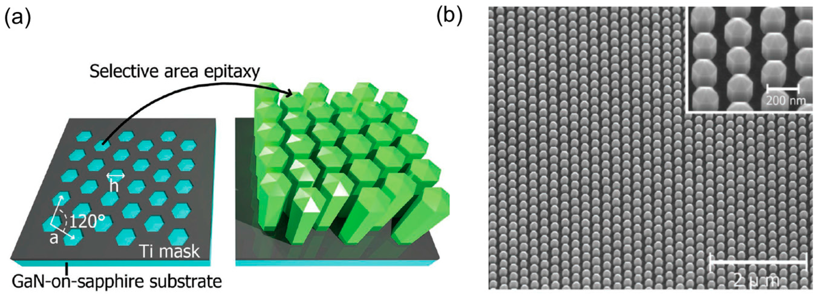
The first approach is the most common one, which occurs on patterned substrates. In this approach, a mask layer, e.g., SiOx, SiNx, or Ti, is first deposited on substrates such as a Si or GaN template, followed by e-beam lithography to create nano-sized openings, as illustrated in Figure 1a [55]. Due to different atom kinetics on the surface of the mask layer and substrate, the nucleation process takes place preferentially in the openings [55,56,57,58,59,60,61,62,63,64,65,66]. Figure 1b shows a scanning electron microscopy (SEM) image of GaN nanowires grown by selective area epitaxy [55]. It is seen that nanowires with the same height, diameter, and spacing are grown. The second approach utilizes regular nanowire arrays as the template. Due to shadow effects of adjacent nanowires, the growth of desired nanowires takes place on such nanowire templates. Using this approach, Yamano et al. demonstrated Al(Ga)N nanowires on the top-down etched GaN nanopillars on GaN template [67].
Besides the excellent control of the nanowire formation site and size uniformity, using selective area epitaxy can lead to nearly defect-free, quasi-epilayer template with arbitrary alloy composition, through a controlled coalescence process. For example, AlGaN quasi-epilayer templates have been obtained through coalescing AlGaN nanowires grown by selective area epitaxy on Ti-patterned GaN template [55]. This could open up an important approach to grow nearly defect-free III-nitride device layers on lattice matched template.
3. Mg-Doped InN Nanowires
Mg-doped InN nanowires have been investigated previously [68,69]. Nevertheless, these Mg-doped InN nanowires have remained n-type. Recently, with an improved MBE growth process and a careful tuning of the growth parameters of Mg-doped InN nanowires on Si substrate, direct evidence for p-type doping, including a direct measurement of p-type conduction [43], and electroluminescence from InN p-i-n photodiodes [70], has been provided. In this section, these recent progresses are discussed.
3.1. Mg-Dopant Incorporation
Prior to nanowire growth, a thin In seeding layer is deposited. At elevated growth temperatures, the In seeding layer turns into In droplets, which can enhance the formation of Mg-doped InN nanowires. The typical growth parameters include a nitrogen flow rate of 1 sccm, a nitrogen plasma power of 350 W, an In flux of 6 × 10⁻⁸ Torr, and a substrate temperature of 480 °C. Mg fluxes are in the range of ~1 × 10⁻¹¹ to 3 × 10⁻¹⁰ Torr [43,71].
Figure 2a shows the SEM image of Mg-doped InN nanowires. It is seen that hexagonal-shaped nanowires are formed. Figure 2b shows a high-resolution transmission electron microscopy (TEM) image taken from the root region of a single nanowire. The crystalline plane can be clearly observed. The growth direction is along c-axis, marked by the arrow. Detailed high-resolution TEM studies further suggest that such nanowires are free of stacking faults and misfit dislocations [43,71].
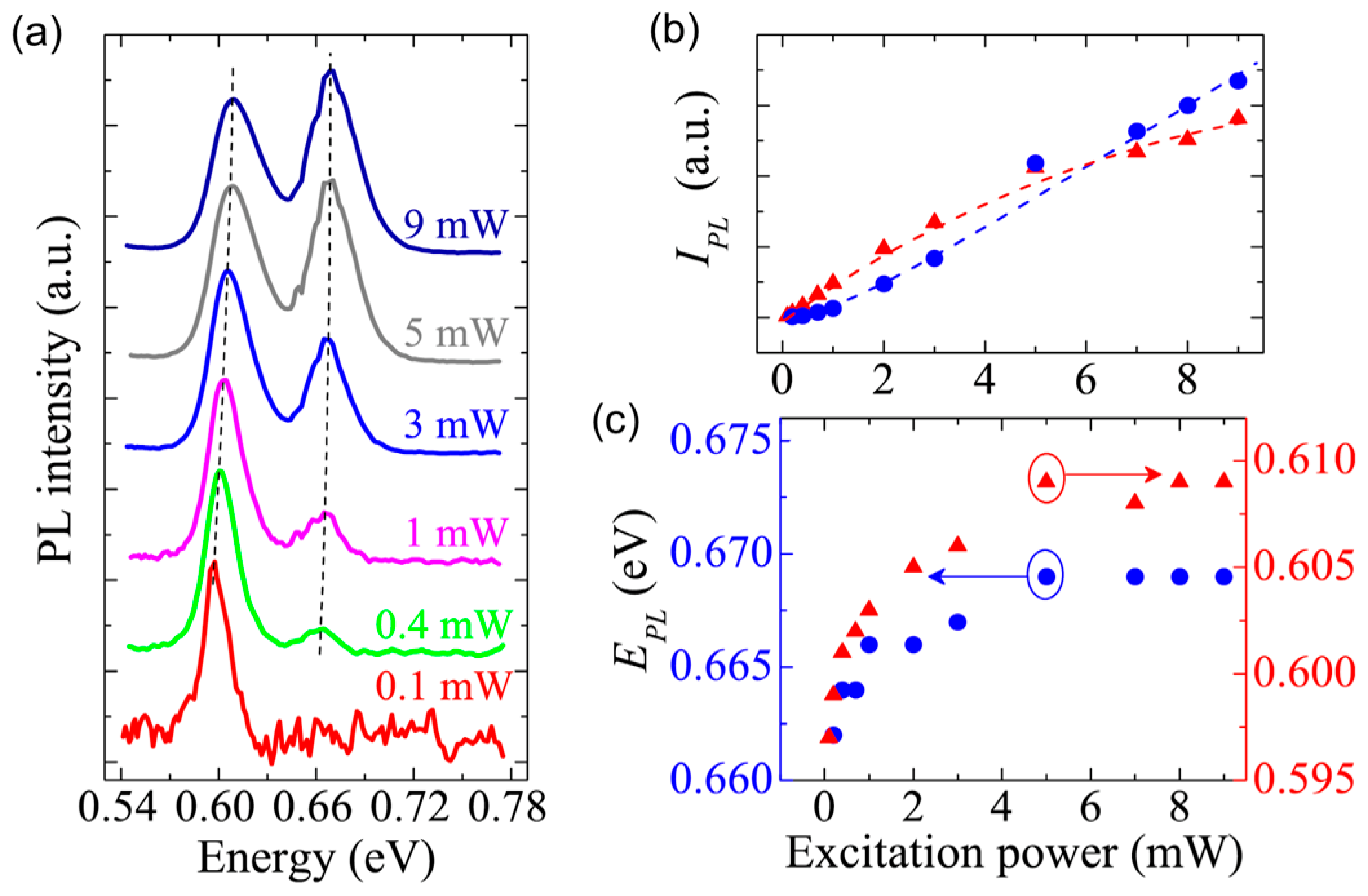
The incorporation of Mg dopants is confirmed by photoluminescence experiments. Figure 3a shows the power-dependent photoluminescence spectra measured from Mg-doped InN nanowires with a Mg cell temperature of 190 °C (Mg flux is around 1 × 10⁻¹¹ Torr) [71]. It is seen that besides the near band edge emission peak around 0.67 eV, another low-energy peak around 0.61 eV is measured (e.g., under an excitation power of 9 mW). The energy separation is about 60 meV, which is consistent with the Mg activation energy in InN, indicating that the low-energy peak is due to the Mg-acceptor related radiative recombination. In addition, as the excitation power reduces, the low-energy peak gradually dominates the emission spectra; and under the lowest excitation power (0.1 mW) only the low-energy peak is measured. This further confirms that the nature of the low-energy peak is an acceptor related recombination.
The excitation power dependent integrated intensity (IPL) and peak energy (EPL) are further extracted. The superscripts L and H denote the low-energy peak and high-energy peak, respectively. As illustrated in Figure 3b, both IPLL (in red triangles) and IPLH (in blue circles) increase as the excitation power increases. However, IPLL increases faster at low excitations, followed by a saturation trend at high excitations. This is in contrast to IPLH, which rises slower at low excitations and faster at high excitations, with no sign of saturation. This difference is attributed to the redistribution of hole population in the Mg-acceptor energy levels and valence band [71,72]. Moreover, as illustrated in Figure 3c, at low excitations both EPLL (in red triangles) and EPLH (in blue circles) exhibit a blue-shift of 12 meV and 7 meV, respectively, and then stay nearly constant at high excitations. Detailed analysis indicates that the low-energy peak and high-energy peak are due to neutral donor-acceptor pair recombination (D0A0) and recombination associated with valence band tail, respectively [71].
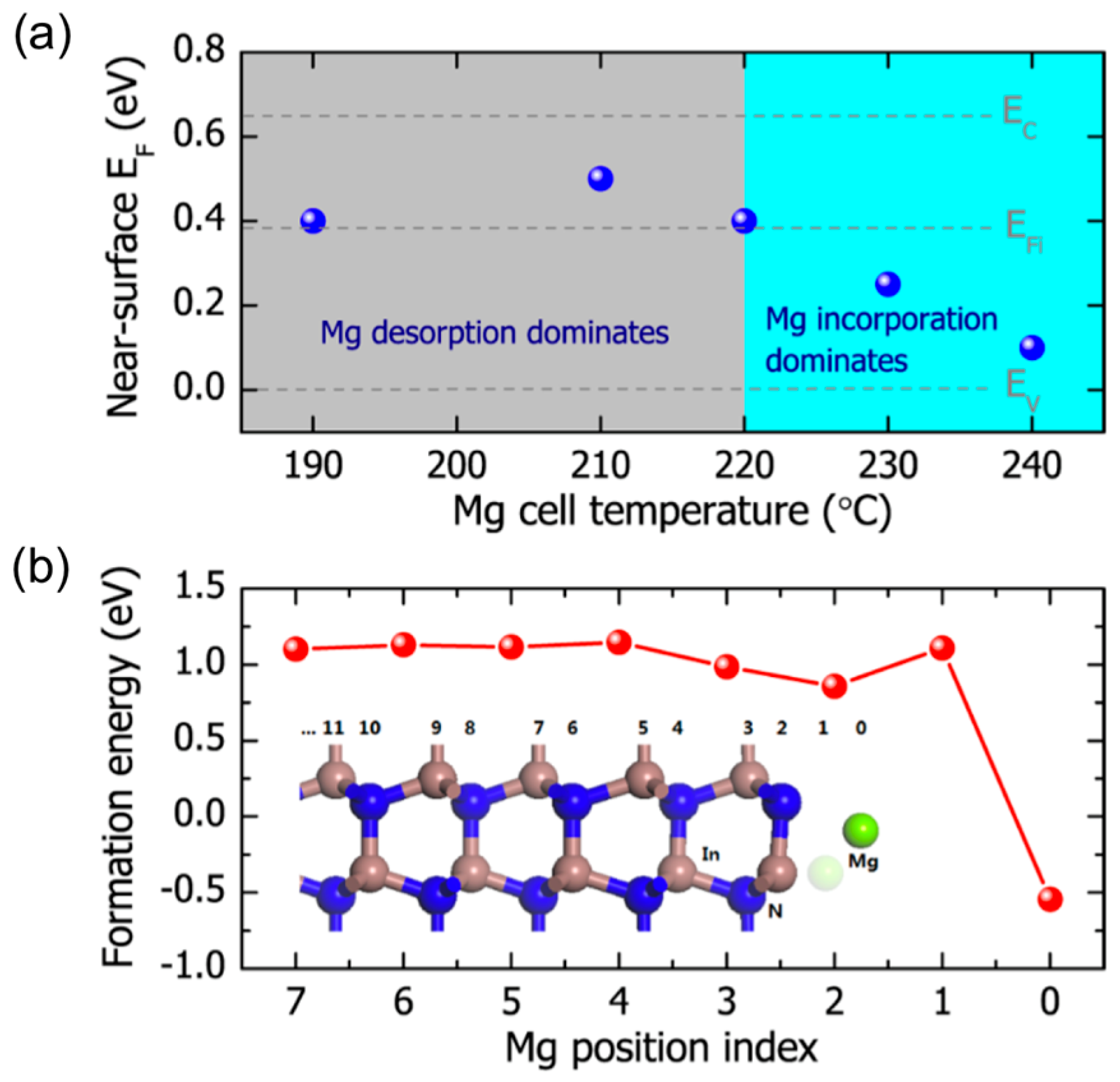
The near-surface Fermi-level of Mg-doped InN nanowire samples with different doping levels is measured by X-ray photoelectron spectroscopy (XPS) [43]. The signal is collected from nanowire sidewalls on as-grown nanowire ensembles. Moreover, the scans are also compared to Si substrate background signals, to exclude artifacts. Statistically, a variation of the near-surface Fermi-level is measured as the Mg cell temperature changes from 190 to 240 °C (Mg flux varies from ~1 × 10⁻¹¹ to 3 × 10⁻¹⁰ Torr). As illustrated in Figure 4a, for low Mg-doped samples the near-surface Fermi-level is similar to what is measured in nearly intrinsic InN nanowires, i.e., ~0.4–0.5 eV above the valence band maximum; and for the sample with the highest Mg doping it is reduced to ~0.1 eV above the valence band maximum. These results indicate that with Mg doping the near-surface region can be converted to p-type, which is in clear contrast to the previously reported Mg-doped InN epilayers, wherein the surface electron accumulation and Fermi-level pinning in the conduction band are commonly observed [19,21,24,25].
To understand the Mg incorporation into InN nanowires, first principle calculations have been performed [43]. As shown from Figure 4b, the Mg formation energy is noticeably lower at the surface compared to that in the bulk. The reduction of Mg formation energy can therefore enhance Mg-dopant incorporation. Such an effect is attributed to the reduced lattice strain imposed by surface dopants compared to bulk dopants. A similar effect has also been measured in other semiconductor nanowires [42,45,46,47,73]. The Mg incorporation into InN nanowires thus can be understood through two competing processes: (a) Mg surface desorption at elevated growth temperatures; and (b) enhanced Mg incorporation, due to the lowering of Mg formation energy. These two factors together can largely explain the Mg-doping concentration dependent near-surface Fermi-level in Mg-doped InN nanowires [43].
3.2. Direct Evidence for p-Type Doping
3.2.1. A Direct Measurement of p-Type Conduction
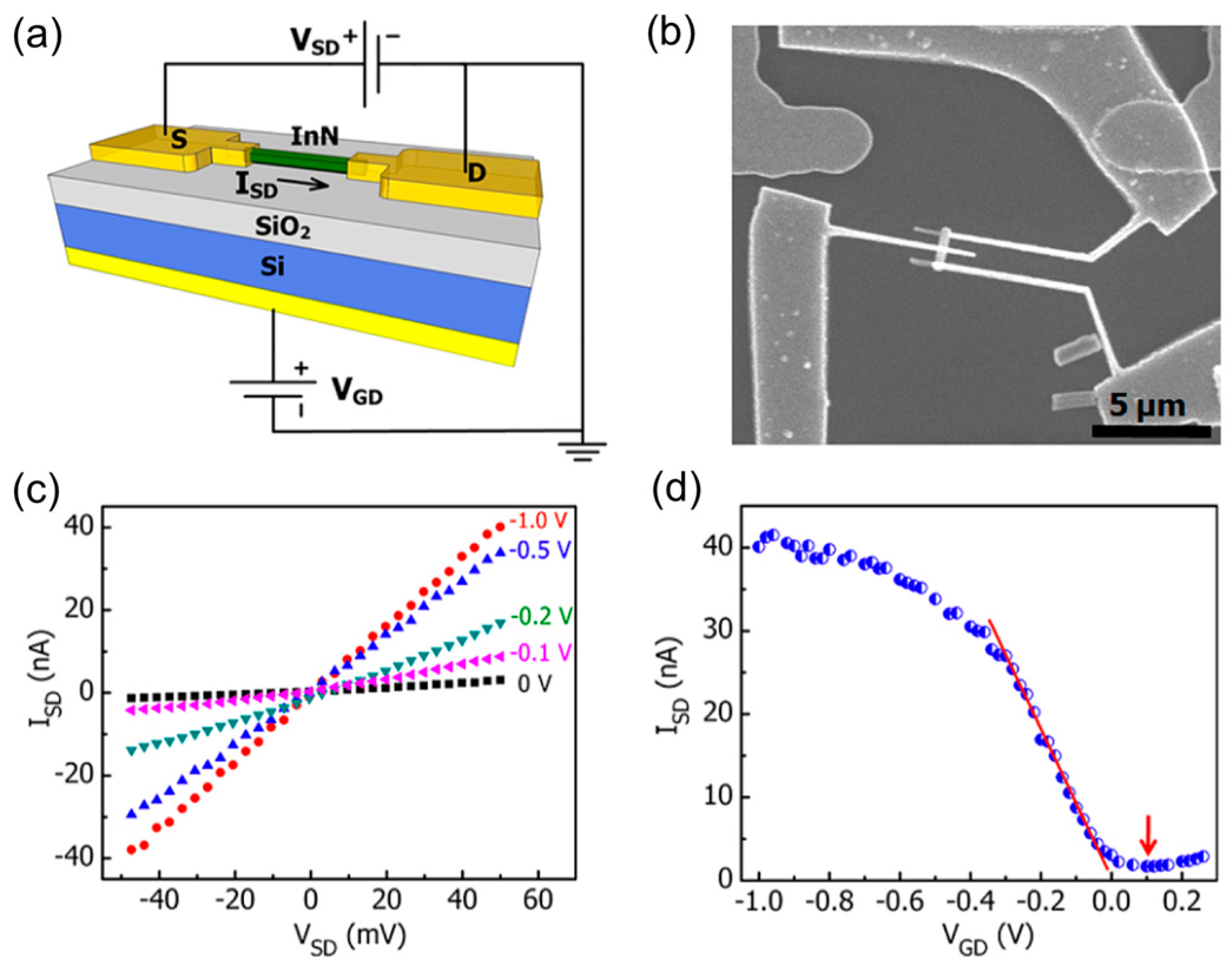
p-Type conduction is directly measured from single Mg-doped InN nanowires with a back-gate field-effect transistor configuration [43,74]. The device schematic is shown in Figure 5a. The corresponding SEM image is shown in Figure 5b. The source-drain current (ISD) vs. the source-drain voltage (VSD) under different back-gate voltages (VGD) is shown in Figure 5c. It is seen that the channel conduction (ISD/VSD) increases as a more negative VGD is applied. This increase in channel conduction with increasingly negative back-gate voltage provides unambiguous evidence for p-type conduction. In addition, the conduction minimum occurs at a slightly positive VGD (marked by the arrow in Figure 5d), indicating a p-type conduction at zero back-gate voltage. The field-effect hole mobility is further derived to be 100 cm2/Vs from transfer characteristics (ISD–VGD dependence), which agrees very well with the ensemble Monte Carlo calculation [75]. With this hole mobility, the hole concentration (at VGD = 0 V) is further estimated to be 5 × 1015 cm−3.
3.2.2. Electroluminescence from InN p-i-n Photodiode
Direct evidence for p-type doping into InN is further provided by the measurement of electroluminescence from InN p-i-n photodiodes [70]. Schematic of a single InN nanowire p-i-n LED is shown in Figure 6a. The electrical injection is realized from two metal contacts, which are fabricated through standard e-beam lithography and metallization processes. An SEM image of a fabricated device is shown in Figure 6b.
The I-V characteristics in a semi-log scale are shown in Figure 6c. The large reverse bias current is mainly due to the presence of current leakage channel [70]. Shown in the inset of Figure 6d is the electroluminescence spectrum measured under an injection current of 0.5 mA. An emission peak around 0.71 eV is clearly measured, which corresponds to a wavelength of 1.75 μm. The integrated intensity vs. injection current is shown in Figure 6d. It is seen that the light intensity increases linearly with the increase of injection current.
There are a couple of factors that lead to the realization of p-type InN using nanowire structures:
- Due to efficient strain relaxation in nanowires, the density of defects (e.g., stacking faults, misfit dislocations) is drastically reduced. Moreover, the formation of nitrogen-vacancy related defect donors can be suppressed, due to the use of nitrogen-rich conditions.
- The In-substitutional Mg formation energy is reduced in InN nanowires, which can enhance Mg incorporation.
- Previous studies on the correlated surface charge properties and morphology of InN nanowires indicate that InN nanowires with tapered morphology tend to have high background electron concentration and surface electron accumulation, due to surface defects [44,76,77]. In this regard, maintaining excellent hexagonal-shaped morphology is another important factor to realize p-type InN nanowires.
4. Mg-Doped AlN Nanowires and Their Applications in Deep UV Optoelectronics
Previously, Mg-doped AlN nanowires synthesized by chemical vapor deposition (CVD) and arc discharging have been reported [78,79,80,81,82]. The properties of these Mg-doped AlN nanowires, however, are largely determined by various defect energy levels in the ultra-wide-bandgap AlN, e.g., only defect-related optical emission can be measured [78]. Recently, with the use of MBE, Mg-doped AlN nanowires with excellent optical and electrical properties are obtained [42,83,84,85,86], which represents a critical step towards AlN nanowire-based deep UV optoelectronic devices. In this section, we discuss recent progress made on Mg-doped AlN nanowires grown by MBE, and their applications to deep UV LEDs and lasers.
4.1. Mg-Dopant Incorporation and p-Type Conduction
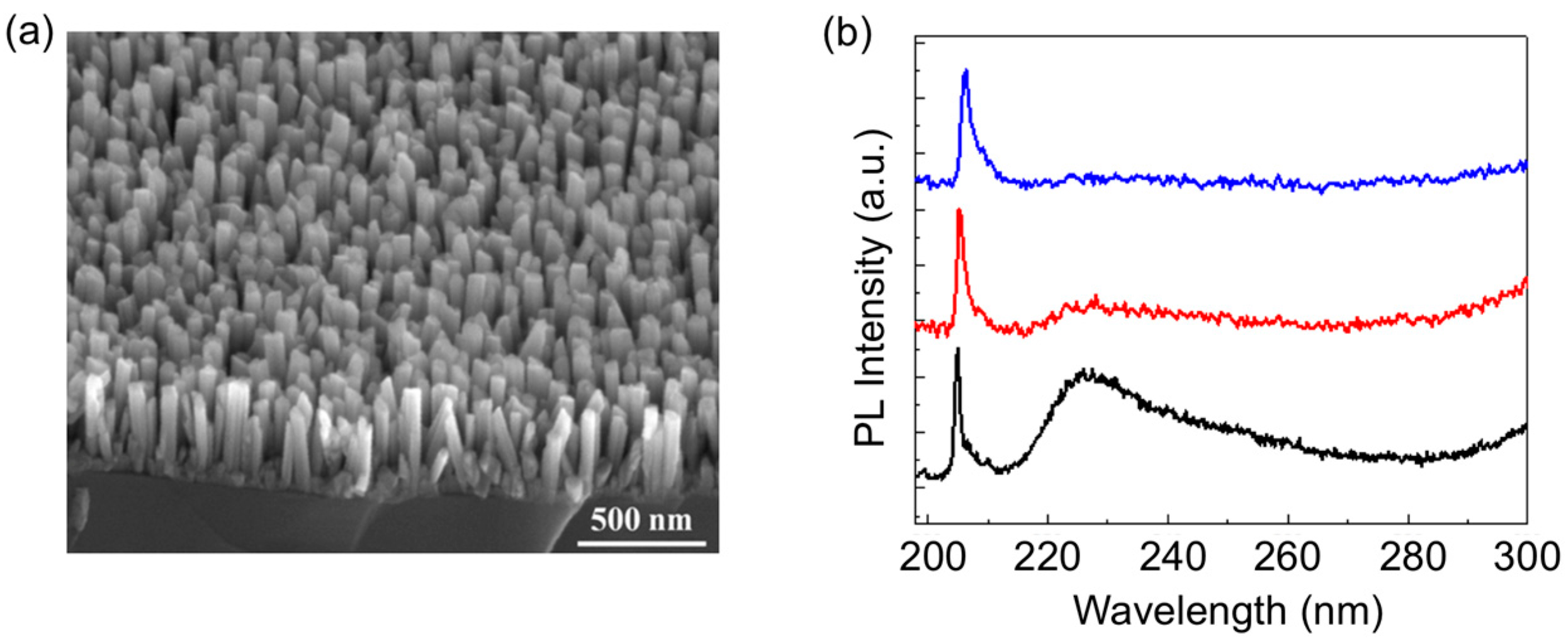
To promote nanowire formation, a spontaneously formed GaN nanowire template is grown first [42,84,85,86]. Detailed studies further indicate that the growth condition of such GaN nanowire templates plays an important role on the formation of the AlN nanowire segment on top [42,53,84,85]. Moreover, to reduce Mg surface desorption, a relatively low substrate temperature is used. The typical growth condition includes a nitrogen flow rate of 1 sccm, a nitrogen plasma power of 350 W, and a substrate temperature of 800 °C. Al and Mg fluxes are in the range of 2–6 × 10⁻⁸ Torr and 3 × 10⁻⁹ to 9 × 10⁻⁸ Torr, respectively [42,84,85]. Under optimized growth conditions, relatively uniform Mg-doped AlN nanowires can be obtained, as shown in Figure 7a. Photoluminescence spectra measured from Mg-doped AlN nanowire samples with different doping concentrations are shown in Figure 7b. It is seen that as Mg-doping concentration increases (from the top spectrum to the bottom spectrum), another low-energy peak, which is separated from the band edge emission peak by 0.5 eV, is measured. This energy separation is consistent with the Mg activation energy in AlN [39], confirming the incorporation of Mg dopants into AlN nanowires.
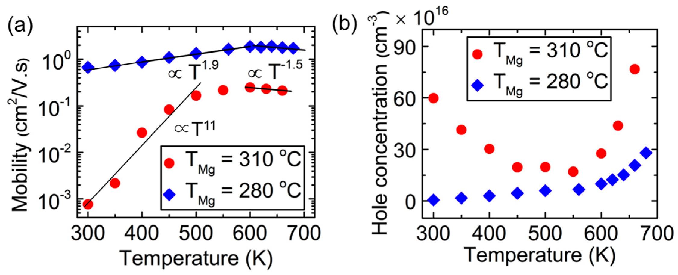
The electrical transport properties of Mg-doped AlN nanowires have also been investigated by back-gate field-effect transistor configuration [87], as shown in Figure 8a. An SEM image of a fabricated single nanowire device is shown in Figure 8b. VGD dependent ISD vs. VSD is shown in Figure 8c. It is seen that ISD/VSD exhibits a clear increase as a more negative VGD is applied, suggesting a p-type conduction. The transfer characteristics at VSD = 0.2 V are shown in Figure 8d. It is seen that ISD reaches a minimum at VGD = 0.2 V, indicating a p-type conduction at VGD = 0 V.
By further analyzing transfer characteristics, field-effect hole mobility can be derived [87]. Shown by the blue squares in Figure 9a (in conjunction with Figure 8d), at room temperature hole mobility is 0.67 cm2/Vs, corresponding to a free hole concentration of 5 × 1015 cm−3 (illustrated by blue squares in Figure 9b). With the increase of Mg-doping concentration, the room-temperature hole mobility is reduced to 7.7 × 10⁻⁴ cm2/Vs (illustrated by red circles in Figure 9a), corresponding to a free hole concentration of 6 × 1017 cm−3 (illustrated by red circles in Figure 9b). These free hole concentrations are considerably higher compared to the previously reported values from Mg-doped AlN epilayers grown by MOCVD (on the order of 1010 cm−3) [39]. The temperature dependent hole mobility and hole concentration can be explained by conduction occurring in both valence band and Mg-impurity band [87]. Similar temperature dependence has also been previously measured in GaN [88].
There are two important factors that contribute to such unusually high free hole concentration/efficient p-type conduction in the ultra-wide-bandgap AlN:
- AlN nanowires possess drastically reduced defect density. This is, first of all, due to efficient strain relaxation in nanowires. On top of this, other impurities, such as carbon, can be further minimized with the use of plasma-assisted MBE, compared to CVD or MOCVD. Additionally, such nanowires are formed under nitrogen-rich conditions, wherein nitrogen-vacancy related defects (donors) can be minimized.
- Similar to Mg doping in InN nanowires, the Al-substitutional Mg formation energy is also drastically reduced in AlN nanowires, thereby leading to significantly enhanced Mg-dopant incorporation [42]. This could lead to two mechanisms that enhance p-type conduction. Firstly, the formation of the Mg-impurity band enables the impurity band conduction, which requires much less activation energy for conduction compared to the energy needed to generate a valence band hole. Secondly, due to the band tailing effect and broadened Mg energy levels associated with the enhanced Mg-dopant incorporation, a portion of Mg dopants could have reduced activation energy, which further improves p-type conduction in the valence band.
4.2. AlN Nanowire-Based Deep UV Optoelectronic Devices
The large operation voltage of AlGaN quantum well deep UV LEDs [5,7,10], and moreover, the difficulty to obtain lasing shorter than 336 nm through direct electrical injection with AlGaN quantum wells [6], are partially attributed to poor p-type doping in Al-rich AlGaN alloys. As shown above, with the MBE-grown nanowire structures, Mg dopants can be efficiently incorporated; and free hole concentrations up to 6 × 1017 cm−3 have been derived in AlN nanowires, which are orders of magnitude higher compared to the previously reported p-type AlN epilayers grown by MOCVD [39]. This essentially removes the p-type doping challenge in Al-rich AlGaN alloys, and represents an important step towards electrically-injected AlGaN deep UV lasers and deep UV LEDs with high electrical efficiency. In this section, we discuss the first AlN nanowire LEDs and lasing through direct electrical injection with AlGaN nanowires in the deep UV band.
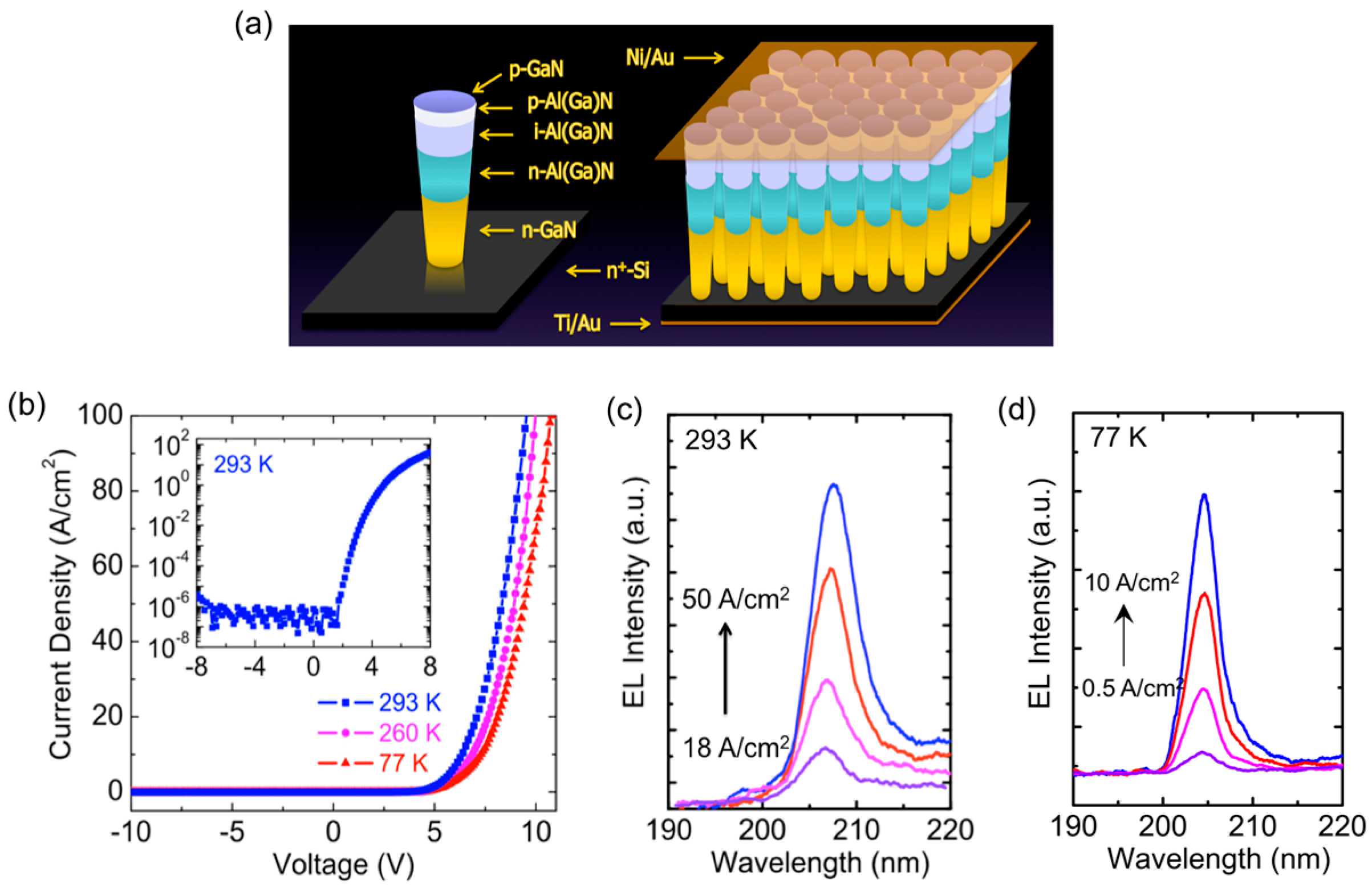
4.2.1. AlN Nanowire LEDs
The device structure consists of n-GaN, AlN p-i-n homojunction, and p-AlGaN contact layer [42,84], as illustrated in Figure 10a. Figure 10b shows the I-V characteristics of AlN nanowire LEDs measured at different temperatures, with the inset showing the room-temperature I-V characteristics in a semi-log scale. The turn on voltage is around 5.5 V, which is consistent with the bandgap energy of AlN. Moreover, at 20 A/cm2, the forward voltage is only 7 V, which corresponds to an electrical efficiency of 86% for a photon energy of 6 eV. This electrical performance is drastically improved compared to the previously reported planar AlN LEDs [39], which is attributed to the significantly enhanced Mg-dopant incorporation in nanowire structures and the resultant efficient p-type conduction, as discussed previously. Recently, AlGaN ternary nanowire deep UV LEDs with excellent electrical performance have also been demonstrated [42,89,90,91].
Electroluminescence is measured at both room and low temperatures, as shown in Figure 10c,d, respectively. The spectra are collected by an optical fiber from the device top. Compared to emission peak around 207 nm at room temperature, the emission peak at low temperature is blue-shifted to 204 nm, due to the increase of bandgap energy. A negligible shift of the emission peak wavelength is found in both temperatures, consistent with exciton emission.
4.2.2. Electrically-Injected Deep UV Lasers
By exploiting the light localization effect in randomly arranged AlGaN nanowires, lasing phenomenon by direct electrical injection has been demonstrated for the first time in the deep UV bands [50,92,93,94]. The layer-by-layer structure in each individual nanowire is shown in Figure 11a, which consists of the n-GaN contact layer, n-AlGaN cladding layer, AlGaN active region, p-AlGaN cladding layer, and p-GaN contact layer. Shown in Figure 11b is the simulated in-plane electrical field distribution for a TM polarized light at 240 nm using the RF module of Comsol Multiphysics 4.3b. It is seen that strong light confinement can be realized [94]. On the other hand, the optical confinement in the vertical direction is realized through the effective refractive index variation along the nanowire growth direction (c-axis). Due to the inversely tapered morphology, the effective index is larger near the nanowire top, which gives light confinement, as illustrated in Figure 11c.
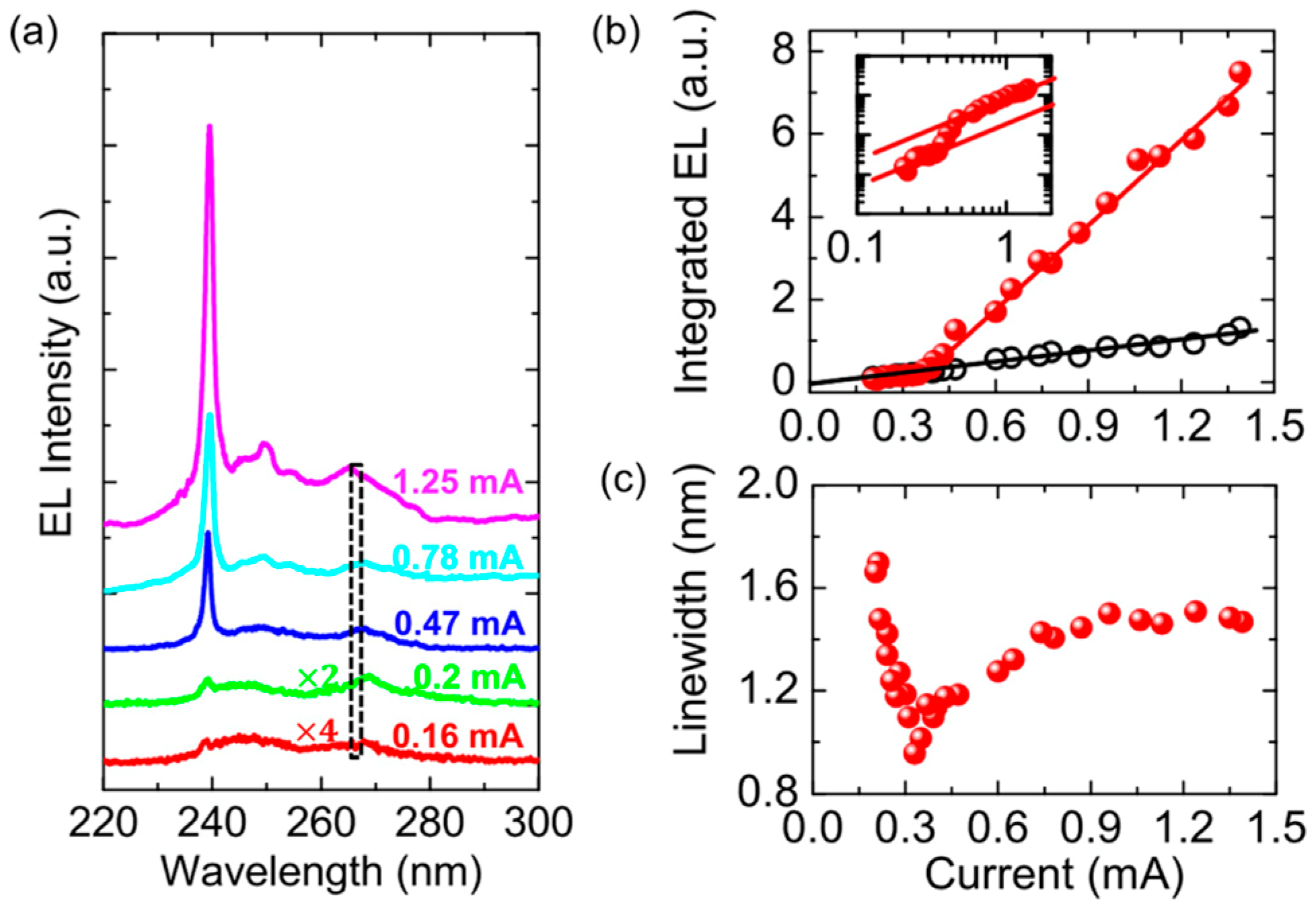
Electrically-injected devices are fabricated using standard photolithography and metallization techniques. The light emission is collected by a deep UV objective from the device top surface, spectrally resolved by a high-resolution spectrometer, and detected by a charge-coupled device (CCD) camera. Figure 12a illustrates lasing at 239 nm: under a low injection current, only a very broad emission spectrum is measured. With the increase of injection current, a sharp peak centered at 239 nm appears. The light intensity vs. injection current is shown in Figure 12b, which exhibits a distinct lasing threshold at 0.35 mA. Shown by the inset of Figure 12b, the s-shaped light intensity vs. injection current in the logarithmic scale further confirms the lasing. Figure 12c shows the linewidth reduction from 1.7 nm to 0.9 nm near the threshold. A non-lasing cavity mode around 267 nm is also analyzed. Shown by the open black circles in Figure 12b, the intensity stays nearly constant above the threshold, further supporting the lasing at 239 nm.
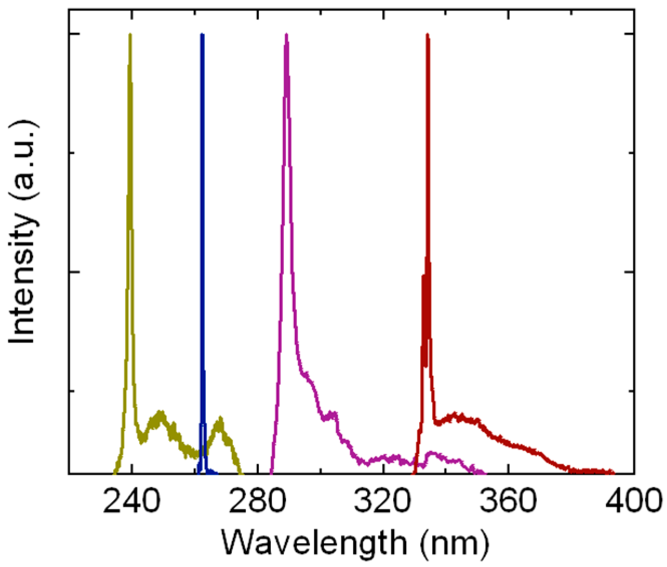
With changing cavity design and alloy composition, lasing at different wavelengths can be obtained, as shown in Figure 13. The observation of lasing with AlGaN nanowires through electrical injection is attributed to a few key elements: (a) nanowires with much reduced defect density; (b) efficient p-type doping in nanowire structures; (c) quantum confinement of charge carriers due to the formation of atomic-/nano-scale AlGaN clusters; (d) surface passivation by Al-rich AlGaN shell, and (e) high Q optical cavity.
5. Conclusions and Future Prospects
In this article, we review recent advances on Mg-doped InN and AlN nanowire structures grown by MBE, including direct evidence for p-type doping in Mg-doped InN nanowires and high free hole concentrations in Mg-doped AlN nanowires. These achievements in p-type doping are attributed to the much reduced defect density and enhanced Mg-dopant incorporation in nanowires, as well as the negligible level of impurity incorporation with the use of plasma-assisted MBE. With addressing these enduring p-type doping challenges, devices that were not possible previously are demonstrated, such as InN p-i-n LEDs and electrically-injected AlGaN deep UV lasers.
The p-type InN and AlN nanowires discussed so far are formed on Si substrate. In fact, a number of recent studies indicate that the MBE-grown III-nitride nanowires could be substrate independent [95,96,97,98,99], i.e., the MBE-grown III-nitride nanowires can be essentially formed on any substrate. For example, GaN, InGaN/GaN dot-in-a-wire, and InN nanowire structures have been demonstrated on silicon oxide [95,99,100,101]. Moreover, their optical qualities seem to be not compromised, e.g., InN and GaN nanowires grown on silicon oxide show similar photoluminescence characteristics compared to the nanowires grown on Si [99]. Recently, visible and UV LEDs with InGaN and AlGaN quantum wells/quantum disks have been demonstrated on metal substrates [102,103,104,105,106]. III-nitride nanowire structures on graphene have also been investigated. These non-conventional MBE-grown III-nitride nanostructures could not only provide versatile playgrounds to study the fundamentals of MBE growth, but also open up new avenues for device applications, including infrared, deep visible, and deep UV LEDs and lasers, as well as solar fuel devices and systems. Further combining with the improved scale-up capability of MBE reactors today, it is thus believed that MBE, together with III-nitride nanostructures, could be a game-changer for a number of optoelectronic devices in the future.
Acknowledgments
This work is supported by National Research Council Canada and US Army Research Office.
Author Contributions
Songrui Zhao wrote the paper. Zetian Mi made comments and revision.
Conflicts of Interest
The authors declare no conflict of interest. The founding sponsors had no role in the design of the study; in the collection, analyses, or interpretation of data; in the writing of the manuscript, and in the decision to publish the results.
References
- Wu, J. When group-III nitrides go infrared: New properties and perspectives. J. Appl. Phys. 2009, 106, 011101. [Google Scholar] [CrossRef]
- Nakamura, S.; Pearton, S.; Fasol, G. The blue laser diode: The complete story. In Science & Business Media; Springer: Berlin/Heidelberg, Germany, 2013. [Google Scholar]
- Akasaki, I. Key inventions in the history of nitride-based blue LED and LD. J. Cryst. Growth 2007, 300, 2–10. [Google Scholar] [CrossRef]
- Yoshikawa, A.; Wang, X.; Ishitani, Y.; Uedono, A. Recent advances and challenges for successful p-type control of InN films with Mg acceptor doping by molecular beam epitaxy. Phys. Status Solidi A 2010, 207, 1011–1023. [Google Scholar] [CrossRef]
- Khan, A.; Balakrishnan, K.; Katona, T. Ultraviolet light-emitting diodes based on group three nitrides. Nat. Photonics 2008, 2, 77–84. [Google Scholar] [CrossRef]
- Yoshida, H.; Kuwabara, M.; Yamashita, Y.; Uchiyama, K.; Kan, H. The current status of ultraviolet laser diodes. Phys. Status Solidi A 2011, 208, 1586–1589. [Google Scholar] [CrossRef]
- Kneissl, M.; Kolbe, T.; Chua, C.; Kueller, V.; Lobo, N.; Stellmach, J.; Knauer, A.; Rodriguez, H.; Einfeldt, S.; Yang, Z.; et al. Advances in group III-nitride-based deep UV light-emitting diode technology. Semicond. Sci. Technol. 2011, 26, 014036. [Google Scholar] [CrossRef]
- Yamamoto, A.; Islam, M.R.; Kang, T.-T.; Hashimoto, A. Recent advances in InN-based solar cells: Status and challenges in InGaN and InGaN solar cells. Phys. Status Solidi C 2010, 7, 1309–1316. [Google Scholar] [CrossRef]
- Bhuiyan, A.G.; Sugita, K.; Hashimoto, A.; Yamamoto, A. InGaN solar cells: Present state of the art and important challenges. IEEE J. Photovotaics 2012, 2, 276–293. [Google Scholar] [CrossRef]
- Hirayama, H.; Maeda, N.; Fujikawa, S.; Toyoda, S.; Kamata, N. Recent progress and future prospects of AlGaN-based high-efficiency deep-ultraviolet light-emitting diodes. Jpn. J. Appl. Phys. 2014, 53, 100209. [Google Scholar] [CrossRef]
- Van de Walle, C.G.; Neugebauer, J. Universal alignment of hydrogen levels in semiconductors, insulators and solutions. Nature 2003, 423, 626. [Google Scholar] [CrossRef] [PubMed]
- Wang, X.; Liu, S.; Ma, N.; Feng, L.; Chen, G.; Xu, F.; Tang, N.; Huang, S.; Chen, K.J.; Zhou, S.; et al. High-electron-mobility InN layers grown by boundary-temperature-controlled epitaxy. Appl. Phys. Express 2012, 5, 015502. [Google Scholar] [CrossRef]
- Fehlberg, T.B.; Umana-Membreno, G.A.; Gallinat, C.S.; Koblmüller, G.; Bernardis, S.; Nener, B.D.; Parish, G.; Speck, J.S. Characterisation of multiple carrier transport in indium nitride grown by molecular beam epitaxy. Phys. Status Solidi C 2007, 4, 2423–2427. [Google Scholar] [CrossRef]
- Wang, K.; Araki, T.; Yu, K.M.; Katsuki, T.; Mayer, M.A.; Alarcon-Llado, E.; Ager, J.W.; Walukiewicz, W.; Nanishi, Y. P-type InGaN across the entire alloy composition range. Appl. Phys. Lett. 2013, 102, 102111. [Google Scholar] [CrossRef]
- Ruffenach, S.; Moret, M.; Briot, O.; Gil, B. Recent advances in the MOVPE growth of indium nitride. Phys. Status Solidi A 2010, 207, 9–18. [Google Scholar] [CrossRef]
- Zhao, S.; Mi, Z. Chapter Eight-InN Nanowires: Epitaxial Growth, Characterization, and Device Applications. Semicond. Semimet. 2017, 96, 267–304. [Google Scholar]
- Calarco, R. InN nanowires: Growth and optoelectronic properties. Materials 2012, 5, 2137. [Google Scholar] [CrossRef]
- Van de Walle, C.G.; Lyons, J.L.; Janotti, A. Controlling the conductivity of InN. Phys. Status Solidi A 2010, 207, 1024–1036. [Google Scholar] [CrossRef]
- Anderson, P.A.; Swartz, C.H.; Carder, D.; Reeves, R.J.; Durbin, S.M.; Chandril, S.; Myers, T.H. Buried p-type layers in Mg-doped InN. Appl. Phys. Lett. 2006, 89, 184104. [Google Scholar] [CrossRef]
- Mayer, M.A.; Choi, S.; Bierwagen, O.; Smith, H.M.; Haller, E.E.; Speck, J.S.; Walukiewicz, W. Electrical and optical properties of p-type InN. J. Appl. Phys. 2011, 110, 123707. [Google Scholar] [CrossRef]
- Wang, X.; Che, S.-B.; Ishitani, Y.; Yoshikawa, A. Growth and properties of Mg-doped In-polar InN films. Appl. Phys. Lett. 2007, 90, 201913. [Google Scholar] [CrossRef]
- Khan, N.; Nepal, N.; Sedhain, A.; Lin, J.Y.; Jiang, H.X. Mg acceptor level in InN epilayers probed by photoluminescence. Appl. Phys. Lett. 2007, 91, 012101. [Google Scholar] [CrossRef]
- Wang, X.; Che, S.-B.; Ishitani, Y.; Yoshikawa, A. Hole mobility in Mg-doped p-type InN films. Appl. Phys. Lett. 2008, 92, 132108. [Google Scholar] [CrossRef]
- Wang, K.; Miller, N.; Iwamoto, R.; Yamaguchi, T.; Mayer, M.A.; Araki, T.; Nanishi, Y.; Yu, K.M.; Haller, E.E.; Walukiewicz, W.; et al. Mg doped InN and confirmation of free holes in InN. Appl. Phys. Lett. 2011, 98, 042104. [Google Scholar] [CrossRef]
- Ager, J.W.; Miller, N.; Jones, R.E.; Yu, K.M.; Wu, J.; Schaff, W.J.; Walukiewicz, W. Mg-doped InN and InGaN—Photoluminescence, capacitance–voltage and thermopower measurements. Phys. Status Solidi B 2008, 245, 873–877. [Google Scholar] [CrossRef]
- Wang, X.; Che, S.-B.; Ishitani, Y.; Yoshikawa, A. Systematic study on p-type doping control of InN with different Mg concentrations in both In and N polarities. Appl. Phys. Lett. 2007, 91, 242111. [Google Scholar] [CrossRef]
- Dmowski, L.H.; Baj, M.; Suski, T.; Przybytek, J.; Czernecki, R.; Wang, X.; Yoshikawa, A.; Lu, H.; Schaff, W.J.; Muto, D.; et al. Search for free holes in InN:Mg-interplay between surface layer and Mg-acceptor doped interior. J. Appl. Phys. 2009, 105, 123713. [Google Scholar] [CrossRef]
- Dmowski, L.H.; Baj, M.; Konczewicz, L.; Suski, T.; Maude, D.K.; Grzanka, S.; Wang, X.Q.; Yoshikawa, A. Coexistence of free holes and electrons in InN:Mg with In- and N-growth polarities. J. Appl. Phys. 2012, 111, 093719. [Google Scholar] [CrossRef]
- Li, S.; Zhang, T.; Wu, J.; Yang, Y.; Wang, Z.; Wu, Z.; Chen, Z.; Jiang, Y. Polarization induced hole doping in graded AlxGa1−xN (x = 0.7~1) layer grown by molecular beam epitaxy. Appl. Phys. Lett. 2013, 102, 062108. [Google Scholar] [CrossRef]
- Kinoshita, T.; Obata, T.; Yanagi, H.; Inoue, S.-I. High p-type conduction in high-Al content Mg-doped AlGaN. Appl. Phys. Lett. 2013, 102, 012105. [Google Scholar] [CrossRef]
- Nakarmi, M.L.; Nepal, N.; Ugolini, C.; Altahtamouni, T.M.; Lin, J.Y.; Jiang, H.X. Correlation between optical and electrical properties of Mg-doped AlGaN epilayers. Appl. Phys. Lett. 2006, 89, 152120. [Google Scholar] [CrossRef]
- Allerman, A.A.; Crawford, M.H.; Miller, M.A.; Lee, S.R. Growth and characterization of Mg-doped AlGaN–AlN short-period superlattices for deep-UV optoelectronic devices. J. Cryst. Growth 2010, 312, 756–761. [Google Scholar] [CrossRef]
- Waldron, E.L.; Graff, J.W.; Schubert, E.F. Improved mobilities and resistivities in modulation-doped p-type AlGaN/GaN superlattices. Appl. Phys. Lett. 2001, 79, 2737. [Google Scholar] [CrossRef]
- Liao, Y.; Kao, C.-K.; Thomidis, C.; Moldawer, A.; Woodward, J.; Bhattarai, D.; Moustakas, T.D. Recent progress of efficient deep UV-LEDs by plasma-assisted molecular beam epitaxy. Phys. Status Solidi C 2012, 9, 798–801. [Google Scholar] [CrossRef]
- Zhang, Y.; Krishnamoorthy, S.; Johnson, J.M.; Akyol, F.; Allerman, A.; Moseley, M.W.; Armstrong, A.; Hwang, J.; Rajan, S. Interband tunneling for hole injection in III-nitride ultraviolet emitters. Appl. Phys. Lett. 2015, 106, 141103. [Google Scholar] [CrossRef]
- Zhao, S.; Mi, Z. Al (Ga) N Nanowire Deep Ultraviolet Optoelectronics. Semicond. Semimet. 2017, 96, 167–199. [Google Scholar]
- Nakarmi, M.L.; Kim, K.H.; Khizar, M.; Fan, Z.Y.; Lin, J.Y.; Jiang, H.X. Electrical and optical properties of Mg-doped Al0.7Ga0.3N alloys. Appl. Phys. Lett. 2005, 86, 092108. [Google Scholar] [CrossRef]
- Gunning, B.P.; Fabien, C.A.M.; Merola, J.J.; Clinton, E.A.; Doolittle, W.A.; Wang, S.; Fischer, A.M.; Ponce, F.A. Comprehensive study of the electronic and optical behavior of highly degenerate p-type Mg-doped GaN and AlGaN. J. Appl. Phys. 2015, 117, 045710. [Google Scholar] [CrossRef]
- Taniyasu, Y.; Kasu, M.; Makimoto, T. An aluminium nitride light-emitting diode with a wavelength of 210 nanometres. Nature 2006, 441, 325–328. [Google Scholar] [CrossRef] [PubMed]
- Zhao, S.; Nguyen, H.P.T.; Kibria, M.G.; Mi, Z. III-nitride nanowire optoelectronics. Prog. Quantum Electron. 2015, 44, 14–68. [Google Scholar] [CrossRef]
- Glas, F. Critical dimensions for the plastic relaxation of strained axial heterostructures in free-standing nanowires. Phys. Rev. B 2006, 74, 121302. [Google Scholar] [CrossRef]
- Zhao, S.; Connie, A.T.; Dastjerdi, M.H.; Kong, X.H.; Wang, Q.; Djavid, M.; Sadaf, S.; Liu, X.D.; Shih, I.; Guo, H.; et al. Aluminum nitride nanowire light emitting diodes: Breaking the fundamental bottleneck of deep ultraviolet light sources. Sci. Rep. 2015, 5, 8332. [Google Scholar] [CrossRef] [PubMed]
- Zhao, S.; Le, B.H.; Liu, D.P.; Liu, X.D.; Kibria, M.G.; Szkopek, T.; Guo, H.; Mi, Z. p-Type InN nanowires. Nano Lett. 2013, 13, 5509–5513. [Google Scholar] [CrossRef] [PubMed]
- Zhao, S.; Fathololoumi, S.; Bevan, K.H.; Liu, D.P.; Kibria, M.G.; Li, Q.; Wang, G.T.; Guo, H.; Mi, Z. Tuning the surface charge properties of epitaxial InN nanowires. Nano Lett. 2012, 12, 2877–2882. [Google Scholar] [CrossRef] [PubMed]
- Perea, D.E.; Hemesath, E.R.; Schwalbach, E.J.; Lensch-Falk, J.L.; Voorhees, P.W.; Lauhon, L.J. Direct measurement of dopant distribution in an individual vapour-liquid-solid nanowire. Nat. Nanotechnol. 2009, 4, 315–319. [Google Scholar] [CrossRef] [PubMed]
- Allen, J.E.; Perea, D.E.; Hemesath, E.R.; Lauhon, L.J. Nonuniform nanowire doping profiles revealed by quantitative scanning photocurrent microscopy. Adv. Mater. 2009, 21, 3067–3072. [Google Scholar] [CrossRef]
- Xie, P.; Hu, Y.; Fang, Y.; Huang, J.; Lieber, C.M. Diameter-dependent dopant location in silicon and germanium nanowires. Proc. Natl. Acad. Sci. USA 2009, 106, 15254–15258. [Google Scholar] [CrossRef] [PubMed]
- Bertness, K.; Roshko, A.; Mansfield, L.; Harvey, T.; Sanford, N. Mechanism for spontaneous growth of GaN nanowires with molecular beam epitaxy. J. Cryst. Growth 2008, 310, 3154–3158. [Google Scholar] [CrossRef]
- Plante, M.C.; LaPierre, R.R. Growth mechanisms of GaAs nanowires by gas source molecular beam epitaxy. J. Cryst. Growth 2006, 286, 394–399. [Google Scholar] [CrossRef]
- Zhao, S.; Woo, S.Y.; Bugnet, M.; Liu, X.; Kang, J.; Botton, G.A.; Mi, Z. Three-dimensional quantum confinement of charge carriers in self-organized AlGaN nanowires: A viable route to electrically injected deep ultraviolet lasers. Nano Lett. 2015, 15, 7801–7807. [Google Scholar] [CrossRef] [PubMed]
- Belloeil, M.; Gayral, B.; Daudin, B. Quantum dot-like behavior of compositional fluctuations in AlGaN nanowires. Nano Lett. 2016, 16, 960–966. [Google Scholar] [CrossRef] [PubMed]
- Pierret, A.; Bougerol, C.; Murcia-Mascaros, S.; Cros, A.; Renevier, H.; Gayral, B.; Daudin, B. Growth, structural and optical properties of AlGaN nanowires in the whole composition range. Nanotechnology 2013, 24, 115704. [Google Scholar] [CrossRef] [PubMed]
- Mi, Z.; Zhao, S.; Woo, S.Y.; Bugnet, M.; Djavid, M.; Liu, X.; Kang, J.; Kong, X.; Ji, W.; Guo, H.; et al. Molecular beam epitaxial growth and characterization of Al(Ga)N nanowire deep ultraviolet light emitting diodes and lasers. J. Phys. D Appl. Phys. 2016, 49, 364006. [Google Scholar] [CrossRef]
- Djavid, M.; Mi, Z. Enhancing the light extraction efficiency of AlGaN deep ultraviolet light emitting diodes by using nanowire structures. Appl. Phys. Lett. 2016, 108, 051102. [Google Scholar] [CrossRef]
- Le, B.H.; Zhao, S.; Liu, X.; Woo, S.Y.; Botton, G.A.; Mi, Z. Controlled coalescence of AlGaN nanowire arrays: An architecture for nearly dislocation-free planar ultraviolet photonic device applications. Adv. Mater. 2016, 28, 8446–8454. [Google Scholar] [CrossRef] [PubMed]
- Kishino, K.; Hoshino, T.; Ishizawa, S.; Kikuchi, A. Selective-area growth of GaN nanocolumns on titanium-mask-patterned silicon (111) substrates by RF-plasma-assisted molecular-beam epitaxy. Electron. Lett. 2008, 44, 819–821. [Google Scholar] [CrossRef]
- Kametani, T.; Kamimura, J.; Inose, Y.; Kunugita, H.; Kikuchi, A.; Kishino, K.; Ema, K. Fundamental optical properties of InN grown by epitaxial lateral overgrowth method. AIP Conf. Proc. 2013, 1566, 107–108. [Google Scholar]
- Ishizawa, S.; Kishino, K.; Araki, R.; Kikuchi, A.; Sugimoto, S. Optically pumped green (530–560 nm) stimulated emissions from InGaN/GaN multiple-quantum-well triangular-lattice nanocolumn arrays. Appl. Phys. Express 2011, 4, 055001. [Google Scholar] [CrossRef]
- Bertness, K.A.; Sanders, A.W.; Rourke, D.M.; Harvey, T.E.; Roshko, A.; Schlager, J.B.; Sanford, N.A. Controlled nucleation of GaN nanowires grown with molecular beam epitaxy. Adv. Funct. Mater. 2010, 20, 2911–2915. [Google Scholar] [CrossRef]
- Gacevic, Z.; Gomez Sanchez, D.; Calleja, E. Formation mechanisms of GaN nanowires grown by selective area growth homoepitaxy. Nano Lett. 2015, 15, 1117–1121. [Google Scholar] [CrossRef] [PubMed]
- Albert, S.; Bengoechea-Encabo, A.; Sánchez-García, M.A.; Kong, X.; Trampert, A.; Calleja, E. Selective area growth of In(Ga)N/GaN nanocolumns by molecular beam epitaxy on GaN-buffered Si(111): From ultraviolet to infrared emission. Nanotechnology 2013, 24, 175303. [Google Scholar] [CrossRef] [PubMed]
- Bengoechea-Encabo, A.; Barbagini, F.; Fernandez-Garrido, S.; Grandal, J.; Ristic, J.; Sanchez-Garcia, M.A.; Calleja, E.; Jahn, U.; Luna, E.; Trampert, A. Understanding the selective area growth of GaN nanocolumns by MBE using Ti nanomasks. J. Cryst. Growth 2011, 325, 89–92. [Google Scholar] [CrossRef] [Green Version]
- Kamimura, J.; Kishino, K.; Kikuchi, A. Dislocation reduction via selective-area growth of InN accompanied by lateral growth by RF-plasma-assisted molecular-beam epitaxy. Appl. Phys. Lett. 2010, 97, 141913. [Google Scholar]
- Kamimura, J.; Kishino, K.; Kikuchi, A. Photoluminescence properties of selectively grown inn microcrystals. Phys. Status Solidi (RRL)-Rapid Res. Lett. 2012, 6, 157–159. [Google Scholar] [CrossRef]
- Schumann, T.; Gotschke, T.; Limbach, F.; Stoica, T.; Calarco, R. Selective-area catalyst-free MBE growth of GaN nanowires using a patterned oxide layer. Nanotechnology 2011, 22, 095603. [Google Scholar] [CrossRef] [PubMed]
- Kishino, K.; Sekiguchi, H.; Kikuchi, A. Improved ti-mask selective-area growth (SAG) by RF-plasma-assisted molecular beam epitaxy demonstrating extremely uniform GaN nanocolumn arrays. J. Cryst. Growth 2009, 311, 2063–2068. [Google Scholar] [CrossRef]
- Yamano, K.; Kishino, K.; Sekiguchi, H.; Oto, T.; Wakahara, A.; Kawakami, Y. Novel selective area growth (SAG) method for regularly arranged AlGaN nanocolumns using nanotemplates. J. Cryst. Growth 2015, 425, 316–321. [Google Scholar] [CrossRef]
- Schafer-Nolte, E.O.; Stoica, T.; Gotschke, T.; Limbach, F.A.; Sutter, E.; Sutter, P.; Grutzmacher, D.; Calarco, R. Enhanced light scattering of the forbidden longitudinal optical phonon mode studied by micro-raman spectroscopy on single InN nanowires. Nanotechnology 2010, 21, 315702. [Google Scholar] [CrossRef] [PubMed]
- Cuscó, R.; Domènech-Amador, N.; Artús, L.; Gotschke, T.; Jeganathan, K.; Stoica, T.; Calarco, R. Probing the electron density in undoped, Si-doped, and Mg-doped InN nanowires by means of raman scattering. Appl. Phys. Lett. 2010, 97, 221906. [Google Scholar] [CrossRef]
- Le, B.H.; Zhao, S.; Tran, N.H.; Mi, Z. Electrically injected near-infrared light emission from single InN nanowire p-i-n diode. Appl. Phys. Lett. 2014, 105, 231124. [Google Scholar] [CrossRef]
- Zhao, S.; Liu, X.; Mi, Z. Photoluminescence properties of Mg-doped InN nanowires. Appl. Phys. Lett. 2013, 103, 203113. [Google Scholar] [CrossRef]
- Klochikhin, A.; Davydov, V.; Emtsev, V.; Sakharov, A.; Kapitonov, V.; Andreev, B.; Lu, H.; Schaff, W. Acceptor states in the photoluminescence spectra of n-InN. Phys. Rev. B 2005, 71, 195207. [Google Scholar] [CrossRef]
- Fang, Z.; Robin, E.; Rozas-Jimenez, E.; Cros, A.; Donatini, F.; Mollard, N.; Pernot, J.; Daudin, B. Si donor incorporation in GaN nanowires. Nano Lett. 2015, 15, 6794–6801. [Google Scholar] [CrossRef] [PubMed]
- Le, B.H.; Zhao, S.; Tran, N.H.; Szkopek, T.; Mi, Z. On the fermi-level pinning of InN grown surfaces. Appl. Phys. Express 2015, 8, 061001. [Google Scholar] [CrossRef]
- Ma, N.; Wang, X.Q.; Liu, S.T.; Chen, G.; Pan, J.H.; Feng, L.; Xu, F.J.; Tang, N.; Shen, B. Hole mobility in wurtzite InN. Appl. Phys. Lett. 2011, 98, 192114. [Google Scholar] [CrossRef]
- Stoica, T.; Meijers, R.J.; Calarco, R.; Richter, T.; Sutter, E.; Lueth, H. Photoluminescence and intrinsic properties of MBE-grown InN nanowires. Nano Lett. 2006, 6, 1541–1547. [Google Scholar] [CrossRef] [PubMed] [Green Version]
- Calleja, E.; Grandal, J.; Sánchez-García, M.A.; Niebelschütz, M.; Cimalla, V.; Ambacher, O. Evidence of electron accumulation at nonpolar surfaces of InN nanocolumns. Appl. Phys. Lett. 2007, 90, 262110. [Google Scholar] [CrossRef]
- Hu, H.; Wu, Z.; Zhang, W.; Li, H.; Zhuo, R.; Yan, D.; Wang, J.; Yan, P. Effect of Mg doping on growth and photoluminescence of AlN hexagonal nanorods. J. Alloys Compd. 2015, 624, 241–246. [Google Scholar] [CrossRef]
- Hui, Y.Y.; Ye, J.; Lortz, R.; Teng, K.S.; Lau, S.P. Magnetic properties of Mg-doped AlN zigzag nanowires. Phys. Status Solidi A 2012, 209, 1988–1992. [Google Scholar] [CrossRef]
- Wu, Q.; Liu, N.; Zhang, Y.; Qian, W.; Wang, X.; Hu, Z. Tuning the field emission properties of AlN nanocones by doping. J. Mater. Chem. C 2015, 3, 1113–1117. [Google Scholar] [CrossRef]
- Xu, Y.; Yao, B.; Liu, D.; Lei, W.; Zhu, P.; Cui, Q.; Zou, G. Room temperature ferromagnetism in new diluted magnetic semiconductor AlN:Mg nanowires. CrystEngComm 2013, 15, 3271–3274. [Google Scholar] [CrossRef]
- Tang, Y.B.; Bo, X.H.; Xu, J.; Cao, Y.L.; Chen, Z.H.; Song, H.S.; Liu, C.P.; Hung, T.F.; Zhang, W.J.; Cheng, H.-M.; et al. Tunable p-type conductivity and transport properties of AlN nanowires via Mg doping. ACS Nano 2011, 5, 3591–3598. [Google Scholar] [CrossRef] [PubMed]
- Landré, O.; Fellmann, V.; Jaffrennou, P.; Bougerol, C.; Renevier, H.; Cros, A.; Daudin, B. Molecular beam epitaxy growth and optical properties of AlN nanowires. Appl. Phys. Lett. 2010, 96, 061912. [Google Scholar] [CrossRef]
- Zhao, S.; Djavid, M.; Mi, Z. A surface emitting, high efficiency near-vacuum ultraviolet light source with aluminum nitride nanowires monolithically grown on silicon. Nano Lett. 2015, 15, 7006–7009. [Google Scholar] [CrossRef] [PubMed]
- Connie, A.T.; Zhao, S.; Sadaf, S.M.; Shih, I.; Mi, Z.; Du, X.; Lin, J.; Jiang, H. Optical and electrical properties of Mg-doped AlN nanowires grown by molecular beam epitaxy. Appl. Phys. Lett. 2015, 106, 213105. [Google Scholar] [CrossRef]
- Wang, Q.; Zhao, S.; Connie, A.T.; Shih, I.; Mi, Z.; Gonzalez, T.; Andrews, M.P.; Du, X.Z.; Lin, J.Y.; Jiang, H.X. Optical properties of strain-free AlN nanowires grown by molecular beam epitaxy on Si substrates. Appl. Phys. Lett. 2014, 104, 223107. [Google Scholar] [CrossRef]
- Tran, N.H.; Le, B.H.; Zhao, S.; Mi, Z. On the mechanism of highly efficient p-type conduction of Mg-doped ultra-wide-bandgap AlN nanostructures. Appl. Phys. Lett. 2017, 110, 032102. [Google Scholar] [CrossRef]
- Molnar, R.J.; Lei, T.; Moustakas, T.D. Electron transport mechanism in gallium nitride. Appl. Phys. Lett. 1993, 62, 72–74. [Google Scholar] [CrossRef]
- Sadaf, S.M.; Zhao, S.; Wu, Y.; Ra, Y.H.; Liu, X.; Vanka, S.; Mi, Z. An AlGaN core-shell tunnel junction nanowire light-emitting diode operating in the ultraviolet-C band. Nano Lett. 2017, 17, 1212–1218. [Google Scholar] [CrossRef] [PubMed]
- Zhao, S.; Woo, S.Y.; Sadaf, S.M.; Wu, Y.; Pofelski, A.; Laleyan, D.A.; Rashid, R.T.; Wang, Y.; Botton, G.A.; Mi, Z. Molecular beam epitaxy growth of Al-rich AlGaN nanowires for deep ultraviolet optoelectronics. APL Mater. 2016, 4, 086115. [Google Scholar] [CrossRef]
- Zhao, S.; Sadaf, S.M.; Vanka, S.; Wang, Y.; Rashid, R.; Mi, Z. Sub-milliwatt AlGaN nanowire tunnel junction deep ultraviolet light emitting diodes on silicon operating at 242 nm. Appl. Phys. Lett. 2016, 109, 201106. [Google Scholar] [CrossRef]
- Li, K.H.; Liu, X.; Wang, Q.; Zhao, S.; Mi, Z. Ultralow-threshold electrically injected AlGaN nanowire ultraviolet lasers on Si operating at low temperature. Nat. Nanotechnol. 2015, 10, 140–144. [Google Scholar] [CrossRef] [PubMed]
- Zhao, S.; Liu, X.; Woo, S.Y.; Kang, J.; Botton, G.A.; Mi, Z. An electrically injected AlGaN nanowire laser operating in the ultraviolet-C band. Appl. Phys. Lett. 2015, 107, 043101. [Google Scholar] [CrossRef]
- Zhao, S.; Liu, X.; Wu, Y.; Mi, Z. An electrically pumped 239 nm AlGaN nanowire laser operating at room temperature. Appl. Phys. Lett. 2016, 109, 191106. [Google Scholar] [CrossRef]
- Stoica, T.; Sutter, E.; Meijers, R.J.; Debnath, R.K.; Calarco, R.; Luth, H.; Grutzmacher, D. Interface and wetting layer effect on the catalyst-free nucleation and growth of GaN nanowires. Small 2008, 4, 751–754. [Google Scholar] [CrossRef] [PubMed]
- Chang, Y.L.; Li, F.; Fatehi, A.; Mi, Z. Molecular beam epitaxial growth and characterization of non-tapered InN nanowires on Si(111). Nanotechnology 2009, 20, 345203. [Google Scholar] [CrossRef] [PubMed]
- Knelangen, M.; Consonni, V.; Trampert, A.; Riechert, H. In situ analysis of strain relaxation during catalyst-free nucleation and growth of GaN nanowires. Nanotechnology 2010, 21, 245705. [Google Scholar] [CrossRef] [PubMed]
- Landre, O.; Bougerol, C.; Renevier, H.; Daudin, B. Nucleation mechanism of GaN nanowires grown on (111) Si by molecular beam epitaxy. Nanotechnology 2009, 20, 415602. [Google Scholar] [CrossRef] [PubMed]
- Zhao, S.; Kibria, M.G.; Wang, Q.; Nguyen, H.P.T.; Mi, Z. Growth of large-scale vertically aligned GaN nanowires and their heterostructures with high uniformity on SiOx by catalyst-free molecular beam epitaxy. Nanoscale 2013, 5, 5283–5287. [Google Scholar] [CrossRef] [PubMed]
- Ristić, J.; Calleja, E.; Fernández-Garrido, S.; Cerutti, L.; Trampert, A.; Jahn, U.; Ploog, K.H. On the mechanisms of spontaneous growth of III-nitride nanocolumns by plasma-assisted molecular beam epitaxy. J. Cryst. Growth 2008, 310, 4035–4045. [Google Scholar] [CrossRef] [Green Version]
- Consonni, V.; Hanke, M.; Knelangen, M.; Geelhaar, L.; Trampert, A.; Riechert, H. Nucleation mechanisms of self-induced GaN nanowires grown on an amorphous interlayer. Phys. Rev. B 2011, 83, 035310. [Google Scholar] [CrossRef]
- May, B.J.; Sarwar, A.T.M.G.; Myers, R.C. Nanowire LEDs grown directly on flexible metal foil. Appl. Phys. Lett. 2016, 108, 141103. [Google Scholar] [CrossRef]
- Sarwar, A.T.; Carnevale, S.D.; Yang, F.; Kent, T.F.; Jamison, J.J.; McComb, D.W.; Myers, R.C. Semiconductor nanowire light-emitting diodes grown on metal: A direction toward large-scale fabrication of nanowire devices. Small 2015, 11, 5402–5408. [Google Scholar] [CrossRef] [PubMed]
- Janjua, B.; Sun, H.; Zhao, C.; Anjum, D.H.; Priante, D.; Alhamoud, A.A.; Wu, F.; Li, X.; Albadri, A.M.; Alyamani, A.Y.; et al. Droop-free AlxGaN1-xN/AlyGaN1-yN quantum-disks-in-nanowires ultraviolet LED emitting at 337 nm on metal/silicon substrates. Opt. Express 2017, 25, 1381–1390. [Google Scholar] [CrossRef] [PubMed]
- Zhao, C.; Ng, T.K.; Wei, N.; Prabaswara, A.; Alias, M.S.; Janjua, B.; Shen, C.; Ooi, B.S. Facile formation of high-quality InGaN/GaN quantum-disks-in-nanowires on bulk-metal substrates for high-power light-emitters. Nano Lett. 2016, 16, 1056–1063. [Google Scholar] [CrossRef] [PubMed]
- Zhao, C.; Ng, T.K.; ElAfandy, R.T.; Prabaswara, A.; Consiglio, G.B.; Ajia, I.A.; Roqan, I.S.; Janjua, B.; Shen, C.; Eid, J.; et al. Droop-free, reliable, and high-power InGaN/GaN nanowire light-emitting diodes for monolithic metal-optoelectronics. Nano Lett. 2016, 16, 4616–4623. [Google Scholar] [CrossRef] [PubMed]
Figure 1.
(a) Schematic of the selective area epitaxy process on Ti-patterned GaN template; (b) Scanning electron microscopy (SEM) image of GaN nanowires produced by selective area epitaxy [55].
Figure 1.
(a) Schematic of the selective area epitaxy process on Ti-patterned GaN template; (b) Scanning electron microscopy (SEM) image of GaN nanowires produced by selective area epitaxy [55].

Figure 2.
(a) SEM image of Mg-doped InN nanowires; (b) High-resolution TEM image taken from the root region of a single Mg-doped InN nanowire. The arrow denotes the growth direction [43].
Figure 2.
(a) SEM image of Mg-doped InN nanowires; (b) High-resolution TEM image taken from the root region of a single Mg-doped InN nanowire. The arrow denotes the growth direction [43].
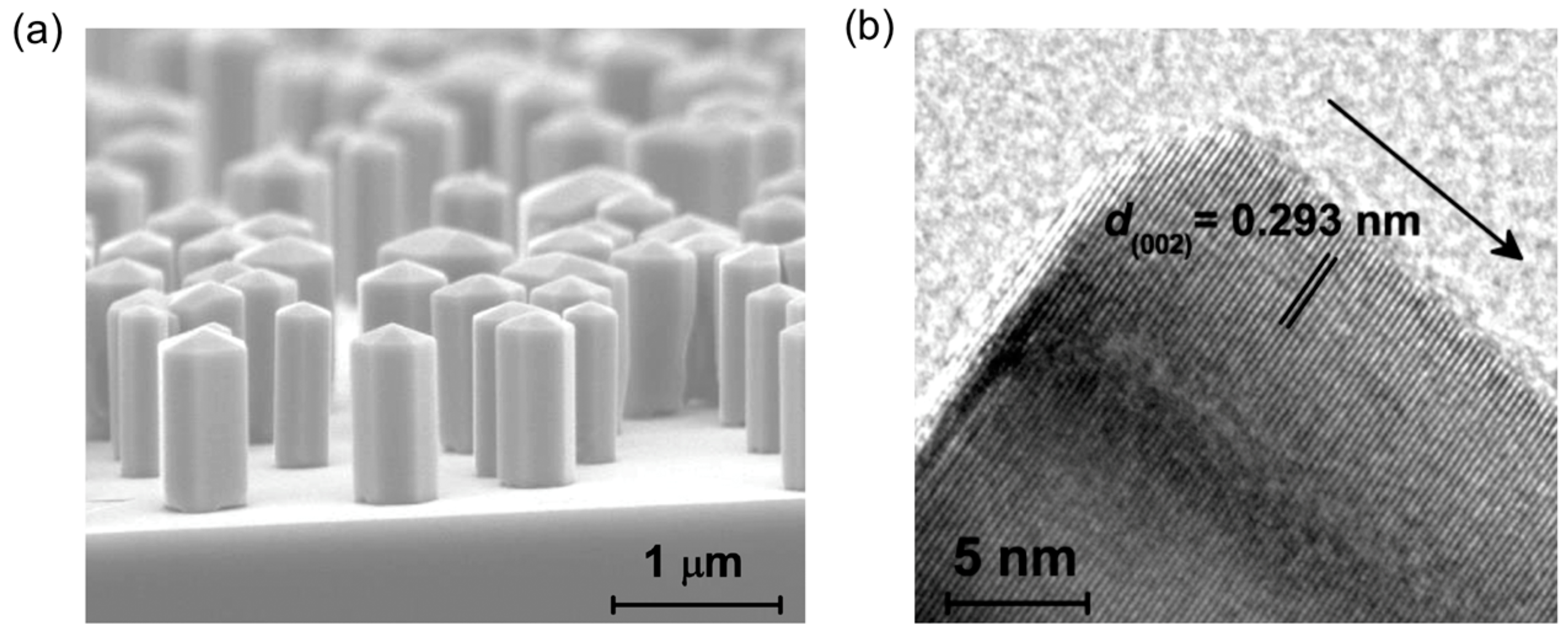
Figure 3.
(a) Power dependent photoluminescence spectra of Mg-doped InN nanowires measured at 7 K; (b,c) Extracted integrated intensity and peak energy for two peaks as shown in (a). Red triangles are for the low-energy peak, and blue circles are for the high-energy peak. Dash lines are guide-for-eye [71].

Figure 4.
(a) Near-surface Fermi-level (EF) measured by XPS for Mg-doped InN nanowire samples with different doping concentrations; (b) First principle calculation of the In-substitutional Mg formation energy. The Mg position index is defined in such a way that at surface the index is 2, and towards the bulk, the index increases. A lower Mg formation energy at surface is clearly seen compared to bulk [43].

Figure 5.
(a) Schematic of Mg-doped InN nanowire back-gate field-effect transistor; (b) The corresponding SEM image. A 3rd electrode is used to estimate the contact resistance; (c) ISD vs. VSD under different VGD; (d) Transfer characteristics measured at VSD = 0.05 V. The line is a linear fit. The arrow marks the conduction minimum [43].

Figure 6.
(a) Schematic of a single InN nanowire p-i-n LED; (b) SEM image of a fabricated device; (c) The I-V characteristics measured at 77 K; (d) Integrated light intensity vs. injection current measured at 77 K, with the inset showing a spectrum measured at an injection of 0.5 mA. The line is guide-for-eye [70].
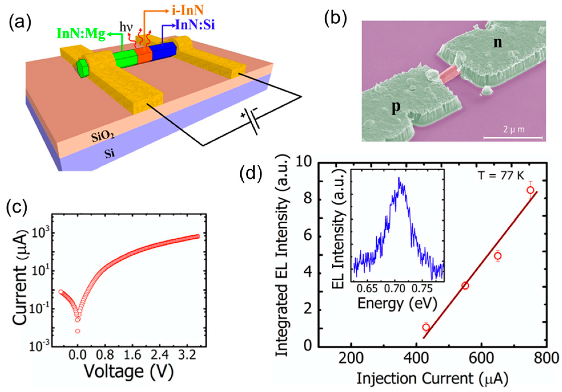
Figure 7.
(a) SEM image of Mg-doped AlN nanowires; (b) Photoluminescence spectra of Mg-doped AlN nanowire samples measured at 20 K. As the Mg-doping concentration increases, Mg-acceptor related radiative recombination becomes more pronounced (from the top spectrum to the bottom spectrum) [85].
Figure 7.
(a) SEM image of Mg-doped AlN nanowires; (b) Photoluminescence spectra of Mg-doped AlN nanowire samples measured at 20 K. As the Mg-doping concentration increases, Mg-acceptor related radiative recombination becomes more pronounced (from the top spectrum to the bottom spectrum) [85].

Figure 8.
(a) Schematic of Mg-doped AlN nanowire back-gate field-effect transistor; (b) The corresponding SEM image; (c) ISD vs. VSD under different VGD measured at 500 K; (d) The corresponding transfer characteristics with VSD = 0.2 V. The line is a linear fit [87].
Figure 8.
(a) Schematic of Mg-doped AlN nanowire back-gate field-effect transistor; (b) The corresponding SEM image; (c) ISD vs. VSD under different VGD measured at 500 K; (d) The corresponding transfer characteristics with VSD = 0.2 V. The line is a linear fit [87].
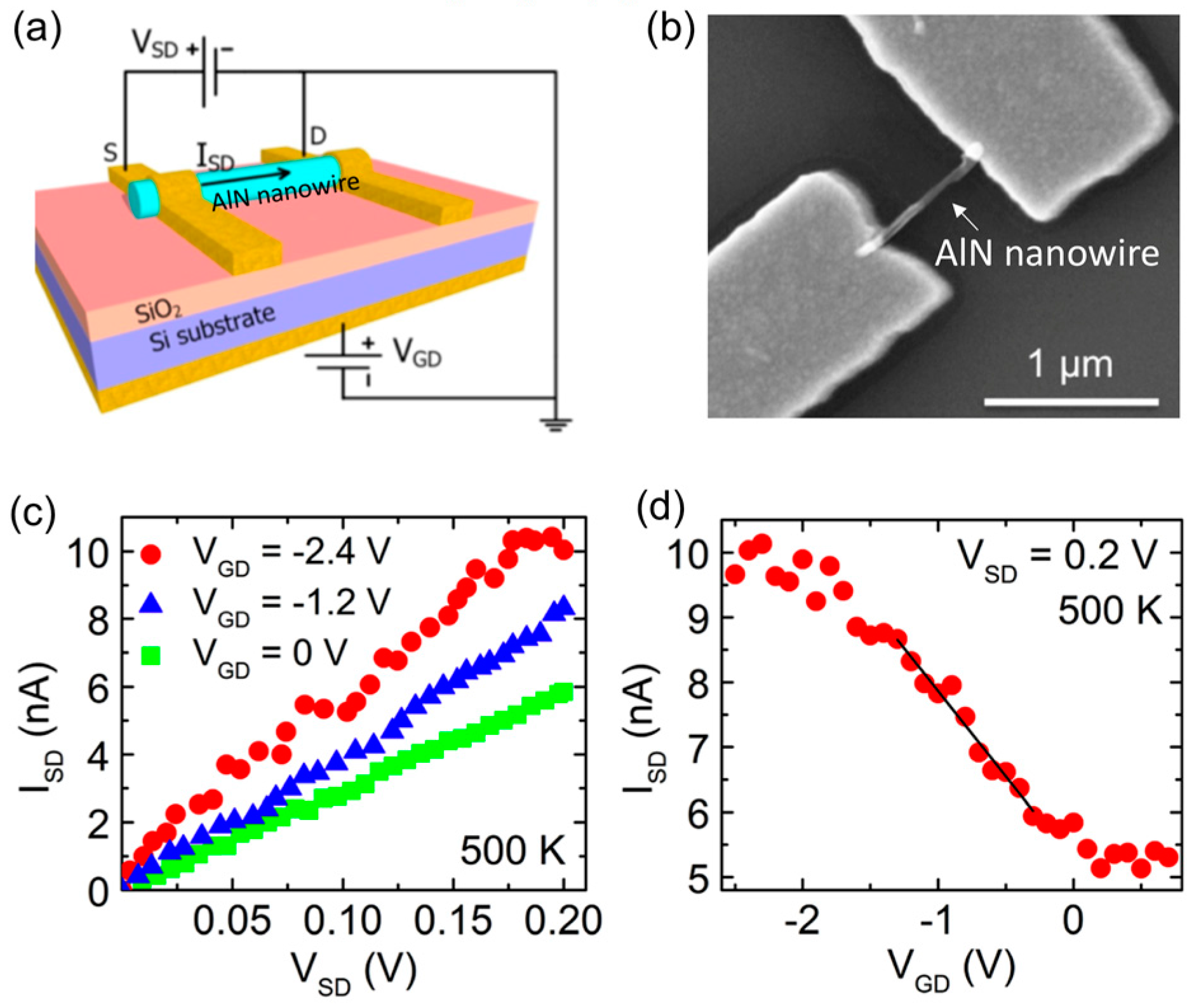
Figure 9.
(a,b) Hole mobility and concentration vs. temperature for Mg-doped AlN nanowires with different doping concentrations. The lines are linear fits [87].
Figure 9.
(a,b) Hole mobility and concentration vs. temperature for Mg-doped AlN nanowires with different doping concentrations. The lines are linear fits [87].

Figure 10.
(a) Schematic of AlN nanowire LEDs; (b) I-V characteristics measured at different temperatures, with the inset showing the room-temperature I-V characteristics in a semi-log scale; (c,d) Emission spectra measured at room temperature and 77 K, respectively [84].
Figure 10.
(a) Schematic of AlN nanowire LEDs; (b) I-V characteristics measured at different temperatures, with the inset showing the room-temperature I-V characteristics in a semi-log scale; (c,d) Emission spectra measured at room temperature and 77 K, respectively [84].

Figure 11.
(a) Schematic of light localization effect in randomly arranged AlGaN nanowire structures; (b) In-plane electrical field distribution for a TM polarized light at 240 nm; (c) Out-of-plane electrical field profile and the effective refractive index variation along the nanowire growth direction (c-axis) [94].
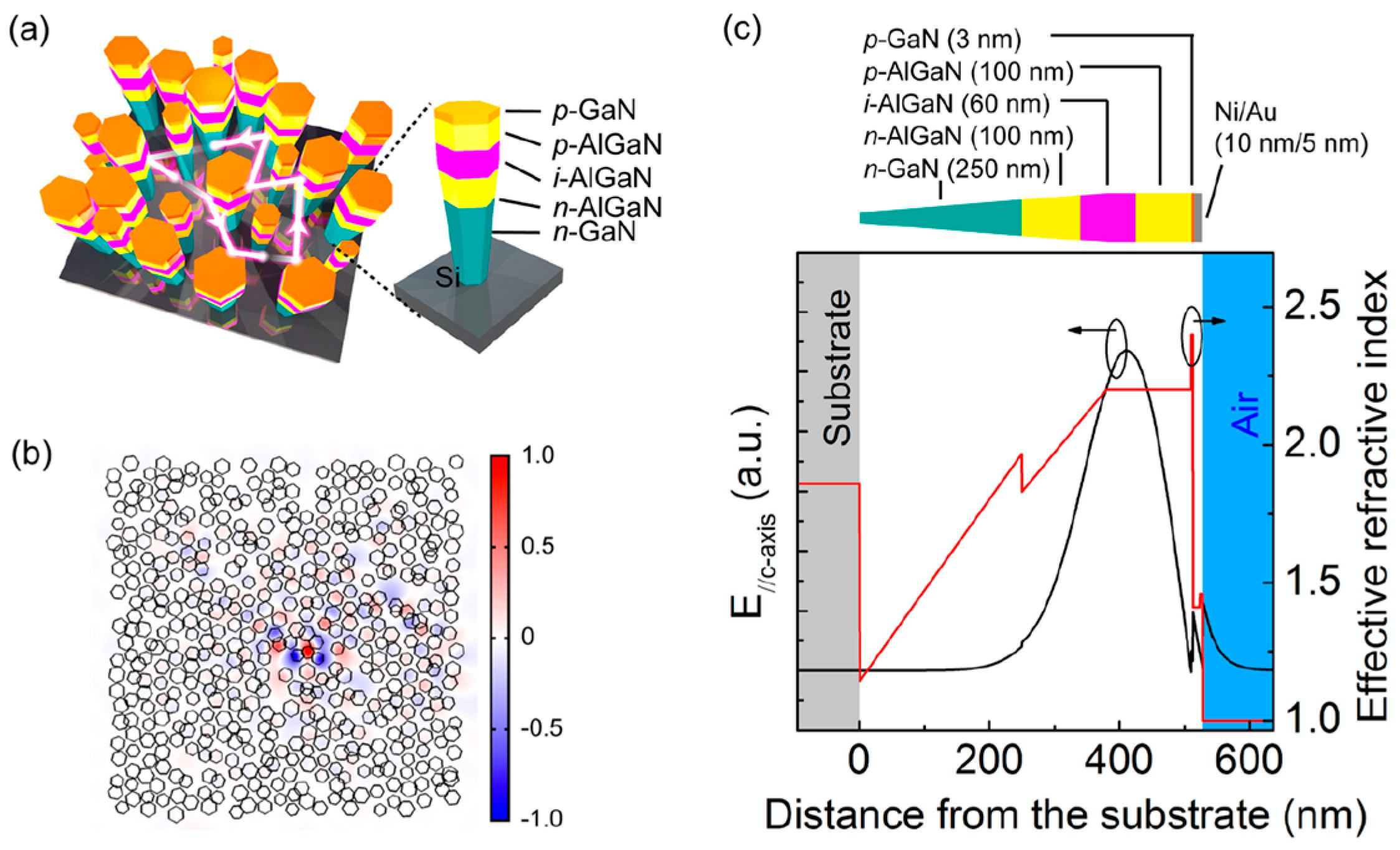
Figure 12.
(a) Lasing spectra at 239 nm measured from randomly arranged AlGaN nanowire structures; (b) Light output vs. injection current for the lasing peak and a non-lasing cavity mode from the boxed region in (a). The inset shows the light output vs. injection current for the lasing peak in the logarithmic scale; (c) Linewidth of the lasing peak vs. injection current [94].


© 2017 by the authors. Licensee MDPI, Basel, Switzerland. This article is an open access article distributed under the terms and conditions of the Creative Commons Attribution (CC BY) license (http://creativecommons.org/licenses/by/4.0/).
Share and Cite
MDPI and ACS Style
Zhao, S.; Mi, Z. Recent Advances on p-Type III-Nitride Nanowires by Molecular Beam Epitaxy. Crystals 2017, 7, 268. https://doi.org/10.3390/cryst7090268
AMA Style
Zhao S, Mi Z. Recent Advances on p-Type III-Nitride Nanowires by Molecular Beam Epitaxy. Crystals. 2017; 7(9):268. https://doi.org/10.3390/cryst7090268
Chicago/Turabian StyleZhao, Songrui, and Zetian Mi. 2017. "Recent Advances on p-Type III-Nitride Nanowires by Molecular Beam Epitaxy" Crystals 7, no. 9: 268. https://doi.org/10.3390/cryst7090268
Note that from the first issue of 2016, this journal uses article numbers instead of page numbers. See further details here.