Abstract
Below K the quasi-one-dimensional charge-transfer salt (TMTTF)SbF undergoes a pronounced phase transition to a charge-ordered ground state. We have explored the non-linear and photoconductive behavior as a function of applied voltage, laser pulse energy and temperature. Besides a decay of the photoconductive signal in a double exponential fashion in the millisecond range, we discover current oscillations in the kHz range induced by the application of short laser pulses. While the resonance frequencies do not depend on voltage or laser intensity and vary only slightly with temperature, the amplitude changes linearly with the laser intensity and voltage. We suggest that photo-induced fluctuations of the charge-ordered state alter the current flow of the single particles and hence, the photocurrent. The findings are discussed and compared to comparable phenomena in other low-dimensional electron systems.
Keywords:
charge-transfer salts; TMTTF; charge-order phase transition; non-linear transport; photoconductivity; current oscillations; calculations of band structure and optical conductivity PACS:
77.84.Jd; 77.80.Fm
1. Introduction
The charge-transfer salts (TMTTF), where TMTTF stands for tetramethyltetrathiafulvalene and X for a monovalent anion, have been under scrutiny due to their quasi-one-dimensional electronic character and ordering phenomena in the spin and charge sectors [1,2,3,4]. In recent years, several comprehensive investigations have been conducted on the optical [5,6,7,8,9] and transport properties [10], the lattice [11,12] and electronic structure [13,14,15] as well as on the magnetic properties [16,17,18,19,20,21]. However, not much is known about the non-linear properties at the charge-order transition taking place at K and transient conduction phenomena. This is surprising, since nonlinear behavior was observed in various inorganic as well as organic compounds in the vicinity of a metal-insulator transition, such as the charge-density wave transition in NbSe, the metal insulator transition in VO, or the charge-order transition in the two-dimensional -(BEDT-TTF)I salt [22,23,24,25,26,27,28,29].
Several classes of electrically induced nonlinear phenomena in solid-state materials can be distinguished:
- Non-equilibrium charge carriers: modification of the charge carrier number or the mobility.
- Space-charge distribution: for instance impurity bands.
- Electrically induced phase transitions: modification of the electronic system or the crystalline structure.
- Ionic motion in the host material: forming of conductive filaments.
- Sliding charge density waves or charge order.
- Domain wall motions or excitations of solitons.
Although exotic electrically induced effects emerge in most classes of materials, it is basically impossible to draw a conclusive picture since the diversity of the involved ground states is enormous. Nevertheless, in regard to future electronic devices and applications, more effort has to be devoted to the experimental studies on electrically induced phenomena as well as the development of accurate models explaining a wide range of these effects occurring in various material classes. For a broader discussion we refer to the review articles [30,31] and textbooks [32,33] and further literature listed therein.
The first studies on electrically induced phenomena in organic conductors were performed in the 1970s and 1980s on Cu(TCNQ) [34] and TTF-CA [35]. Later, this was extended to other organic systems, such as K(TCNQ) [36], where the switching was also recorded optically, expressing a stripe structure of alternating insulating and metallic domains between the two contacts. In the two-dimensional organic salt -(BEDT-TTF)CsZn(SCN) [37] and its sister compounds [38] the charge order was melted by applying a current to the crystal [31]. To date, no concept or model could be established that can explain all these observations in organic salts.
Since nonlinear behavior was observed in several different inorganic as well as organic compounds at the vicinity of a metal-insulator transition, we expect similar phenomena in the quasi one-dimensional salts (TMTTF), with the centrosymmetric anion PF, AsF, and SbF. In Figure 1 we collect the important experimental findings characterizing these three materials. Upon cooling the resistivity goes through a shallow minimum due to electronic localization and later exhibits a kink at the charge-order transition , as displayed in panel (a). No significant change is observed in the magnetic susceptibility at [17] plotted in Figure 1b; while the magnetic order and spin-Peierls transitions occur at low temperatures. Due to charge order, the dielectric constant exhibits a maximum at this temperature (see panel (c)), more or less following Curie’s law [40]. As presented in Figure 2, the charge-sensitive vibrational modes split due to charge disproportionation [7]; similar conclusions are drawn from the NMR spectra [41] plotted in Figure 1d.
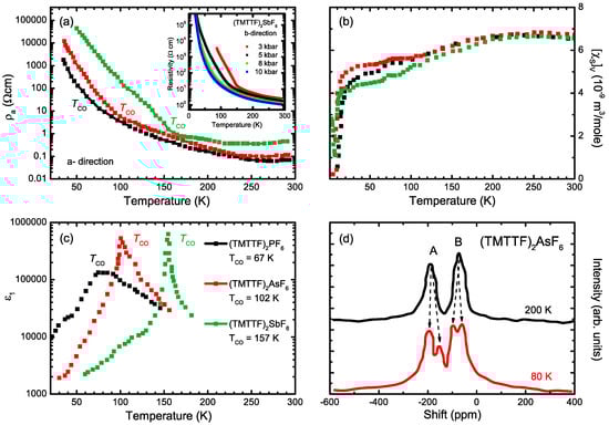
Figure 1.
Experimental characterization of (TMTTF), PF (black), AsF (red), and SbF (green) single crystals. (a) Temperature-dependence of the resistivity along the a-direction [10]. The labels mark the charge-order transition temperature , 102, and 157 K, respectively. The inset demonstrates the effect of hydrostatic pressure on the transition by displaying the temperature-dependent dc resistivity of (TMTTF)SbF measured along the b-direction. is seen as a kink in that shifts to low temperatures as pressure increases; (b) Temperature-dependence of the spin susceptibility at constant volume . (TMTTF)PF and (TMTTF)AsF undergo a spin-Peierls transition at K and 13 K, respectively. (TMTTF)SbF exhibits an antiferromagnetic state below 8 K causing an increase of . Above the transition can be described by a model of a 1/2 antiferromagnetic Heisenberg chain [16,39]; (c) The real part of the dielectric constant maesured at kHz as a function of temperature T reveals a Curie-law behavior [40]; (d) C-NMR spectra of (TMTTF)AsF at 200 K and 80 K. Above K two distinct features A and B can be identified due to the two molecules per unit cell. They split into a total of four peaks, as depicted by the arrows [41], giving evidence for charge order.
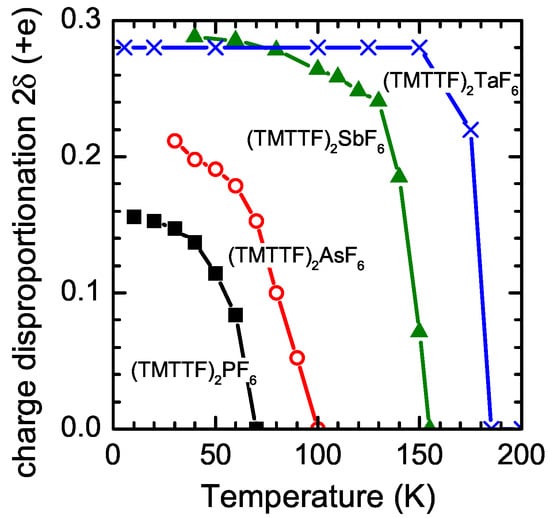
Figure 2.
Temperature dependence of the charge dispropotionation probed by the splitting of the infrared-active molecular vibrational mode in (TMTTF) with PF, AsF, SbF and TaF as a function of temperature T recorded along the c axis. The charge imbalance 2 is estimated from the difference of the two resonance frequencies by [7,42].
In Figure 3a the optical reflectivity of (TMTTF)SbF is plotted as measured for ambient conditions with the electric field polarized parallel to the chain direction. Using the Kramers-Kronig relation the frequency dependent conductivity can be calculated as illustrated in the lower panel (b). The spectra are dominated by a strong band around 2000 cm due to excitations between the Hubbard bands, which occur due to electronic correlations. In addition emv-coupled vibrational features strongly affect the optical properties in this range of frequency [43,44].
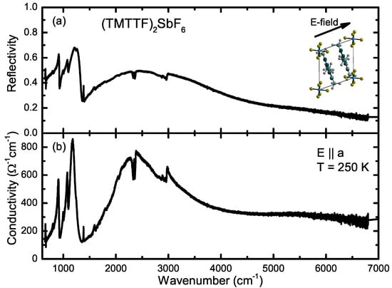
Figure 3.
Frequency-dependent optical reflectivity (a) and conductivity (b) of (TMTTF)SbF along the crystallographic a direction measured at K.
For (TMTTF)SbF a surprising behavior of the material was observed in response to electrical and optical pulses, which is presented and discussed below in detail. We could not detect similar phenomena in (TMTTF)PF and (TMTTF)AsF. As depicted in Figure 1a (TMTTF)SbF reveals the steepest slope at the phase transition, while (TMTTF)PF and (TMTTF)AsF exhibit a smooth transition. Therefore, we conclude that for the one-dimensional salts strong resistivity changes [10] at the transition temperature are a good indication that nonlinear behavior can be observed. Otherwise, the difference is too small and the photo-induced effect is absent.
2. Experimental Details
Single crystals of the charge-transfer salts (TMTTF)SbF were grown by electrochemical methods as described previously [10,39]. The needle-shaped single crystals are several millimeters long in the a-direction and less than a millimeter wide in the other crystal directions. Figure 4 shows the crystal structure of (TMTTF)SbF in different orientations.
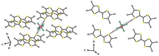
Figure 4.
Two views on the crystal structure of (TMTTF)SbF illustrate the confinement of the octahedral anions in a cavity formed by methyl groups (gray) of the surrounding TMTTF molecules. Also shown by dashed lines are the closest connections between the fluorine (green) and sulphur atoms (yellow); the antimony ion (red) is located in the center octahedron.
For transport experiments along the chain direction a four fine gold wires were attached to the crystal by carbon paste as contacts. The Ohmic nature of these contacts on the organic crystals has been verified in detail previously [10,25,45]. The samples were cooled in a helium cryostat. Besides simple characterization (cf. Figure 6), we measured the transport response of the crystals along a, when a strong electric pulse is applied.
In a second step, photoconductivity was studied, i.e., we probed the time response of the electric transport after exposing the crystal to a laser pulse (8 ns) with a wavelength of nm (corresponding to a photon energy of 2.33 eV). The setup for the photocurrent measurements sketched in Figure 5b consists of two contacts on the specimen separated by 1.1 mm. A voltage pulse with variable width is created on the contacts by a pulse generator. The applied voltage U and current are measured by an oscilloscope. Since the laser has a low repetition rate between 1 Hz and 20 Hz heat accumulation is avoided; it is also ensured that long living states decay before the next pulse arrives and hence, accumulation effects can be excluded.
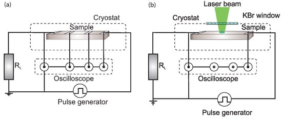
Figure 5.
(a) For the time-resolved transport measurement either the four-point or two-point configuration was employed. It can be switched between the steady-state and the time-resolved transport measurement. The voltage pulses are created by an Avtech AV-1010 B of Hewlett-Packard HP 214B pulse generator. A Tektronix TDS 744A oscilloscope (input impedance 1 M) records the applied voltage U, the voltage drop across the inner contacts as well as the total current of the circuit by the voltage drop across the load resistor in series; (b) Schematic drawing of the photoconductivity setup. It consists of a pulse generator creating the voltage U at the sample, an oscilloscope, and a load resistor. is used to determine the current in the circuit. The frequency doubled Nd:YAG laser beam is focussed through the cryostat window. The beam diameter is approximately 0.6 mm, the laser intensity ranged up to 5 mJ/cm.
The generated photocurrent can be derived from the following physical relation. The electronic circuit consists of a voltage source, the sample and the load resistance . The dark current is defined as
the dark resistance of the sample and the corresponding resistance when illuminated. The total current under illumination is respectively
with Thus, the measured photocurrent is
In a photocurrent measurement the contact resistance plays a crucial role since it influences the transport of the charge carriers to the contact. The materials, i.e., metal, semiconductor or insulator, touching at the interface form different types of contacts. At the boundary the band structure is deformed due to the difference in work function and electron affinity of the materials. Therefore, a barrier is created at the boundary surface leading to a depletion area [32,46]. By that, additional carriers can be transferred or the charge carriers can be blocked at the contacts. There are typically two kinds of contacts: the Schottky-contact and the Ohmic contact. Generally, several processes contribute to the charge transport across the barriers. The dominating processes are the thermal emission of charge carriers across the energy barrier and tunneling of the carriers, being temperature-independent. However, it is assumed that Ohmic contacts are formed in the organic crystals, based on previous studies [10,25,45]. During the transport measurements the temperature-dependence of the contacts was checked by measuring the contact resistance at specific intervals; to that end, we switched between four-point and two-point resistance measurements, as depicted in Figure 5a. Their resistance value normally changes at a phase transition when a gap opens in the electronic system. For details on the time and field-dependent experiments we refer to Refs. [47,48].
3. Response to Electric Fields
Before discussing the response of (TMTTF)SbF to electric pulses, let us consider the temperature-dependent resistance from room temperature down to 125 K, in order to determinate the phase transition temperature. This allows us to assign more precisely compared to optical methods [7,8] and to deduce the contact resistances in this particular case. In Figure 6 the logarithm of the resistance of (TMTTF)SbF is illustrated for the a-direction in a temperature range from room temperature down to 125 K. When lowering the temperature, the resistance decreases down to a minimum at K, which corresponds to the sign change of its slope (see inset). This is caused by electron-electron interactions opening up a Mott gap at the middle of the upper half-filled band and Umklapp scattering. Thus, the resistance further increases with decreasing the temperature down to the charge-order transition, corresponding to a linear slope of the derivative. At a kink arises and below this temperature increases nonlinearly; hence transport is not just thermally activated. It is worth mentioning that for (TMTTF)SbF the resistivity increases more abruptly and steeper at the charge-ordered phase transition than observed in the (TMTTF)PF and (TMTTF)AsF analogues. Furthermore, (TMTTF)SbF reveals an anomaly in the thermal expansion coefficient at the charge-order transition [49]. In contrast, in its sister compounds no feature appears at the corresponding transition temperature.
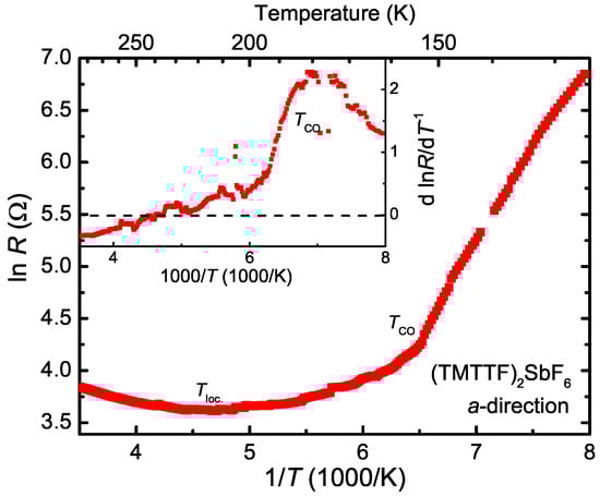
Figure 6.
Logarithm of the resistance of (TMTTF)SbF as a function of the inverse temperature . At about K a minimum appears, marking the transition to the localized state related to the opening of a Mott gap. The resistance increased slightly and at K a kink is observed in the curve due to the charge order transition. Inset: derivative of the logarithm of the resistance vs. . The charge localization leads to a change of the sign from negative (metallic) to positive (insulating). Also the slope changes at leading to a rather flat curve at low temperatures.
A similar behavior appears in the temperature-dependent evolution of the charge disproportion [7], as depicted in Figure 2. While in (TMTTF)PF and (TMTTF)AsF a mean-field behavior appears, a first-order-like transition takes place in (TMTTF)SbF. The latter is probably related to the enhanced dimerization (see [10,12]) and the charge localization state at elevated temperatures. This behavior is even more pronounced in (TMTTF)TaF, where the phase transition takes place at K and is of comparable size [42].
It is interesting to recall early studies on the electronic transport in quasi-one-dimensional organic conductors, such as TTF-TCNQ, TMTSF salts and TMTTF salts in the metallic and insulating states that occur below charge- and spin-density-wave or charge-order transitions [1,2,50,51,52,53,54,55,56,57,58,59]. There the current flow in strongly anisotropic metals, fluctuations, non-linearity, contact issues, etc. are discussed in depth.
We now apply voltage pulses of 1 ms duration to the sample and measure the total current and the voltage drop across a load resistor of k connected in series to the sample. In Figure 7 the time-dependent current response of (TMTTF)SbF at K is plotted for two different voltages. At the beginning of the pulse, an overshoot of the measured current occurs due to the parasitic capacity and resistance in the circuit (panel a). The short oscillating signal located at s is caused by a parasitic current induced by the switching of the Pockels cell of the laser system, later used to create the photocurrent. For low voltages ( V) the current signal stays constant during the whole pulse. When increasing the amplitude of the pulse, the current increases approximately in a linear way obeying Ohm’s law. Nevertheless, following the temporal evolution further reveals a nonlinear increase of the current, which can be attributed to a thermal modification of the contact resistance.
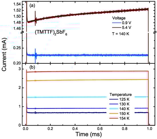
Figure 7.
(a) Response of the current in (TMTTF)SbF, when 1 ms pulses of two different voltages are applied at K; (b) Current response plotted for various temperatures below .
Figure 7b displays current pulses for different temperatures below . The current signal is reduced for the same applied voltage in the same way as the total resistance increases with temperature. Independent on the applied voltage or examined temperature no switching behavior or current oscillation can be detected that would indicate a sliding of the charge-density wave (CDW) or a collective response of the charge-ordered state [60,61].
4. Response to Laser Pulses
Next the photo-response of (TMTTF)SbF was studied by illuminating a fraction of the space between the two contacts by a laser pulse. In Figure 8 the recorded current pulse is illustrated exemplarily at K for a 5 V voltage pulse and a laser pulse with the energy of 40 J. Similar to Figure 7, an overshoot is present at the beginning. Additionally, 750 s after the onset of the voltage pulse, the current suddenly shoots up with a rise time a few nanoseconds. Strikingly, this onset is correlated with the incident laser pulse, giving clear evidence for photoconductivity. The signal barely decays and stays almost constant over the entire voltage pulse length. In the inset of Figure 8 an enlarged detail of the first 400 s of the photocurrent is visualized. Surprisingly, current oscillations are superimposed on top of the signal, whose amplitude decays with time. The inset further reveals a slight signal decay within the first 59 s.
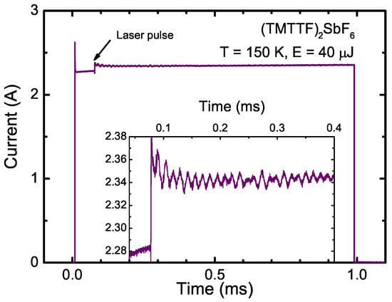
Figure 8.
Current response to a 1 ms long 5 V voltage pulse applied on a (TMTTF)SbF crystal at a temperature of 150 K. At about ms, an additional laser pulse of s (black arrow) illuminates the sample. This induces a photocurrent, visible in the steep, weak jump of the current signal. In the inset the first 400 s of the photocurrent response are magnified. Interestingly, overall signal is are superimposed with pronounced oscillations.
We examined the photocurrent signal for various voltages below the phase transition K, as presented in Figure 9a for the temperature K and laser pulse energy J. Above , no change was observed. There, the photocurrent was extracted by subtracting the current without any light (see for example Figure 7) from the total current signal. Thereby we can also eliminate the nonlinear transport behavior of the device, consisting of the contact resistance and the sample. By enlarging the applied voltage the signal increases linearly. Similarly, the photocurrent becomes larger with rising laser pulse energy and the temporal behavior is the same as for the voltage-dependent current curves, as depicted in Figure 9b. Finally, also the temperature dependence of the transient photocurrent is plotted for a fixed pulse energy 32 J and voltage amplitude V in Figure 9c. The photocurrent is the smallest in the vicinity of the phase transition ( K) and then stays almost constant below K. One should note that all curves in the latter three graphs exhibit the same temporal dynamics, which can be fitted by a double-exponential decay function . Between K and 125 K, the first time constant decreases from 30 s to 16 s and diminishes by a factor of 2 from 300 s to 170 s. Here is the background which can be considered as a third extended living state, decaying at least on a millisecond time range. Such relaxation dynamics have also been observed in other photo-response experiments on organic conductors [62,63,64,65] taking place between the microsecond regime and far above the millisecond time scale.
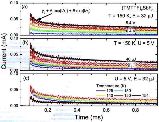
Figure 9.
Time-dependent photocurrent of (TMTTF)SbF for (a) various voltages; (b) laser pulse intensities and (c) temperatures as indicated. In all three panels the temporal dynamic is fitted by a double exponential function (black lines).
However, the most important phenomena are the interference patterns which are superimposed on top of the exponentially decaying current signal. To the best of our knowledge, this has never been detected before in a photoconductivity experiment on organic conductors. In order to analyze the oscillations in detail, the frequency components were extracted from the decaying current by fast Fourier transformation (FFT). The amplitudes of the frequency components from the curves, depicted in Figure 9, are visualized in Figure 10 for various parameters. Five resonance frequencies can be identified: 49 kHz (labeled A), 54 kHz (B), 58.5 kHz (C), 77.5 kHz (D), and 82 kHz (E). Varying the voltage does not influence the resonance frequency (panel a), although the amplitude increases linearly. The same is true for the laser intensity dependence of the oscillation amplitude; it increases linearly without any modification of the peak positions, as shown in Figure 10b for K and V. It is important to note that the dark current (J laser power) is independent of the applied voltage, as it is exemplarily displayed in Figure 7; no oscillations occur, resulting in a flat amplitude spectrum. While the resonances display only an amplitude-dependence on the voltage and pulse intensity, both the amplitude as well as the resonance frequency change with temperature.
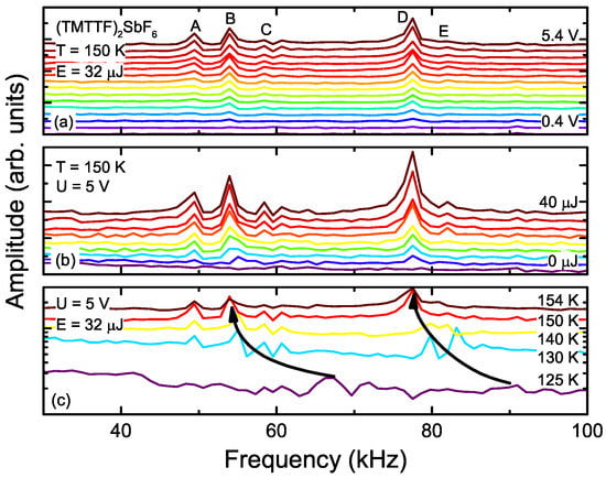
Figure 10.
Amplitude spectra of the current oscillations in (TMTTF)SbF obtained by fast Fourier transformation. The curves are shifted by a constant value for better visualization. Amplitude spectrum in a frequency range from 30 kHz to 100 kHz plotted (a) for various voltages from V to 5.4 V and for a laser pulse energy of 32 J at 150 K; (b) Same temperature and frequency range as in (a), however, the amplitude spectra are shown for different laser pulse energies at a fixed voltage of 5 V. (c) Temperature-dependent amplitude spectra from K to 125 K for 32 J and 5 V. The black arrows indicate how the current oscillations shift in frequency as the temperature is raised.
5. Discussion
We now turn to the question of the origin of the photocurrent and its dynamic: Why does the current oscillate after illumination?
Iwase et al. proposed a phenomenological description [66,67] relating to the temperature and electric current, , where the first term on the right side describes the thermal activated linear Ohmic behavior and the second term accounts for the nonlinear conductivity. A two-state model assumes that “hot electrons” are generated in the conduction band similar as in inorganic semiconductors. Mori and collaborators [68,69] successfully applied this approach to -(BEDT-TTF)(HSO) and (TMET-TTP)PF. The electron system is assumed to be decoupled from the lattice; hence an effective electron temperature can be defined. Note, this is just the temperature of the hot electrons and does not mean that the sample is heated up. The electron-electron interaction is much faster than the electron-phonon interaction [28]. These excited electrons or quasi-particles follow the heat balance equation:
which can be simplified by assuming a linear spatial heat transfer, expressed by the last term, leading to:
The left side of the equation is the energy stored in the excited electronic system. The first term on the right hand side is the electric input power P in Wcm created by the externally applied electric field or current, which can be expressed as follows:
and the second term of Equation (5) describes the linear heat transfer from the electronic system to the lattice, which is kept at the initial temperature . Here is the thermal conductivity of the electron system and the electron heat capacity per volume. Equation (5) is solved numerically for a certain starting electric field or current pulse. In general is determined from the conductivity curve of the corresponding material because the excited carriers are responsible for the dc conductivity. From this model, a delay time can be estimated which also accounts for current oscillations. A more detailed discussion of the two-state model can be found in Ref. [28,68,69].
The possible influence of thermal effects on the induced current has to be discussed. Following the approach presented in Ref. [28,70], we calculated the temporal behavior of the sample temperature and correlate it with the temperature-dependent sample resistance depicted in Figure 6. The result of the simulation is visualized in Figure 11 for various temperatures T between 125 K and 154 K. We assume that the complete pulse energy is absorbed and transferred into Joule heat at the surface of the specimen as the penetration depth is only a few hundred nanometers. Besides that, the lateral electric field is strongest between the contacts. Thus, we are most likely probing a thin layer at the surface. From this simulation, a very sharp increase of the current would result; which actually is not the case in the presented experimental curves. The relaxation dynamics or cooling process is very fast and related to an extreme drop of the photocurrent within 1 s. Afterwards, it asymptotically approaches zero. Comparing the experimental results with the theoretical findings, it is clear that the amplitudes and time constants of the signals are different. Only in the case of the long relaxation process a thermal effect may contribute to the photocurrent signal. Furthermore, the simulation does not reveal any current oscillations, which supports the view that instead the system is driven into a metastable condition different from a simple heating scenario.
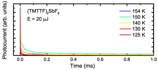
Figure 11.
Simulation of a thermally induced photocurrent by a short laser pulse for five different temperatures as indicated. A steep current peak slowly relaxing to zero.
For our case of (TMTTF)SbF, the laser photons with eV excite either the transition from the quarter-filled HOMO band to the LUMO+1 band of the TMTTF molecules or the transition from a fully occupied band far below the Fermi energy to the quarter-filled unoccupied mid- infrared band, as depicted for the transitions labeled by I in Figure A3 of the Appendix A.2. After the vertical electronic excitation into the unoccupied bands, several decay channels are open:
- A free electron and hole can be created, which get separated from each other by the electric field, leading to the photocurrent signal. However, they can recombine before they reach the electrodes or become trapped. In general, the lifetime of free carries is between nanoseconds and microseconds.
- After a few picoseconds the excited electronic states couple to the lattice phonons and intramolecular vibrations. By this, energy is transferred to the lattice subsystem and the sample is warmed up.
- Afterwards, the excited electrons decay back into their initial state by emitting a red-shifted photon. The latter can be reabsorbed or detected as a photo-luminescence signal. Also, a radiation-free decay is possible into the lowest excited (mid-infrared) band.
- Otherwise, the excited charge can relax into a low-lying unoccupied band, triggering a charge transfer from one cation to its neighboring molecule in the picture of a molecular chain. This can induce a phase transition from the charge-ordered to the metallic state.
- Recently, in photo-luminescence spectra of a two-dimensional organic Mott insulator the creation of an exciton was suggested [71]. The theory of photo-induced transitions [72] proposes that higher excited states can be populated and excitons brake up; Frenkel excitons becomes charge-transfer excitons and propagate. The separation of excitons may also stimulate a light-induced transition. Especially in low-dimensional system fluctuations as well as electron-electron and electron-phonon interactions play a crucial role, eventually destabilizing the equilibrium state. This picture is similar to the model suggested for the photo-induced phase transition in TTF-CA [70,73].
While in Figure 8 and Figure 9 the laser pulse hits the sample after the voltage is applied, we now delay the voltage pulse with respect to the laser pulse; in Figure 12 the photocurrent signal is displayed for different delay times of the voltage pulse. For more than 0.8 ms delay time the signals overlap with each other. Interestingly, the oscillations persist even when the voltage pulse is applied long after the light irradiation; but with a smaller amplitude. Moreover, the oscillations appear still at the same position, which proves that they are rigidly linked to the light pulse. It is surprising that the current curves are strongly displaced with respect to each other, indicating that without an external electric field, the excited free electrons and holes (or excitons) are not separated from each other and hence, recombine rapidly. In the case of a pure thermally induced effect, the current dynamics or the resistance, respectively, is expected to be independent of the applied voltage and to exhibit the same temporal behavior, regardless of the delay time between laser pulse and voltage pulse.
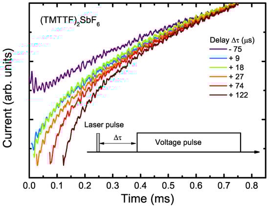
Figure 12.
Raw data of the photocurrent signal measured for (TMTTF)SbF for various delay times between the voltage and 8 ns laser pulse for a laser energy of J and V at K.
At this point, we should recall similar effects detected over the last fifty years in other compounds with and without illumination.
- In the 1960s and 1970s transport measurements on silicon with two Schottky contacts revealed current oscillations in the kHz regime, which were ascribed to double current injection at the contacts [74]. However, the frequency could be varied by changing the voltage bias or temperature and the oscillations occur only above a critical threshold field [75].
- The well-known creation of hot or non-equilibrium electrons in semiconductors such as GaAs [33] leads to electric field-dependent charge carrier velocities, causing a negative-differential resistance. One of the related phenomena is the famous Gunn effect, yielding current oscillations in the microwave regime. In this case, the frequency can be tuned by the sample length or by the applied voltage.
- Similar to the negative-differential resistance current oscillations in pure semiconductors, self-oscillating (photo-)currents were observed in superlattice structures, consisting of two different direct semiconductors such as GaAs-AlAs [76]. Due to the different energy levels in the quantum wells and the tunneling effect between the layers, a negative differential velocity regime is created as a function of the external electric field. The electric field reveals a spatial variation within the superlattice structure. Thereby, the different regions separated by domain walls get unstable and hence cause the oscillations. The resonance frequency can be tuned by the bias voltage or laser power [77,78].
- Current oscillations occur frequently in nonlinear transport studies in various organic conductors [38,45,79,80,81,82,83]. There, they are often related to sliding charge-density waves (CDW) or electrically induced insulator-metal transitions accompanied by a bistability [60,79].
- It is known that ferroelectric materials render a modification of the polarization by light stimulation, which can be detected by photoconductivity measurements [84]. Here, the detected signal is generally composed in of three different terms [85,86,87]: first, a fast decay of the excited states within a few microseconds, in addition a pyroelectric signal that can last several milliseconds, and finally piezoelectric oscillations superimposed on the decaying current due to the thickness variation of the sample by sound waves. Since the Fabre salts are charge-ordered ferroelectric crystals [50,88], they resemble the behavior of well-known inorganic ferroelectric, such as LiNbO.
- Above a certain threshold field, voltage oscillations (in the range of a few 100 mV/cm) occur in CDW systems [50,60], such as NbSe, TaS or KMoO, which are attributed to the collective sliding of the charge density wave. There, the resonance frequency depends on the applied voltage and temperature. However, only very few photoconductivity studies were conducted on CDW materials [89,90]. Experiments utilizing a lock-in technique do not directly provide the time-dependent behavior of the photocurrent. It was reported that the threshold voltage between the creeping and sliding state of the CDW can be raised by increasing the light intensity.
While the first four possibilities have already been disregarded as a possible origin of the current oscillations in our study, let us discuss the remaining suggestions. (TMTTF)SbF can be considered as a one-dimensional charge-ordered ferroelectric, and the temporal dynamics of its photocurrent resembles that of illuminated inorganic ferroelectric crystals. For these, the current oscillations are related to the speed of sound in the bulk material. In our case a sample length of 2 mm and a resonance frequency of 77.5 kHz would lead a sound velocity of 155 m/s. This is one order of magnitude below the speed of sound (2500 ms) previously reported [91,92,93]. Hence light-induced sound waves can be ruled out as origin of the observed oscillations.
The most appealing explanation of current oscillations in the charge-ordered state of (TMTTF)SbF starts with a 4k-CDW. In general a coherent sliding of the density wave is observed above a more or less well defined electric threshold field of a few mV/cm [50,60]; this is not the case for (TMTTF)SbF. Here we have to apply an electric field of several V/cm, much more than typically needed for classical CDW systems; but two orders of magnitude smaller than the threshold fields in the charge-ordered salt -(BEDT-TTF)I [22,28,29]. The large difference can be explained by the fact that most of the typical CDW compounds develop an incommensurate charge modulation that is pinned to impurities. Charge-ordered systems are inherently commensurate and much more rigid as far as the coupling to the underlying lattice is concerned. Furthermore, single-particle excitations should not weaken the pinning of the CDW, it may even increase the threshold field. In conventional CDW systems, photo-excitation does not facilitate sliding of the condensate. In addition, it was observed in NbSe and comparable CDW systems that the resonance frequency of the depinned 4k-CDW depends on the external voltage; in the present case of (TMTTF)SbF, however, no such effect could be identified. Further photoconductivity studies have to be performed on charge-ordered one-dimensional materials to clarify this point. Nevertheless, we suggest that our observations are caused by photo-induced fluctuations of the charge-ordered state, which alter the current flow of the single particles and hence, the photocurrent.
6. Summary and Conclusions
We report on the first study of photoconductivity and non-linear transport in quasi-one-dimensional charge-ordered compounds. The Fabre salt (TMTTF)SbF exhibits unusual conduction behavior when electric fields and light pulses are applied; we could not detect similar phenomena in (TMTTF)PF and (TMTTF)AsF. Most interesting is the time-dependence of the photoconductivity signal which reveals current oscillations in the kHz range below the charge-order transition at K. Within milliseconds after photo-excitation the signal exhibits an overall decay, in addition a faster decay process can be identified in the microsecond range. The most surprising observation, however, are oscillations superimposed on top of the photocurrent that contains several frequencies in the kHz regime. We investigate the field, laser power and temperature dependence. We discuss possible explanations of the observed photoconductivity and current oscillations; suggesting an interaction of the excited single particles and the charge-ordered state.
Acknowledgments
We acknowledge valuable discussions with Tomislav Ivek, Andrea Rohwer and Eva Rose. We thank Gabriele Untereiner. for the crystal growth and sample preparation. The project was supported by the Deutsche Forschungsgemeinschaft (DFG) and by the Carl-Zeiss-Stiftung.
Author Contributions
T.P. designed and performed the experiments and analyzed the data; M.D. and T.P wrote the paper.
Conflicts of Interest
The authors declare no conflict of interest.
Appendix A. Ab Initio Calculations
For a better understanding of the photo-induced processes in the Fabre salts, we have performed calculations of the electronic band structure and optical conductivity.
Appendix A.1. Band Structure
The band structure of (TMTTF) (with X = PF, AsF, and SbF) were determined by ab initio Density Functional Theory (DFT) calculations which is implemented in the software package Quantum Espresso [94]. In contrast to the well-established Hückel theory with its molecular orbitals, it is based upon plane-waves and it is not semi-empirical; instead, it uses the advantage of the crystal periodicity and can be applied to almost every material. Moreover, it is fast, reliable and robust. Furthermore, we used a norm-conserving PBE GGA functional for all atom types, up to a certain level taking into account the exchange correlation as well as the spatial variation of the charge density. The room-temperature crystal structure for the calculations were taken for (TMTTF)PF and (TMTTF)AsF, while for (TMTTF)SbF we performed X-ray scattering from K down to 100 K [13,14,95]; the structures were not relaxed within the calculations. Due to the stoichiometry of the organic salts, they are treated as metals. Thus, a smearing factor of 0.005 Ry was applied. Furthermore, the cutoff energy of the plane waves and the electron density were set to 30 Ry and 120 Ry, respectively. The wave functions were determined in a self-consistent way on a Monkhorst grid. The band structure was calculated on the k-path: .
The resulting band structure close to the Fermi energy is depicted in Figure A1 for K. The HOMO of the Fabre-salts is three quarter-filled. Due to the dimerization between the TMTTF molecules, the HOMO is split into a lower completely filled band and a half filled upper band. These bands are well separated from the other bands which are located at −2 eV below and about 1.5 eV above the HOMO band (not shown here). The anion layer does not contribute to the bands near the Fermi energy due to the closed shell of the anions. The occupied and unoccupied bands of the anions reside far below and above the HOMO band.
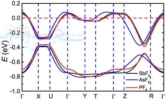
Figure A1.
Comparison of the band structure of (TMTTF), X= PF (red), AsF (blue), and SbF (black) at room temperature along the k-path: .
The dimensionality of the compounds is reflected by the band dispersion. The band shape is similar for all compounds; the main deviations occur for the paths corresponding to the b-direction ( or ). They reveal an enhanced dispersion going from the large SbF to the smaller PF anions. This is consistent with the increase of the overlap between neighboring TMTTF molecules along the b-direction, being caused by the reduced spacing between the adjacent stacks due to the smaller anion size when going from (TMTTF)SbF to the smaller (TMTTF)PF. Therefore, the compounds become more two-dimensional. The largest dispersion appears for the paths: which is along the stacking direction, and containing contributions of the a-directions as well. The bandwidth for the three materials is about 350 meV for the upper as well as for the lower band, being in excellent agreement with previous studies [13,14]. For the b-direction, the bands are weakly warped and intersect the Fermi energy. In contrast, there is no energy dispersion for the c-direction (), since the adjacent cation chains are separated from each other along the c-axis by the anion layer. The dimerization gap at the X-point decreases from about 110 meV for AsF and SbF to 81 meV for PF.
Moreover, also the temperature-dependence of the band structure was studied as visualized for (TMTTF)SbF over a temperature range between 300 K and 100 K in Figure A2. With decreasing temperature the bandwidth along the stacking direction () slightly decreases whereas it increases for the path () and (). This implies that the compounds become more two-dimensional on cooling. This behavior is similar to applying chemical pressure, already discussed for Figure A1. This observation is supported by calculations of Jacko et al. [14] who also observed an increase of the dimensionality when the crystal structure of (TMTTF)PF under hydrostatic pressure was taken for the calculations. Concerning the dimerization, the corresponding gap at the X-point obviously diminishes from 110 meV at 300 K to 55 meV at 100 K, again resembling the effect of pressure as demonstrated in Figure A1.
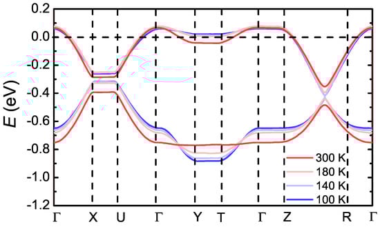
Figure A2.
Band structure of (TMTTF)SbF in a temperature range from 300 K (dark red) to 100 K (dark blue) on the selected k-path: .
Appendix A.2. Optical Spectra
Since optical spectra of the Fabre salts have not yet been theoretically investigated to our best knowledge, we have performed DFT calculations to derive the optical constants for all three crystallographic axes. While the excitation spectra were calculated for an evenly spaced grid of 132 k-points, the same functional, smearing factor, and cutoff energies were used as reported in the previous paragraph. The interband transitions were folded with a Lorentz function with a width of 100 meV, in contrast, for the Drude a width of 10 meV was assumed.
Figure A3 displays the optical conductivity of (TMTTF)SbF in a frequency range between 1000 cm and 30,000 cm for temperatures between 300 K and 100 K. Below 5000 cm, the a-direction is dominated by a Drude component (marked by I). Note, the deviations from the experimentally observed spectra (Figure 3b). can be explained by electronic correlations—driving the system insulating—and emv-coupled vibrational features, not taken in to account here. While the Drude term is less pronounced in the b-direction, the c-direction does not reveal any Drude component and drops to zero as . The ratio of the optical dc resistivity is :::10:6500 which agrees well with the result of the transport measurements [10].
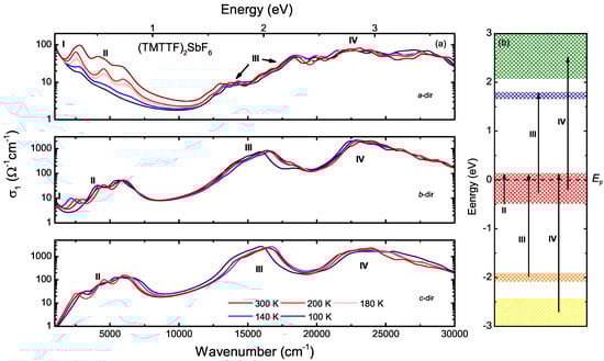
Figure A3.
(a) Calculated optical conductivity of (TMTTF)SbF between and 100 K in a frequency range from 1000 cm to 30,000 cm for the a-, b-, and c-direction; (b) Schematic diagram of the transitions between the occupied and unoccupied bands which are labeled by the corresponding markers from the optical conductivity spectra in (a).
On top of the Drude feature several resonances II are superimposed which can also be found in the c-direction. These are excitations from the completely occupied band near the Fermi energy into the empty states above , being the strongest for the b- and c-direction. Since no correlation effects are taken into account in the DFT calculations, the mid-infrared II band is not determined correctly. In the case of electron-electron correlations, the spectral weight of the Drude component is transferred to the mid-infrared band, leading to an enhancement of it. The weaker and broader interband transitions (III) occur for the a-, b-, and c-direction between 12,000 cm and 20,000 cm. They can be attributed to the excitation from the half-occupied band to the lowest unoccupied band LUMO, which is located 1.7 eV above , as depicted in Figure A3b. Moreover, also the excitations from the fully occupied bands −2 eV below to the half-filled band contributes to this feature. The smeared feature IV resides above 20,000 cm and can be assigned to the transition from the HOMO to the unoccupied bands located at 2 eV in the band structure and from the occupied bands being located −2.5 eV below to the half-occupied band at .
By comparing the intensity of the features III and IV for the various directions, it is evident that the bands in the stacking direction are by a factor of 10 less intense. This is because these transitions are caused by intramolecular electronic transitions of the cation molecule TMTTF, whose dipole moment is along the molecular axis. From the crystal structure it can be deduced that the long molecular axis of the TMTTF molecules is mainly oriented along the c-axis. For instance, the transition from the occupied band at the Fermi energy to the band at 1.7 eV corresponds to the transition from the HOMO of the TMTTF molecule in the LUMO. The excitation energy of this transition decreases with increasing molecule size.
Besides the overall shape of the spectra and the assignment of the features it is very interesting to track the temperature evolution of the spectra and compare it to the experimental measurements. The II band reveals the largest temperature dependence. In the a-direction, its intensity decreases on cooling and vanishes in the Drude component, while for the b- and c-direction it only shifts to lower and to higher frequencies, respectively. In addition, also the III- and IV-bands exhibit a temperature-dependent modification. Therefore, also the electronic excitations into higher energy levels can be used to track thermal effects. This is also true for phase transitions which are accompanied by a strong transfer of spectral weight.
References
- Ishiguro, T.; Yamaji, K.; Saito, G. Organic Superconductors, 2nd ed.; Springer: Berlin, Germany, 1998. [Google Scholar]
- Lebed, A. (Ed.) The Physics of Organic Superconductors and Conductors; Springer Series in Materials Science; Springer: Berlin, Germany, 2008; Volume 110. [Google Scholar]
- Dressel, M. Spin-charge separation in quasi one-dimensional organic conductors. Naturwissenschaften 2003, 90, 337–344. [Google Scholar] [CrossRef] [PubMed]
- Dressel, M. Ordering phenomena in quasi-one-dimensional organic Conductors. Naturwissenschaften 2007, 94, 527–541. [Google Scholar] [CrossRef] [PubMed]
- Dumm, M.; Abaker, M.; Dressel, M. Mid-infrared response of charge-ordered quasi-1D organic conductors (TMTTF)2X. J. Phys. IV 2005, 131, 55–58. [Google Scholar] [CrossRef]
- Knoblauch, T.; Dressel, M. Charge disproportionation in (TMTTF)2X (X= PF6, AsF6 and SbF6) investigated by infrared spectroscopy. Phys. Status Solidi (C) 2012, 9, 1158–1160. [Google Scholar] [CrossRef]
- Dressel, M.; Dumm, M.; Knoblauch, T.; Masino, M. Comprehensive Optical Investigations of Charge Order in Organic Chain Compounds (TMTTF)2X. Crystals 2012, 2, 528–578. [Google Scholar] [CrossRef]
- Voloshenko, I.; Herter, M.; Beyer, R.; Pustogow, A.; Dressel, M. Pressure-dependent optical investigations of Fabre salts in the charge-ordered state. J. Phys. Condens. Matter 2017, 29, 115601. [Google Scholar] [CrossRef] [PubMed]
- Świetlik, R.; Barszcz, B.; Pustogow, A.; Dressel, M. Raman spectroscopy evidence of domain walls in the organic electronic ferroelectrics (TMTTF)2X (X = SbF6, AsF6, PF6). Phys. Rev. B 2017, 95, 085205. [Google Scholar] [CrossRef]
- Köhler, B.; Rose, E.; Dumm, M.; Untereiner, G.; Dressel, M. Comprehensive transport study of anisotropy and ordering phenomena in quasi-one-dimensional (TMTTF)2X salts (X = PF6, AsF6, SbF6, BF4, ClO4, ReO4). Phys. Rev. B 2011, 84, 035124. [Google Scholar] [CrossRef]
- Pouget, J.P. Structural Aspects of the Bechgaard and Fabre Salts: An Update. Crystals 2012, 2, 466–520. [Google Scholar] [CrossRef]
- Pustogow, A.; Peterseim, T.; Kolatschek, S.; Engel, L.; Dressel, M. Electronic correlations versus lattice interactions: Interplay of charge and anion orders in (TMTTF)2X. Phys. Rev. B 2016, 94, 195125. [Google Scholar] [CrossRef]
- Rose, E.; Loose, C.; Kortus, J.; Pashkin, A.; Kuntscher, C.A.; Ebbinghaus, S.G.; Hanfland, M.; Lissner, F.; Schleid, T.; Dressel, M. Pressure-dependent structural and electronic properties of quasi-one-dimensional (TMTTF)2PF6. J. Phys. Condens. Matter 2013, 25, 014006. [Google Scholar] [CrossRef] [PubMed]
- Jacko, A.C.; Feldner, H.; Rose, E.; Lissner, F.; Dressel, M.; Valentí, R.; Jeschke, H.O. Electronic properties of Fabre charge-transfer salts under various temperature and pressure conditions. Phys. Rev. B 2013, 87, 155139. [Google Scholar] [CrossRef]
- Medjanik, K.; de Souza, M.; Kutnyakhov, D.; Gloskovskii, A.; Müller, J.; Lang, M.; Pouget, J.P.; Foury-Leylekian, P.; Moradpour, A.; Elmers, H.J.; et al. Hard X-ray photoemission study of the Fabre salts (TMTTF)2X (X = SbF6 and PF6). Eur. Phys. J. B 2014, 87, 256. [Google Scholar] [CrossRef]
- Salameh, B.; Yasin, S.; Dumm, M.; Untereiner, G.; Montgomery, L.; Dressel, M. Spin dynamics of the organic linear chain compounds (TMTTF)2X (X = SbF6, AsF6, BF4, ReO4, and SCN). Phys. Rev. B 2011, 83, 205126. [Google Scholar] [CrossRef]
- Yasin, S.; Salameh, B.; Rose, E.; Dumm, M.; von Nidda, H.A.K.; Loidl, A.; Ozerov, M.; Untereiner, G.; Montgomery, L.; Dressel, M. Broken magnetic symmetry due to charge-order ferroelectricity discovered in (TMTTF)2X salts by multifrequency ESR. Phys. Rev. B 2012, 85, 144428. [Google Scholar] [CrossRef]
- Dressel, M.; Dumm, M.; Knoblauch, T.; Köhler, B.; Salameh, B.; Yasin, S. Charge Order Breaks Magnetic Symmetry in Molecular Quantum Spin Chains. Adv. Condens. Matter Phys. 2012, 2012, 398721. [Google Scholar] [CrossRef]
- Matsunaga, N.; Hirose, S.; Shimohara, N.; Satoh, T.; Isome, T.; Yamomoto, M.; Liu, Y.; Kawamoto, A.; Nomura, K. Charge ordering and antiferromagnetism in (TMTTF)2SbF6. Phys. Rev. B 2013, 87, 144415. [Google Scholar] [CrossRef]
- Bertaina, S.; Dutoit, C.E.; Van Tol, J.; Dressel, M.; Barbara, B.; Stepanov, A. Rabi oscillations of pinned solitons in spin chains: A route to quantum computation and communication. Phys. Rev. B 2014, 90, 060404. [Google Scholar] [CrossRef]
- Dutoit, C.E.; Bertaina, S.; Orio, M.; Dressel, M.; Stepanov, A. Charge-ordering induces magnetic axes rotation in organic materials (TMTTF)2X (with X = SbF6, AsF6, and PF6). Low Temp. Phys. 2015, 41, 942–944. [Google Scholar] [CrossRef]
- Dressel, M.; Grüner, G.; Pouget, J.; Breining, A.; Schweitzer, D. Field and frequency dependent transport in the two-dimensional organic conductor α-(BEDT-TTF)2I3. J. Phys. I 1994, 4, 579–594. [Google Scholar] [CrossRef]
- Dressel, M.; Grüner, G.; Pouget, J.; Breining, A.; Schweitzer, D. Non-linear transport in α-(BEDT-TTF)2I3. Synth. Met. 1995, 70, 929–930. [Google Scholar] [CrossRef]
- Ivek, T.; Korin-Hamzić, B.; Milat, O.; Tomić, S.; Clauss, C.; Drichko, N.; Schweitzer, D.; Dressel, M. Collective Excitations in the Charge-Ordered Phase of α-(BEDT-TTF)2I3. Phys. Rev. Lett. 2010, 104, 206406. [Google Scholar] [CrossRef] [PubMed]
- Ivek, T.; Korin-Hamzić, B.; Milat, O.; Tomić, S.; Clauss, C.; Drichko, N.; Schweitzer, D.; Dressel, M. Electrodynamic response of the charge ordering phase: Dielectric and optical studies of α-(BEDT-TTF)2I3. Phys. Rev. B 2011, 83, 165128. [Google Scholar] [CrossRef]
- Ito, A.; Nakamura, Y.; Nakamura, A.; Kishida, H. Measurement of the Nonlinear Conducting States of α-(BEDT-TTF)2I3 Using Electronic Raman Scattering. Phys. Rev. Lett. 2013, 111, 197801. [Google Scholar] [CrossRef] [PubMed]
- Itose, F.; Kawamoto, T.; Mori, T. Collective response to alternating current in the organic conductor a-(bis(ethylenedithio)tetrathiafulvalene)2I3. J. Appl. Phys. 2013, 113, 213702. [Google Scholar] [CrossRef]
- Peterseim, T.; Ivek, T.; Schweitzer, D.; Dressel, M. Electrically induced phase transition in α-(BEDT-TTF)2I3: Indications for Dirac-like hot charge carriers. Phys. Rev. B 2016, 93, 245133. [Google Scholar] [CrossRef]
- Tajima, N.; Fujisawa, J.I.; Naka, N.; Ishihara, T.; Kato, R.; Nishio, Y.; Kajita, K. Photo-induced insulator metal transition in an organic conductor α-(BEDT-TTF)2I3. J. Phys. Soc. Jpn. 2005, 74, 511–514. [Google Scholar] [CrossRef]
- Dearnaley, G.; Stoneham, A.M.; Morgan, D.V. Electrical phenomena in amorphous oxide films. Rep. Prog. Phys. 1970, 33, 1129–1191. [Google Scholar] [CrossRef]
- Mori, T.; Kawamoto, T.; Terasaki, I.; Kakiuchi, T.; Sawa, H. Nonlinear conductivity with an extremely small threshold electric field in the organic conductor (TSM-TTP)(I3)5/3. Phys. Rev. B 2007, 75, 235103. [Google Scholar] [CrossRef]
- Sze, S.M.; Ng, K.K. (Eds.) Physics of Semiconductor Devices, 3rd ed.; Wiley-Interscience: Hoboken, NJ, USA, 2007. [Google Scholar]
- Yu, P.; Cardona, M. (Eds.) Fundamentals of Semiconductors: Physics and Material Properties, 4th ed.; Graduate Texts in Physics; Springer: Berlin, Germany, 2010. [Google Scholar]
- Potember, R.S.; Poehler, T.O.; Cowan, D.O. Electrical switching and memory phenomena in Cu-TCNQ thin films. Appl. Phys. Lett. 1979, 34, 405–407. [Google Scholar] [CrossRef]
- Tokura, Y.; Okamoto, H.; Koda, T.; Mitani, T.; Saito, G. Nonlinear electric transport and switching phenomenon in the mixed-stack charge-transfer crystal tetrathiafulvalene-p-chloranil. Phys. Rev. B 1988, 38, 2215–2218. [Google Scholar] [CrossRef]
- Kumai, R.; Okimoto, Y.; Tokura, Y. Current-induced insulator-metal transition and pattern formation in an organic charge-transfer complex. Science 1999, 284, 1645–1647. [Google Scholar] [CrossRef]
- Inagaki, K.; Terasaki, I.; Mori, H.; Mori, T. Large Dielectric Constant and Giant Nonlinear Conduction in the Organic Conductor θ-(BEDT-TTF)2CsZn(SCN)4. J. Phys. Soc. Jpn. 2004, 73, 3364–3369. [Google Scholar] [CrossRef]
- Sawano, F.; Terasaki, I.; Mori, H.; Mori, T.; Watanabe, M.; Ikeda, N.; Nogami, Y.; Noda, Y. An organic thyristor. Nature 2005, 437, 522–524. [Google Scholar] [CrossRef] [PubMed]
- Dumm, M.; Loidl, A.; Fravel, B.W.; Starkey, K.P.; Montgomery, L.K.; Dressel, M. Electron spin resonance studies on the organic linear-chain compounds (TMTCF)2X (C = S, Se; X = PF6, AsF6, ClO4, Br). Phys. Rev. B 2000, 61, 511–521. [Google Scholar] [CrossRef]
- Monceau, P.; Nad, F.Y.; Brazovskii, S. Ferroelectric Mott-Hubbard Phase of Organic (TMTTF)2X Conductors. Phys. Rev. Lett. 2001, 86, 4080–4083. [Google Scholar] [CrossRef] [PubMed]
- Fujiyama, S.; Nakamura, T. Redistribution of Electronic Charges in Spin-Peierls State in (TMTTF)2AsF6 Observed by 13C NMR. J. Phys. Soc. Jpn. 2006, 75, 014705. [Google Scholar] [CrossRef]
- Oka, Y.; Matsunaga, N.; Nomura, K.; Kawamoto, A.; Yamamoto, K.; Yakushi, K. Charge Order in (TMTTF)2TaF6 by Infrared Spectroscopy. J. Phys. Soc. Jpn. 2015, 84, 114709. [Google Scholar] [CrossRef]
- Pashkin, A.; Dressel, M.; Kuntscher, C.A. Pressure-Induced Deconfinement of the Charge Transport in the Quasi-One-Dimensional Mott Insulator (TMTTF)2AsF6. Phys. Rev. B 2006, 74, 165118. [Google Scholar] [CrossRef]
- Pashkin, A.; Dressel, M.; Hanfland, M.; Kuntscher, C.A. Deconfinement transition and dimensional crossover in the Bechgaard-Fabre salts: Pressure- and temperature-dependent optical investigations. Phys. Rev. B 2010, 81, 125109. [Google Scholar] [CrossRef]
- Ivek, T.; Kovačević, I.; Pinterić, M.; Korin-Hamzić, B.; Tomić, S.; Knoblauch, T.; Schweitzer, D.; Dressel, M. Cooperative dynamics in charge-ordered state of α-(BEDT-TTF)2I3. Phys. Rev. B 2012, 86, 245125. [Google Scholar] [CrossRef]
- Joshi, N.V. Photoconductivity: Art, Science and Technology; Marcel Dekker: New York, NY, USA; Basel, Switzerland, 1990. [Google Scholar]
- Peterseim, T.; Dressel, M.; Dietrich, M.; Polity, A. Optical properties of VO2 films at the phase transition: Influence of substrate and electronic correlations. J. Appl. Phys. 2016, 120, 075102. [Google Scholar] [CrossRef]
- Peterseim, T.; Dressel, M. Molecular Dynamics at Electrical- and Optical-Driven Phase Transitions: Time-Resolved Infrared Studies Using Fourier-Transform Spectrometers. J. Infrared Millim. Terahertz Waves 2017, 38, 104–123. [Google Scholar] [CrossRef]
- De Souza, M.; Foury-Leylekian, P.; Moradpour, A.; Pouget, J.P.; Lang, M. Evidence for Lattice Effects at the Charge-Ordering Transition in (TMTTF)2X. Phys. Rev. Lett. 2008, 101, 216403. [Google Scholar] [CrossRef] [PubMed]
- Monceau, P. Electronic crystals: An experimental overview. Adv. Phys. 2012, 61, 325–581. [Google Scholar]
- Jérome, D.; Schulz, H.J. Organic Conductors and Superconductors. Adv. Phys. 1982, 31, 299–490. [Google Scholar] [CrossRef]
- Kagoshima, S.; Nagasawa, H.; Sambongi, T. One-Dimensional Conductors; Springer: Berlin, Germany, 1988. [Google Scholar]
- Organic Conductors; Farges, J.P. (Ed.) Marcel Dekker: New York, NY, USA, 1994. [Google Scholar]
- Devreese, J.T.; Evrand, R.P.; von Doren, V.E. (Eds.) Highly Conducting One-Dimensional Solids; Plenum Press: New York, NY, USA; London, UK, 1979. [Google Scholar]
- Tanaka, S.; Uchinokura, K. (Eds.) Physics and Chemistry of Quasi One-Dimensional Conductors; Physica B; North-Holland: Amsterdam, The Ntherlands, 1986; Volume 143. [Google Scholar]
- Jérome, D.; Caron, L. (Eds.) Low-Dimensional Conductors and Superconductors; Nato ASI, Series B: Physics; Plenum Press: New York, NY, USA; London, UK, 1987; Volume 155. [Google Scholar]
- Delhaes, P.; Drillon, M. (Eds.) Organic and Inorganic Low-Dimensional Crystalline Materials; Nato ASI, Series B: Physics; Plenum Press: New York, NY, USA; London, UK, 1987; Volume 168. [Google Scholar]
- Saito, G.; Kagoshima, S. (Eds.) The Physics and Chemistry of Organic Superconductors; Springer Proceedings in Physics; Springer: Berlin, Germany, 1990; Volume 51. [Google Scholar]
- Bernier, P.; Lafrant, S.; Bidan, G. (Eds.) Advances in Synthetic Metals: Twenty Years of Progress in Science and Technology; Elsevier: Amsterdam, The Ntherlands, 1999. [Google Scholar]
- Grüner, G. The dynamics of charge-density waves. Rev. Mod. Phys. 1988, 60, 1129–1181. [Google Scholar]
- Dressel, M.; Drichko, N.; Kaiser, S. Collective charge-order excitations. Physica C 2010, 470, S589–S591. [Google Scholar] [CrossRef]
- Iimori, T.; Naito, T.; Ohta, N. Photoinduced Phase Transition in the Organic Conductor α-(BEDT-TTF)2I3 at Temperatures near the Metal–Insulator Phase Transition. Chem. Lett. 2007, 36, 536. [Google Scholar] [CrossRef]
- Iimori, T.; Naito, T.; Ohta, N. Photoresponse of electrical conductivity in an organic superconductor investigated by time-resolved resistance measurements. Physica B 2010, 405, S347–S349. [Google Scholar] [CrossRef]
- Tsutsumi, J.; Yamada, T.; Matsui, H.; Haas, S.; Hasegawa, T. Competition between Charge-Transfer Exciton Dissociation and Direct Photocarrier Generation in Molecular Donor-Acceptor Compounds. Phys. Rev. Lett. 2010, 105, 226601. [Google Scholar] [CrossRef] [PubMed]
- Iimori, T.; Ohta, N. Tuning of Electrical Conductivity by Photoirradiation and Electric Fields. J. Phys. Chem. C 2014, 118, 7251–7260. [Google Scholar] [CrossRef]
- Iwasa, Y.; Koda, T.; Tokura, Y.; Koshihara, S.; Iwasawa, N.; Saito, G. Switching effect in organic charge transfer complex crystals. Appl. Phys. Lett. 1989, 55, 2111–2113. [Google Scholar] [CrossRef]
- Iwasa, Y.; Koda, T.; Koshihara, S.; Tokura, Y.; Iwasawa, N.; Saito, G. Intrinsic negative-resistance effect in mixed-stack charge-transfer crystals. Phys. Rev. B 1989, 39, 10441–10444. [Google Scholar] [CrossRef]
- Ozawa, T.; Tamura, K.; Bando, Y.; Kawamoto, T.; Mori, T.; Terasaki, I. Giant nonlinear conductivity in an organic conductor with a sharp metal-insulator transition: β″-(BEDT-TTF)3(HSO4)2. Phys. Rev. B 2009, 80, 155106. [Google Scholar] [CrossRef]
- Mori, T.; Ozawa, T.; Bando, Y.; Kawamoto, T.; Niizeki, S.; Mori, H.; Terasaki, I. Nonlinear dynamics of conduction electrons in organic conductors. Phys. Rev. B 2009, 79, 115108. [Google Scholar] [CrossRef]
- Dressel, M.; Peterseim, T. Infrared Investigations of the Neutral-Ionic Phase Transition in TTF-CA and Its Dynamics. Crystals 2017, 7, 17. [Google Scholar] [CrossRef]
- Drichko, N.; Hackl, R.; Schlueter, J. Localized states in the Mott insulator κ-(BEDT-TTF)2Cu[N(CN)2]Cl as probed by photoluminescence. Phys. Rev. B 2013, 88, 115109. [Google Scholar] [CrossRef]
- Nasu, K. (Ed.) Relaxations of Excited States and Photo-Induced Structural Phase Transitions. Springer Series in Solid State Science. In Proceedings of the 19th Taniguchi Sumposium, Kashikojima, Japan, 18–23 July 1996; Springer: Berlin, Germany, 1997; Volume 124. [Google Scholar]
- Peterseim, T.; Haremski, P.; Dressel, M. Random-walk annihilation process of photo-induced neutral-ionic domain walls in TTF-CA. Europhys. Lett. 2015, 109, 67003. [Google Scholar] [CrossRef]
- Kassing, R.; Kähler, E. Low-frequency current oscillations in high-resistivity, Au-doped silicon junctions with two Schottky contacts. Phys. Status Solidi (A) 1972, 12, 209–213. [Google Scholar] [CrossRef]
- Holonyak, N.; Bevacqua, S.F. Oscillations in semiconductors due to deep levels. Appl. Phys. Lett. 1963, 2, 71–73. [Google Scholar] [CrossRef]
- Kastrup, J.; Hey, R.; Ploog, K.H.; Grahn, H.T.; Bonilla, L.L.; Kindelan, M.; Moscoso, M.; Wacker, A.; Galán, J. Electrically tunable GHz oscillations in doped GaAs-AlAs superlattices. Phys. Rev. B 1997, 55, 2476–2488. [Google Scholar] [CrossRef]
- Hosoda, M.; Mimura, H.; Ohtani, N.; Tominaga, K.; Watanabe, T.; Fujiwara, K.; Grahn, H.T. Current self-oscillations in photoexcited type-II GaAs-AlAs superlattices. Appl. Phys. Lett. 1996, 69, 500–502. [Google Scholar] [CrossRef]
- Tomlinson, A.M.; Fox, A.M.; Cunningham, J.E.; Jan, W.Y. Photocurrent self-oscillations in a spatially direct GaAs/AlGaAs superlattice. Appl. Phys. Lett. 1999, 75, 2067–2069. [Google Scholar] [CrossRef]
- Mori, T.; Bando, Y.; Kawamoto, T.; Terasaki, I.; Takimiya, K.; Otsubo, T. Giant Nonlinear Conductivity and Spontaneous Current Oscillation in an Incommensurate Organic Superconductor. Phys. Rev. Lett. 2008, 100, 037001. [Google Scholar] [CrossRef] [PubMed]
- Tamura, K.; Ozawa, T.; Bando, Y.; Kawamoto, T.; Mori, T. Voltage oscillation associated with nonlinear conductivity in the organic conductor α-(BEDT-TTF)2I3. J. Appl. Phys. 2010, 107, 103716. [Google Scholar] [CrossRef]
- Wakita, H.; Ozawa, T.; Bando, Y.; Mori, T. Nonlinear Conductivity in Dicyanoquinonediimine Complexes. J. Phys. Soc. Jpn. 2010, 79, 094703. [Google Scholar] [CrossRef]
- Kishida, H.; Ito, T.; Ito, A.; Nakamura, A. Room-Temperature Current Oscillation Based on Negative Differential Resistance in a One-Dimensional Organic Charge-Transfer Complex. Appl. Phys. Express 2011, 4, 031601. [Google Scholar] [CrossRef]
- Ivek, T.; Čulo, M.; Kuveždić, M.; Korin-Hamzić, B.; Tutiš, E.; Basletić, M.; Mihaljević, B.; Tafra, E.; Löhle, A.; Dressel, M.; et al. Semimetallic and charge-ordered α-(BEDT-TTF)2I3: On the role of disorder in dc transport and dielectric properties. Phys. Rev. B 2017, 96, 123456. [Google Scholar] [CrossRef]
- Lines, M.; Glass, A. (Eds.) Principles and Applications of Ferroelectrics and Related Materials; International Series of Monographs on Physics; Clarendon Press: Oxford, UK, 1977. [Google Scholar]
- Glass, A.M.; Abrams, R.L. Study of Piezoelectric Oscillations in Wideband Pyroelectric LiTaO3 Detectors. J. Appl. Phys. 1970, 41, 4455–4459. [Google Scholar] [CrossRef]
- Glass, A.; Auston, D. Excited state dipole moments of impurities in polar crystals. Opt. Commun. 1972, 5, 45–49. [Google Scholar] [CrossRef]
- Glass, A.M.; Auston, D.H. Excited state dipole moments of impurities in pyroelectric crystals and their applications. Ferroelectrics 1974, 7, 187–189. [Google Scholar] [CrossRef]
- Tomic, S.; Dressel, M. Ferroelectricity in molecular solids: A review of electrodynamic properties. Rep. Prog. Phys. 2015, 78, 096501. [Google Scholar] [CrossRef] [PubMed]
- Ogawa, N.; Shiraga, A.; Kondo, R.; Kagoshima, S.; Miyano, K. Photocontrol of Dynamic Phase Transition in the Charge-Density Wave Material K0.3MoO3. Phys. Rev. Lett. 2001, 87, 256401. [Google Scholar] [CrossRef] [PubMed]
- Ogawa, N.; Miyano, K.; Brazovski, S. Optical excitation in the creep phase of plastic charge-density waves. Phys. Rev. B 2005, 71, 075118. [Google Scholar] [CrossRef]
- Tiedje, T.; Haering, R.; Jericho, M.; Roger, W.; Simpson, A. Temperature dependence of sound velocities in TTF-TCNQ. Solid State Commun. 1977, 23, 713–718. [Google Scholar] [CrossRef]
- Chaikin, P.; Tiedje, T.; Bloch, A. Sound velocity measurements on (TMTSF)2PF6. Solid State Commun. 1982, 41, 739–742. [Google Scholar] [CrossRef]
- Zherlitsyn, S.; Bruls, G.; Goltsev, A.; Alavi, B.; Dressel, M. Acoustical properties of (TMTSF)2PF6 in the spin-density-wave ground state. Phys. Rev. B 1999, 59, 13861–13871. [Google Scholar] [CrossRef]
- Giannozzi, P.; Baroni, S.; Bonini, N.; Calandra, M.; Car, R.; Cavazzoni, C.; Ceresoli, D.; Chiarotti, G.L.; Cococcioni, M.; Dabo, I.; et al. QUANTUM ESPRESSO: A modular and open-source software project for quantum simulations of materials. J. Phys. Condens. Matter 2009, 21, 395502. [Google Scholar] [CrossRef]
- Galigne, J.L.; Liautard, B.; Peytavin, S.; Brun, G.; Fabre, J.M.; Torreiles, E.; Giral, L. Etude Structurale Du Bromure de Tetramethyltetrathiofulvalene, (TMTTF)2Br. Acta Crystallogr. B 1978, 34, 620–624. [Google Scholar] [CrossRef]
© 2017 by the authors. Licensee MDPI, Basel, Switzerland. This article is an open access article distributed under the terms and conditions of the Creative Commons Attribution (CC BY) license (http://creativecommons.org/licenses/by/4.0/).