Abstract
Light sources tend to affect images captured in any automatic optical inspection (AOI) system. In this study, the effectiveness of metal-halide lamps, quartz-halogen lamps, and LEDs as the light sources in AOI systems for the detection of the third and fourth layers electrodes of thin-film-transistor liquid crystal displays (TFT-LCDs) is examined experimentally. The results show that the performance of LEDs is generally comparable or better than that of metal-halide and quartz-halogen lamps. The best optical performance is by the blue LED due to its spectrum compatibility with the time-delay-integration charged-coupled device (TDI CCD) sensor and its better spatial resolution. The images revealed by the blue LED are sharper and more distinctive. Since current LEDs are more energy efficient and environmentally friendly, using LEDs as the light source for AOI is very beneficial. As the blue LED performs the best, it should be adopted for AOI using TDI CCD sensors.
1. Introduction
In the market of flat panel displays, especially the larger sizes, thin-film-transistor liquid crystal displays (TFT-LCDs) are currently the dominant product. With the progress in manufacturing, the product is moving from the high-definition television (1920 × 1080 pixels) of about 6 million subpixels toward the ultra-high resolution television of 10 million pixels and beyond. The latter has wide view illumination, sharp contrast, fast response, lower power consumption, and minimum radiation [1,2]. The wide view illumination coupled to the ultra-high definition (UHD) of 4K (3840*2160) is expected to move to 8K (7680*4320), 16K (15,360*8640), and 32K (30,720*17,280) [3] as the technology advances. The TFT of LCDs investigated in this study is fabricated by the back-channel etching process. It consists of five layers as (1) gate metal, (2) TFT layer (gate dielectric/channel/n+), (3) source/drain (S/D) metal, (4) silicon nitride (SiNx) passivation layer, and (5) indium tin oxide (ITO) pixel electrode. Additionally, there is low resistance gate metallisation using aluminium or copper, capped by chromium (Cr) on the third layer [4,5,6]. They are typically deposited either by physical vapour deposition (PVD) or by plasma enhanced chemical vapour deposition (PECVD).
Among these five layers, the third and fourth layers control both the light switching function of the liquid crystal and the frame rate of the LCD. Thus, in this study, the quality of these two layers is examined by an in-line automatic optical inspection (AOI) system for which the light source plays a key part. Presently in the display industry, the main light sources for AOI are the metal-halide and quartz-halogen lamps. Metal-halide lamps generally have a lifespan values range from of 6000 to 15,000 h [7,8] and provide good colour rendering due to their high-intensity discharge (HID) characteristic. However, their functioning requires 250 Wp. They are also very sensitive to voltage levels. If the operation voltage was lower than 220 V, the output light will decay immediately and may even shutdown completely. Moreover, they need warmup times (averaging a couple minutes) for stable operation. In addition, the lighting intensity tends to vary from lamp to lamp. In contrast, quartz-halogen lamps radiate significant amounts of heat with a lifespan of about 2000 h and cost more. Furthermore, the halogen elements are harmful to both human health and to the environment, and do not conform to the Waste Electrical and Electronic Equipment Directive (WEEE) and Restriction of Hazardous Substances [9]. Hence, with the growing concerns of global warming and its impact on the environment, a light source that is environmentally friendly and offers energy savings is of interest, and light emitting diodes (LEDs) are a potential alternative.
LEDs are solid state semiconductor devices of p-n junction diodes. They are highly energy efficient with an attainable lumen per watt of ~200 (lm/W), which is much better than both HID and halogen lamps. Furthermore, they contain no halogen elements. Namely, they are both energy efficient and environmentally friendly. Chulkov et al. [10] applied both LEDs and halogen light sources to inspect metallic materials which could lead to corrosion by active thermal waves. The effect of paint-and-lacquer coating colour on the heating efficiency using these light sources was analysed. The possibility of using LED thermal stimulation in portable flaw detectors was then described. The results showed that the LED performs well and is cost effective and suitable for AOI. Thus, LEDs look promising for AOI applications. Hence, in this study, the suitability of using LEDs in AOI of TFTs is examined by comparing their performance with commonly adopted light sources in the TFT-LCD industry.
2. System Architecture
The experiments were conducted in a class 1000 clean-room at 25 °C using tailor-made samples of the 6th generation glass panel with TFT electrode pixels. For the inspection of the third and fourth layers of TFT structures by image scanning, a line-scan of time-delay-integration (TDI) of a charge-coupled device (CCD) was employed. The TDI CCD can capture more images with the pixels in synchronization of the moving object, thus allowing the data packet to continuously track the motion of the object [11,12].
A commercial off-the-shelf HS 8 K TDI CCD (Piranha HS 8 K 68 kHz, TELEDYNE DALSA) was adopted for this task. Its photoelectric sensors can scan the images in hundreds of thousands of lines per second at very high speed and can also operate under low light levels and slower speed conditions if necessary. The optical resolution of the sensor is 1 μm; the wavelength is from ultra-ultraviolet (UV) to infrared (IR) with the maximum quantum efficiency of 38% occurring at the wavelength of ~520 nm. In other words, this device captures multiple exposures of the moving object to achieve higher responsivity. Figure 1 depicts a schematic diagram of the measurement setup. A computer-controlled gantry was installed to scan the samples that were held with a non-reflective film to avoid light interference. The main components of the scan model include the TDI CCD, the light source, a focusing lens, a fiber, a spectrometer, and a host computer. Reflected lights from the sample were captured by the CCD and fed to the automatic data acquisition program in the host computer for data analysis.
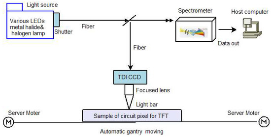
Figure 1.
Scanning mode of AOI architecture.
For the purpose of comparison, the light sources employed included a 250 Wp metal-halide lamp (PCS-UMX250, COLDSPOT, NPI), a 250 Wp quartz-halogen lamp (MHF-KFB100LR, MORITEX) and monochromatic LEDs. Since the light spectra of metal-halide and quartz-halogen lamps are wide band (described in the next section), red, orange, yellow, green, and blue optical filters (see Figure 2 and Figure 3) were used to narrow the light spectrum range.
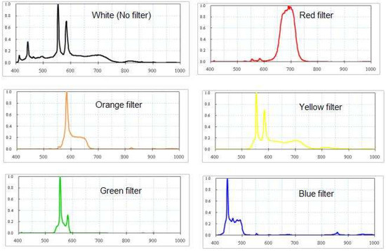
Figure 2.
Spectrum distribution of metal-halide light source.
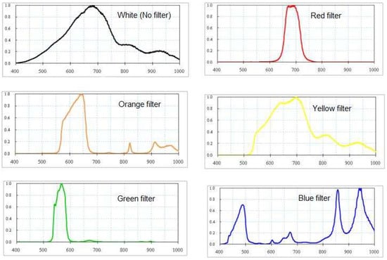
Figure 3.
Spectrum distributions of quartz-halogen light sources.
The characteristics of these filters are tabulated in Table 1 for reference. In contrast, as shown in Figure 4, the spectra of the applied LEDs were monochromatic, that is, red, green, and blue with wavelengths of 640 nm, 525 nm, and 460 nm, respectively; no filters were needed. They are InGaN-based high-brightness LEDs, driven by a forward maximum current of 27 A and provide 5500 lumens at 90 Wp.

Table 1.
Characteristics of the optical filters in the light source.
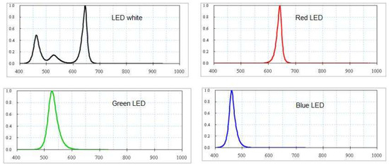
Figure 4.
Spectrum distribution of LED light source.
3. Results and Discussion
The spectra of the light sources, including those being filtered by the individual colour filter, were measured by a commercial off-the-shelf spectrometer (FDSP with spectral range 380–1050 nm, ETA-Optik). It is clear in Figure 2 that the spectrum of the white light of the metal-halide lamp has three sharp peaks with wavelengths at 440 nm, 570 nm, and 590 nm respectively, in addition to being wide band. Hence, after colour filtering, the wavelengths of the metal-halide lamp are 680 nm, 580 nm, 555 nm, 550 nm, and 445 nm for red, orange, yellow, green, and blue filters respectively. On the other hand, the quartz-halogen lamp of Figure 3, the spectrum is more widely distributed than that of metal-halide lamp of Figure 2. Whereas, the peaks after filtering by the red, orange, yellow, green, and blue filters occur at 690 nm, 640 nm, 555 nm (above), 560 nm, and 450 nm respectively. As these filters were designed following the Gaussian transmission curve [13,14] to emulate the narrow spectral distribution of monochromatic LEDs, the filtered spectrum distributions conform to the filter specifications listed in Table 1. That is, they have a relatively focused wavelength to improve the image quality. However, for the quartz-halogen lamp, a considerable amount of noise still exists for those filtered by the red, yellow, and blue filters, especially the blue colour. In contrast, the red, green, and blue LEDs as Figure 4, the peaks occur at wavelength of 660 nm, 530 nm, and 460 nm respectively, which are close to the maximum spectral response of the TDI CCD in the range of 460 nm to 580 nm. The result demonstrates the sharpness of the focused wavelength of the monochrome LED without noise.
Typical optical images of the third and fourth layers are shown in Figure 5 and Figure 6, respectively. Figure 5 illustrates the optical images obtained by using various light sources for the electrodes of the third layer source/drain (S/D) regions. The red light of both the filtered metal-halide lamp and the filtered quartz-halogen lamp results in blurred images. This is due to the spectrum is far from the maximum spectral response of the TDI CCD which is in the range of 460 nm to 580 nm. In contrast, the performance of the green light of both the filtered metal-halide lamp and the filtered quartz-halogen lamp is almost same as that of the green LED due to the similar spectrum among them. However, none of the green light gives the detailed metal traces exhibited by the blue light. For the blue light, the performance of the filtered metal-halide lamp is similar to that of the LED because of their narrow spectrum and the closeness to the maximum sensitivity of the TDI CCD. Whereas, the image quality of the blue light of the filtered quartz-halogen lamp is very poor due to its non-uniform and jagged spectrum. Hence, in terms of image quality of the third layer, the performance of the filtered metal-halide lamp is similar to that of the corresponding LED. However, the metal-halide lamp is relatively expensive, is very sensitive to the applied voltage, and its lighting intensity varies from lamp to lamp, in addition to its non-environmentally friendly characteristic. Thus, the blue LED is the most suitable light source for the third layer electrodes (marked by the tick symbol in Figure 5).
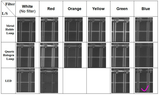
Figure 5.
The third layer circuit pixel by various lamps for optical detection in TFT.
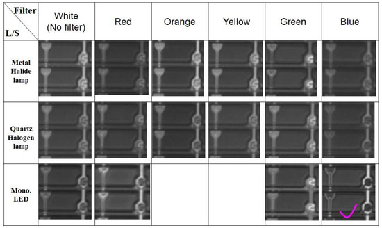
Figure 6.
The fourth layer circuit pixel by various lamps for optical detection in TFT.
Figure 6 displays the optical images for the fourth layer TFT electrodes obtained by using various light sources. Overall comparison of the results show that the performance of the metal-halide lamp, the quartz-halogen lamp, and the LED is approximately the same, except that of the blue LED. The blue LED outperforms all of the other light sources. That is, the blue LED gives the clearest image (marked by a tick symbol) due to its short wavelength and better spatial resolution.
From the spectrum distribution shown in Figure 2, it is clear that the blue light of the filtered metal-halide lamp has a relatively clear peak at around 440 nm. However, it also contains wavelengths from 440 nm to 500 nm with a relatively constant proportion of about 25%. Hence, its performance is close to that of the blue LED for the third layer electrodes. But its performance for the fourth layer deteriorates due to scattering of the SiNx passivation.
The images shown in Figure 5 and Figure 6 indicate that the blue LED gives the best images for the third and fourth layer electrodes. Moreover, the image quality depends on both monochromatic and wavelength of the light source, not just either of them. Thus, in both Figure 5 and Figure 6, no images are presented for the orange and yellow LEDs because they are not readily available. And more importantly they are not monochromatic.
Wagatsuma [15] mentioned that the emitted optical spectrum of chromium illuminated by an argon glow discharge plasma is in the wavelength range of 200–440 nm [15]. Thus, the blue LED responds well to Cr to trigger the TDI CCD, and results in a better image than other light sources. Recently, the panel pixels with low-temperature polysilicon used for in-plane switching LCDs and organic LEDs have been pushed to very small dimensions. Therefore, a shorter wavelength for AOI detection is essential to the shrinking electrode dimensions of high definition LCD panels which require better spatial resolution for detection. In contrast, the image by the red LED light is the poorest among the three LED light colours because its wavelength is farther from the range of 460 nm to 580 nm of the HS 8K TDI CCD. In other words, compatibility between the sensor and the light source is critical to the success of an AOI system, in addition to spatial resolution. As a further illustration of the best performance of the blue LED, Figure 7 shows the images for the source and drain of the third layer and the contact passivation of the fourth layer when illuminated by LEDs. The performance in descending order are blue LED> green LED > red LED, consistent with the above results. In other words, the blue LED gives the clearest distinct images of sharp boundaries. Hence, by combining the results of the third and fourth layer, the blue LED has the best performance.
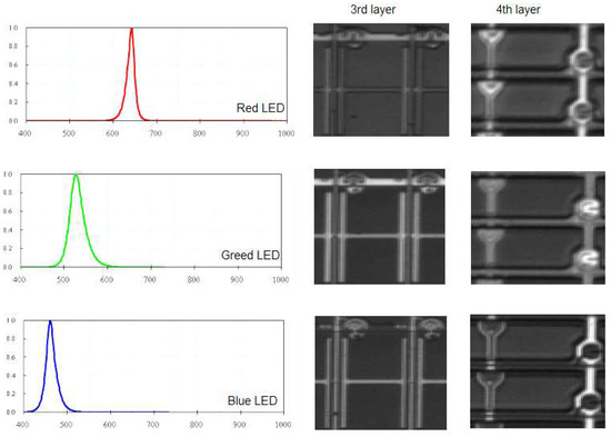
Figure 7.
Comparison of third and fourth layer electrode images in TFT by LEDs.
Moreover, the present monochromic LEDs consume 90 Wp, which is about 36% of 250 Wp of both quartz-halogen and metal-halide lamps. Furthermore, the LEDs typically have a lifespan of 50,000 h, much longer than 2000 h of quartz-halogen lamps and 6000 h of metal-halide lamps. In other words, the cost-per-performance of the blue LED is superior to other light sources examined in this study.
4. Conclusions
This study experimentally investigates the effectiveness of various light sources on scanning the electrode pixels of TFTs using TDI CCD. The results show that blue LEDs provide the clearest images of both the third and fourth layer electrodes. Hence, it is the most suitable light source because of its spectrum compatibility with the TDI CCD system and better spatial resolution due to it short wavelength. The cost-per-performance provided by the blue LED is superior compared to other light sources typically used in such studies. Since modern monochromic LEDs consume 90 Wp, which is ~36% of the 250 Wp required for both quartz-halogen lamp and metal-halide lamp, LEDs are clearly more energy efficient. Together with the relatively long life span and ecological friendliness, LEDs are viable light sources for AOI. This is especially true for the blue LED for its spectrum compatibility with the TDI CCD sensor and its better spatial resolution. In other words, it should be adopted in AOI for both energy and performance considerations.
Author Contributions
Data curation, F.M.T.; Formal analysis, F.M.T.; Methodology, F.M.T.; Validation, J.H.C.; Writing—original draft, F.M.T.; Writing—review & editing, F.M.T. and J.H.C.
Funding
This research received no external funding
Conflicts of Interest
The authors declare no conflict of interest
References
- Liu, S.; Wang, D.; Yang, Z.K.; Feng, X.; Sun, X.; Qiu, Y.; Dong, X. Key technology trends analysis of TFT-LCD. Chin. J. Liq. Cryst. Disp. 2018, 33, 457–463. [Google Scholar]
- Li, X.H.; Bao, J.P.; Xu, B.; Fan, H.Y. Improvement research of TFT-LCD module black uniformity. Chin. J. Liq. Cryst. Disp. 2018, 33, 271–276. [Google Scholar]
- Tzu, F.M.; Chou, J.H. Non-uniformity evaluation of flat panel display by automatic optical detection. In Proceedings of the 2016 11th International Microsystems, Packaging, Assembly and Circuits Technology Conference (IMPACT), Taipei, Taiwan, 26–28 October 2016; pp. 168–171. [Google Scholar]
- Hu, S.; Fang, Z.; Ning, H.; Tao, R.; Liu, X.; Zeng, Y.; Yao, R.; Huang, F.; Li, Z.; Xu, M.; et al. Effect of Post Treatment For Cu-Cr Source/Drain Electrodes on a-IGZO TFTs. Materials 2016, 9, 623. [Google Scholar] [CrossRef] [PubMed]
- Lee, C.H.; Sazonov, A.; Nathan, A. High hole and electron mobilities in nanocrystalline silicon thin-film transistors. J. Non Cryst. Solids 2006, 352, 1732–1736. [Google Scholar] [CrossRef]
- Powell, M.J.; Glasse, C.; Curran, J.E.; Hughes, J.R.; French, I.D.; Martin, B.F. A fully self-aligned amorphous silicon TFT technology for large area image sensors and active-matrix displays. In A Fully Self-Aligned Amorphous Silicon TFT Technology for Large Area Image Sensors and Active-Matrix Displays; Schropp, R., Branz, H.M., Hack., M., Shimizu, I., Wagner, S., Eds.; Amorphous and Microcrystalline Silicon Technology-1998; Cambridge University Press: Cambridge, UK, 2011. [Google Scholar]
- Grondzik, W.T.; Kwok, A.G.; Stein, B.; Reynolds, J.S. Mechanical and Electrical Equipment for Buildings; John Wiley & Sons Press: Hoboken, NJ, USA, 2014. [Google Scholar]
- Kumar, T.S.; Harikumar, G.; Halpeth, M.K. Light Right: A Practising Engineer’s Manual on Energy-Efficient Lighting; TERI Press: New Delhi, India, 2004; pp. 19–20. [Google Scholar]
- Groß, R.; Bunke, D.; Gensch, C.O.; Stéphanie, Z.; Manhart, A. Study on Hazardous Substances in Electrical and Electronic Equipment, Not Regulated by the RoHS Directive; Contract No. 070307/2007/476836/MAR/G4; Öko-Institut e.V.: Freiburg, Germany, 2008; pp. 1–273. [Google Scholar]
- Chulkov, A.O.; Vavilov, V.P.; Malakhov, A.S. A LED-based thermal detector of hidden corrosion flaws. Russ. J. Nondestruct. Test. 2016, 52, 588–593. [Google Scholar] [CrossRef]
- Singh, P.; Sakarvadiya, V.; Dubey, N.; Kirkire, S.; Thapa, N.; Banerjee, A. Electrical coupling in multi-array charge coupled devices. In Proceedings of the SPIE Asia-Pacific Remote Sensing, Earth Observing Missions and Sensors: Development, Implementation, and Characterization Iv, New Delhi, India, 2 May 2016. [Google Scholar]
- Luo, Y.C.; Smith, C.; Nixon, O.; Ledgerwood, M.; Kullar, S. High performance multispectral TDI CCD image sensors. In Proceedings of the SPIE Remote Sensing, sensors, systems, and next-generation satellites Xvii, Dresden, Germany, 24 October 2013. [Google Scholar]
- Janecki, D. Gaussian filters with profile extrapolation. Precision Eng. 2011, 35, 602–606. [Google Scholar] [CrossRef]
- Niconoff, G.M.; Torres-Rodriguez, M.A.; Morales, M.V.; Garcia, S.I.D.; Vara, P.M.; Carbajal-Dominguez, A. Generation of long-range curved-surface plasmonic modes and their propagation through thin metal films in a tandem array. Appl. Opt. 2017, 56, 8996–8999. [Google Scholar] [CrossRef] [PubMed]
- Wagatsuma, K. Wavelength table of chromium emission lines in argon glow discharge optical emission spectrometry. Fresenius. J. Anal. Chem. 2000, 367, 414–415. [Google Scholar] [CrossRef]
© 2018 by the authors. Licensee MDPI, Basel, Switzerland. This article is an open access article distributed under the terms and conditions of the Creative Commons Attribution (CC BY) license (http://creativecommons.org/licenses/by/4.0/).