Abstract
Among colours, the green colour has the most sensitivity in human vision so that green colour defects on displays can be effortlessly perceived by a photopic eye with the most intensity in the wavelength 555 nm of the spectrum. With the market moving forward to high resolution, displays can have resolutions of 10 million pixels. Therefore, the method of detecting the appearance of the panel using ultra-high resolutions in TFT-LCD is important. The machine vision associated with transmission chromaticity spectrometer that quantises the defects are explored, such as blackening and whitening. The result shows the significant phenomena to recognize the non-uniformity of film-related chromatic variation. In contrast, the quantitative assessment illustrates that the just noticeable difference (JND) of chromaticity CIE xyY at 0.001 is the measuring sensitivity for the chromatic variables (x, y), whereas JND is a perceptible threshold for a colour difference metric. Moreover, an optical device associated with a 198Hg discharge lamp calibrates the spectrometer accuracy.
1. Introduction
Currently, liquid crystal (LC) flat panel displays (FPDs) are moving toward high-imaging resolution, quick in-plane switches, vivid colour, saving energy, and low radiation [1,2]. For example, image resolution is advancing from high definition (HD) to ultra-high definition (UHD), i.e., from 2 K (1920 × 1080 pixels), to 4 K (3840 × 2160 pixels), 8 K (7680 × 4320 pixels), 16 K (15,360 × 8640 pixels), and even beyond to 32 K (30,720 × 17,280 pixels) [3]. Thus, full high-resolution images for enriching the stereoscopic visibility of the FPDs can be achieved [4,5]. To assure the image quality of the displays with such a high-resolution, non-destructive, automatic optical inspection (AOI) using photo sensors to detect defects is necessary so that quantitative assessment can be made instead of the subjective measurement by the human eyes. The practice of using human assessors to detect FPD defects is still popular in the liquid crystal display (LCD) industry. As the maximum light sensitivity of human eyes is the green light spectrum of around 555 nm [6], the present study focuses on this light spectrum to explore the possibility of using an automatic optical inspection (AOI) system to replace human assessors.
With the advances in both computer hardware and software, especially the image processing algorithms, image processing for defect detection in LCDs is getting popular in the research community and various approaches have been proposed [7]. Kuo et al. [8] employed image processing and neural networks to detect surface defects of colour filters to prevent losses arising from incorrect detection. Nam et al. [7] examined the defects in LCDs by utilizing the colour space LAB2000HL to replace human inspection to avoid person-to-person variations. Bin et al. [9] applied the level set method mura [10] defection which still relies heavily on the assessor’s perception at the present time.
For AOI, images are typically captured by charge couple devices (CCDs). In general, two types of CCDs are commonly used in the industry: area and line scan. The fast area CCDs are more suitable for small areas to avoid image distortion; whereas the slower line scan CCDs are more suitable for large areas. As the panel size employed in this study is 1500 mm by 1850 mm (i.e., 6th generation), line-scan CCDs were selected to cope with the large area.
Among the line scan CCDs, the time-delay-integration (TDI) CCD was chosen because of its capability of multi-scan at one time and being able to accumulate the multiple exposures of moving objects effectively to enhance image quality. Moreover, the TDI CCD acquires the image with the pixels in synchronization continuously with the moving objects. Thus, all of the faint images of the same object becomes a high contrast and clear image in the end.
This study utilizes the just noticeable difference (JND) as the detection criterion according to that of the International Commission on Illumination (CIE).
2. Methodology
The TDI CCD adopted was a commercial off-the-shelf type, HS 8 K TDI CCD (Progressive, Piranha HS 8 K 68 kHz, TELEDYNE DALSA), used for its fast responsivity compared to other lines of CCDs. Its photo sensor offers the scanning mode under low light and slow speed during the TDI mode. The photo sensor grabs an image of a moving object while transferring the charge in synchronous scanning with the object (scanning image synchronization). The light source was an illuminant C with wavelengths including the ultra-ultraviolet (UV), visible, near infrared (NIR), and infrared (IR) range. Thus, this light can be reflected by various colours to be triggered and captured by the line CCD.
Currently, manual optical inspection (MOI) is widely used to observe the non-uniformity of colour filters by human eyes that identify diversified non-uniformity through various light sources, including fluorescent lights, halide lamps, sodium lamps, and light-emitted diodes (LED) as illustrated in Figure 1 (left), where CF denotes colour filter. The main drawback of MOI is its dependence on the human subjective judgement even though human eyes are very sensitive to colour changes. In contrast, the machine vision of AOI, shown in Figure 1 (right), is quantitative without humans’ drawback.
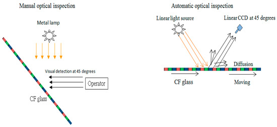
Figure 1.
Illustration of optical inspection, manual optical inspection (MOI) (left) vs automatic optical inspection (AOI) (right) [3,10].
The characteristics of non-uniformity due to chromaticity or thickness difference can be typically inspected by the related grey level variant. An edge detection method can be applied to compare the grey level between the background and the selected area. Then, the features of the binary image of the segmented region is compared with those in the database. Thus, the defects can be determined through proper thresholds.
In the progress of colour image extraction, several approaches and models have been developed for colour judgement and applied for colour differences. Among these, in relation to FPDs, the tristimulus method, established by the International Commission on Illumination (CIE), is very popular and has been applied to a diverse colour space through non-contact optical measurements, including colour gamut, colour shift, and chromaticity difference. The formulas for the CIE XYZ colour space are as follows:
In the above equations, CIE XYZ presents the tristimulus colour value which can be obtained through the spectrometer measurements. T() indicates the transmission spectrum and S() is a radiation profile for the illuminant C. Among the various colour systems, the CIE standard takes the spectrum response from the tristimulus values X, Y, and Z with the spectral matching functions x(λ), y(λ), and z(λ) to obtain the normalised chromaticity coordinates x, y, and z. By tristimulus values X, Y, Z, the chromaticity coordinates x, y, and z are obtained as follows [11]:
The colour difference ΔE is designed to distinguish the perceived colours quantitatively to judge colour deviation [12,13] and is generally used to classify various visibility levels to reflect the perceivable degree of colour difference by certain criteria [14]. ΔE is typically expressed in terms of the Euclidean distance and is an index of visual perceptibility between the background and foreground. Its threshold is determined through repeated measurements. It is treated as the perceptual analogy of colour appearance for human vision.
Furthermore, CIE presents the colour distance by the metric ΔE*ab, which occasionally is referred to as ΔE*, dE*, dE, or “Delta E”. The perceptual non-uniformities in the CIELAB colour space have led CIE to refine the definition over the years, leading to CIE1994 and CIEDE2000. These non-uniformities are important because human eyes are more sensitive to certain colour than others. A good metric should take this into account in order for the notion of “just noticeable difference” (JND) to be meaningful. Otherwise, a certain ΔE may be insignificant in one part of the colour space while being significant in some other part. However, currently, the criterion of the JND value for the colour difference to be just noticeable is not set universally, although in practice, the JND value of 1.0 is often used. Mahy et al. [15] studied and evaluated a JND value of 2.3 ΔE in 1994 . On the other hand, in the CIELAB colour space, the non-uniformity of perception is taken into account to reduce the inconsistency.
Berns [16] proposed the most prevalent methods to classify ΔEab, according to the perceptibility and acceptability. Initially, the perceptibility threshold determined the magnitude of colour difference of JND; a JND value of less than 1 implied the imperceptibility for viewing side by side [17]. Afterword, the acceptability was classified by three levels of colour difference for three visibilities of imperceptible, hardly perceptible, and easy perceptible sections. Furthermore, Perez et al. [18] determined the 50:50% perceptibility threshold (PT) and 50:50% acceptability threshold (AT) for computer-simulated samples of human gingiva using CIEDE2000 and CIELAB colour difference formulas. As a result, the PT and AT for CIEDE2000 and 95% confidence intervals were 1.1 and 2.8, respectively; the corresponding CIELAB values were 1.7 and 3.7. Nussbaum [17] proposed that two colour samples could be classified using ΔEab of less than 0.2 as “non-visible”, between 0.2 and 1.0 as “very small visual”, between 1.0 and 3.0 as “small”, between 3.0 and 6.0 as “medium”, and greater than 6.0 as “large”.
The JND is a quantitative index to describe the minimal amount of variation in a stimulus perceived by an observer; it has a statistical nature. In the display industry, the CIE xyY standard colour systems usually adopt the spectrum response from the tristimulus values X, Y, and Z that are used to obtain the normalised chromaticity coordinates x, y, and z. Through the transformation of the CIE xyY colour coordinates, the coordinates (a, b) in the CIELAB uniform colour space are as follows:
The symbols Xn, Yn, and Zn express the constant for the daylight source. The equations for colour difference are as follows:
In the above equations, ΔL, Δa, and Δb are the difference between the test and reference specimens in lightness, redness or greenness, and yellowness or blueness, respectively. The weighting factor K depends on the specific application; SL, SC, and SH are the compensation factors for lightness, chroma, and hue, respectively; whereas ΔL’, ΔC’, and ΔH’ are the specific lightness, chroma, and hue in ΔE2000. It has been found that the colour space of the colour difference formula of CIELAB is not completely uniform.
Figure 2 presents a schematic of the proposed architecture that detects the spot defects onto the LCD panel and measures the chromaticity of the panel. The conveyor reduces the tact time to increase the throughput of the production line. The system will send out an alarm message when a defect is detected.

Figure 2.
An installation for AOI engaged chromatic measurement by optical device.
3. Experimental Procedure
The present AOI method utilizes a VIS transmission chromatic spectrometer, Etaoptik (with a wavelength of 380 nm~1050 nm, focal length of 50 mm, detector: Si diode line array) to detect the non-uniformity defects on the green emission layer of the colour filter of the 6th generation (1500 mm × 1850 mm) TFT-LCD panels. The experiments were conducted in the class 1000 clean-room at 25 °C. The symmetric architecture uses a photo sensor linking image-grab card to acquire the two-dimensional image information. The line-scan TDI-CCD composes the multi array of the pixel sensors, DALSA HS-80-08K40 (dynamic range of 56 dB, line rates up to 34 kHz and throughput up to 320 MHz). The large panel substrate moved with constant speed for the whole sample scanning. The illuminant C source illuminated the area covered by the TDI-CCD.
Typically, four kinds of spot non-uniformity defects on the green layer were to be evaluated. They are labelled as A1, A2, B1, and B2 in Figure 3. Both A1 and A2 were the samples with artificial defects at 20 mm in diameter, which were dark regions and thick films of low transparency. In contrast, both B1 and B2 (also manmade defects of the same diameters of 20 mm) were bright regions and thin films with high transparency. After obtaining the image data, the embedded software identified the grey level variations to judge whether the threshold was reached to reveal the defect.
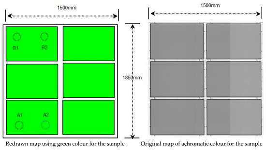
Figure 3.
Defect locations of the 6th generation in TFT-LCD panel.
4. Results and Discussion
Figure 4 shows the different spectral distributions for emissive layers of red, green, blue, and black matrices (BMs) through the spectrometer. The spectrum analysis is by 0.8 nm interval wavelength (BTC611E, back-thinned CCD array, working wavelengths from 300 nm to 1050 nm, produced by B&W TEK). Among these photo resists (PRs), the optical response of green layer reaches 65%, i.e., having larger power intensity than other PRs.

Figure 4.
Spectral profile for red, green, blue, and black matrices, respectively [3].
Figure 5 depicts the CIE x profiles across the spot defect at intervals of 1 mm for A1 and A2. This task identifies the chromatic tendency versus transparency. As shown, both A1 and A2 have a concave variation due to the dark region as well as the low transparency. Thus, CIE x on green emission layer exhibits the concave variation in the dark region.
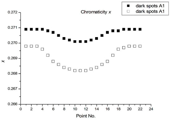
Figure 5.
Variation of CIE x for dark spots defect of A1 and A2.
Figure 6 shows the CIE x profiles across the spot defect at intervals of 1 mm for B1 and B2. As shown, both B1 and B2 have a convex variation as they are bright region and have high transparency. Thus, CIE x on green emission layer shows the convex variation in the bright region, and vice versa.
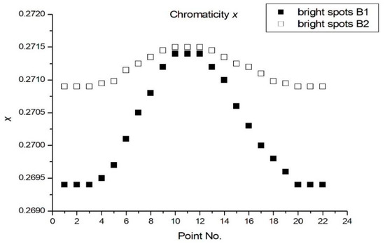
Figure 6.
Variation of CIE x for bright spots of B1 and B2.
Figure 7 illustrates that the CIE y variation for samples A1 and A2 (dark region and low transparency) have a convex characteristic. The CIE y demonstrates a proportional film thickness; a larger chromaticity with a thicker film and vice versa [14]. For the evaluation of colour variation, the chromaticity of CIE y is also used to judge the blue layer film in the flat panel industry [14,19].

Figure 7.
Variation of CIE y for dark spots of A1 and A2.
Figure 8 shows that the CIE y variation of samples B1 and B2 have a concave feature. The CIE y demonstrates a proportional film thickness; the larger chromaticity with the thicker film and vice versa. Hence, Figure 5, Figure 6, Figure 7 and Figure 8 indicate the variation of colour saturation with film transparency. For dark defects A1 and A2, delta_x > 0 and delta_y > 0, the saturation increases; for bright defect B, the reserve is observed. This behavior is expected for a color film thickness variation since decreasing the film thickness not only increasing its transmission but also widening its spectral width; hence decreasing the color saturation [14]. In the limiting case, when the film thickness drops to zero, its transmittance becomes 1 and the saturation falls to 0, corresponding to a colorless full transparent region.

Figure 8.
Variation of CIE y for bright spots of B1 and B2.
The CIE Y as shown in Figure 9 exhibits the luminance of the dark regions when the transmitted light passes through the region of spot non-uniformity. The transmitted light always decreases with thickness, regardless of the transparent material. The thin film has high transparency and the thick film has low transparency. It is obvious that the luminance of the transmitted light Y increases with transparency, being higher for thinner film regions (B defects as Figure 10) and lower for thicker regions (A defects as Figure 9). Thus both A1 and A2 have a concave variation with thick film, and both B1 and B2 are convex variation with thin film.
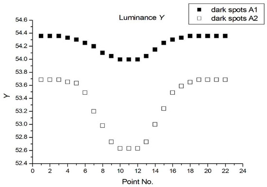
Figure 9.
Variation of CIE Y for dark spots defects of A1 and A2.

Figure 10.
Variation of CIE Y for bright spots defect of B1 and B2.
Figure 11 presents the dark spots A1 and A2 of the original map and the enhanced grey map with the associated CIE y variation. The original map was acquired by the line-scan TDI-CCD in grey levels from 0 to 255. The enhanced map was obtained from the original map by rescaling the grey levels from 0–255 to 120–170 by Photoshop to increase the image contrast of the dark spots. Thus, the defects have sharper image than original map. Moreover, the maximum CIE y differences are 0.001 and 0.004 for spot A1 and A2, respectively. The profile indicates that CIE y increases with thick film [14].

Figure 11.
The original map and enhanced map illustrate CIE y variation for A1 and A2.
Figure 12 illustrates the original map and enhanced grey with respect to CIE y variations for the bright spots B1 and B2. The maximum differences in CIE y are 0.002 and 0.001 for B1 and B2, respectively. The same grey rescaling scheme as did for A1 and A2 was also performed here to obtain sharper images of the defects. The profile indicates that CIE y decreases as the film thickness decreases, similar to the observations of [14].

Figure 12.
The original map and enhanced map illustrating defects by CIE y variations for B1 and B2, respectively.
Figure 13 presents the distribution of the colour gamut of the defects, A1, A2, B1, and B2 based on CIE xyY colour space. The triangle area uses the mathematical vector to depict the colour space. It shows that the imaging quality of colour saturation is very poor due the defects. Assuming the blue and red colours in the chromaticity are equivalent to the NTSC standard. Usually, the colour gamut can reveal the colour saturation, vivid, sharp, as well as contrast in the full colour of the display. The chart shows that these defects result in deficient colour saturation. As a result, the defects are more perceptual in the display.

Figure 13.
Colour gamut for A1, A2, B1, and B2.
Figure 14 presents the architecture of the calibrated spectrometer linking 198Hg discharged lamp which utilizes spectral lines to calibrate the spectrometer in the visual spectrum [20,21,22]. This calibrated apparatus adopts the Model 6034 pencil lamp from Oriel Instruments. The criterion for the shift of the wavelength is small than 1 pixel for the spectrometer; 1 pixel calculation based on the spectrometer capacity is the difference between the maximum value and the minimum value divided by the spectrometer resolution. In this task, 1 pixel is at (1050 − 380)/256 = 2.6 nm. The measurement standard deviation is at 0.8 nm for the spectrometer.
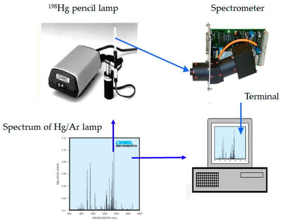
Figure 14.
Measurement procedure of 198Hg pencil lamp.
Table 1 lists the ranges of various CIE xyY for the examined defects. The results were obtained by repeating measurements ten times for each sample. The ranges of CIE x are 0.001, 0.002, 0.002, and 0.001 for samples A1, A2, B1, and B2, respectively. The corresponding ones for CIE y are 0.001, 0.004, 0.002, and 0.001; 0.4, 1.1, 0.7, and 0.4 for CIE Y. The maximum variation of CIE Y occurs in A2.

Table 1.
Statistics for colour variation for CIE xyY.
Table 2 tabulates the JND statistic according to colour difference referring to the formula of CIE1976, CIE1994, and CIEDE2000, indicating the visual intensity. Except for A2, these defect samples are imperceptible by human eyes. The ΔE colour differences of A2 are 3.3, 1.3, and 1.0 for CIE1976, CIE1994, and CIE2000, respectively, i.e., it is an obvious defect. The optical detected results show that the spot non-uniformity defects can be identified, even if the chromatic differences in CIE x and CIE y are below 0.001. In contrast, the colour gamut comparing to the 100% standard of NTSC shows that those of defects A1, A2, B1, and B2 are 75.31%, 76.43%, 75.10%, and 74.98%, respectively. That is, they result in very poor colour saturation; also, a high colour difference leads to a low colour gamut. With the sensitivity of the present AOI, it is more reliable than MOI as only A2 is perceptible, whereas the others are hardly perceptible by human assessors. For completeness, Table 3 tabulates the 198Hg discharge lamp with spectral lines to identify the standard deviation of spectral measurement to show the accuracy of the present AOI method.
Table 2.
Colour differences based on 1976, 1994, and 2000 formula, and colour gamut.
Table 3.
Standard deviation of the spectrometer by calibrated 198Hg discharged lamp.
5. Conclusions
An automatic optical method using a line-scan mode TDI-CCD with a transmitted spectrometer to detect non-uniformity of the green emission layer for ultra-high resolution TFT-LCDs is presented. The evidence shows a significant breakthrough to identify spot non-uniformity related to chromatic variation, and even JND is lower than the perceptibility threshold of a human assessor. Moreover, the CIE x of the green emission layer shows the concave variation for the dark region and the convex variation for the bright region. The CIE y is proportional film thickness, i.e., the larger chromaticity with the thicker film and vice versa. On the other hand, for CIE Y, both A1 and A2 have a concave variation with thick film, and both B1 and B2 have a convex variation with thin film. The present AOI has capacity of reaching the intensity of colour difference of 0.3 based on ΔE2000, which is more sensitive than that of the JND. Moreover, it can detect all of the defects samples investigated, but MOI can only detect defect A2; other defects are hardly perceptible by MOI. That is, the present method can quantify the defects accurately, and thus can substitute MOI in the display industry.
Author Contributions
Data curation, F.-M.T.; Formal analysis, F.-M.T.; Methodology, F.-M.T.; Validation, J.-H.C.; Writing–original draft, F.-M.T.; Writing–review & editing, F.-M.T. and J.-H.C.
Funding
This research received no external funding.
Conflicts of Interest
The authors declare no conflicts of interest.
References
- Liu, S.; Wang, D.; Yang, Z.K.; Feng, X.; Sun, X.; Qiu, Y. Key technology trends analysis of TFT-LCD. Chin. J. Liq. Cryst. Disp. 2018, 33, 457–463. [Google Scholar]
- Li, X.H.; Bao, J.P.; Xu, B.; Fan, H.Y. Improvement research of TFT-LCD module black uniformity. Chin. J. Liq. Cryst. Disp. 2018, 33, 271–276. [Google Scholar]
- Tzu, F.M.; Chou, J.H. Non-uniformity evaluation of flat panel display by automatic optical detection. In Proceedings of the 11th International Microsystems, Packaging, Assembly and Circuits Technology Conference (IMPACT), Taipei, Taiwan, 26–28 October 2016; pp. 168–171. [Google Scholar]
- Kwon, K.J.; Kim, M.B.; Heo, C.; Kim, S.G.; Baek, J.S.; Kim, Y.H. Wide color gamut and high dynamic range displays using RGBW LCDs. Displays 2015, 40, 9–16. [Google Scholar] [CrossRef]
- Kim, D.U.; Kim, J.S.; Choi, B.D. A Low-Power Data Driving Method With Enhanced Charge Sharing Technique for Large-Screen LCD TVs. J. Disp. Technol. 2015, 11, 346–352. [Google Scholar] [CrossRef]
- Bergman, L.; McHale, J.L. Handbook of Luminescent Semiconductor Materials; CRC Press: Boca Raton, FL, USA, 2016; pp. 268–270. [Google Scholar]
- Nam, G.; Lee, H.; Oh, S.; Kim, M.H. Measuring Color Defects in Flat Panel Displays Using HDR Imaging and Appearance Modeling. IEEE Trans. Instrum. Meas. 2016, 65, 297–304. [Google Scholar] [CrossRef]
- Kuo, C.F.; Hsu CT, M.; Fang, C.H.; Chao, S.M.; Lin, Y.D. Automatic defect inspection system of colour filters using Taguchi-based neural network. Int. J. Prod. Res. 2013, 51, 1464–1476. [Google Scholar] [CrossRef]
- Ali AS, O.; Asirvadam, V.S.; Malik, A.S.; Eltoukhy, M.M.; Aziz, A. Age-Invariant Face Recognition Using Triangle Geometric Features. Int. J. Pattern Recognit. Artif. Intell. 2015, 29, 1556006. [Google Scholar]
- Tzu, F.M.; Chou, J.H. Spot Mura evaluation in TFT-LCDs using automatic optical inspection. In Proceedings of the 5th International Microsystems Packaging Assembly and Circuits Technology Conference, Taipei, Taiwan, 20–22 October 2010; Volumes 1–4. [Google Scholar]
- Gomez-Polo, C.; Munoz, M.P.; Lunego MC, L.; Vicente, P.; Galindo, P.; Casado, A.M.M. Comparison of the CIELab and CIEDE2000 color difference formulas. J. Prosthet. Dent. 2016, 115, 65–70. [Google Scholar] [CrossRef] [PubMed]
- Strocka, D. Color difference formulas and visual acceptability. Appl. Opt. 1971, 10, 1308–1313. [Google Scholar] [CrossRef] [PubMed]
- Gomez-Polo, C.; Munoz, M.P.; Luengo MC, L.; Vicente, P.; Galindo, P.; Casado, A.M.M. Comparison of two color-difference formulas using the Bland-Altman approach based on natural tooth color space. J. Prosthet. Dent. 2016, 115, 482–488. [Google Scholar] [CrossRef] [PubMed]
- Tzu, F.M.; Chou, J.H. Slit-Mura Detection through Non-contact Optical Measurements of In-Line Spectrometer for TFT-LCDs. IEICE Trans. Electron. 2009, 92, 364–369. [Google Scholar] [CrossRef]
- Mahny, M.; Vaneycken, L.; Oosterlinck, A. Evaluation of uniform color spaces developed after adoption of CIELAB and CIELUV. Color Res. Appl. 1994, 19, 105–121. [Google Scholar]
- Berns, R.S. Billmeyer and Saltzman’s Principles of Color Technology; Wiley: New York, NY, USA, 2000. [Google Scholar]
- Nussbaum, P. Colour Measurement and Print Quality Assessment in a Colour Managed Printing Workflow. Doctoral Dissertation, The Norwegian Color Research Laboratory, Faculty of Computer Science and Media Technology, Gjøvik University College, Gjøvik, Norway, 2011; pp. 264–284. [Google Scholar]
- Perez, M.M.; Ghinea, R.; Herrera, L.J.; Carrillo, F.; Ionescu, A.M.; Paravina, R.D. Color difference thresholds for computer-simulated human Gingiva. J. Esthet. Restor. Dent. 2018, 30, E24–E30. [Google Scholar] [CrossRef] [PubMed]
- Lee, J.Y.; Yoo, S.I. Automatic detection of region-mura defect in TFT-LCD. IEICE Trans. Inf. Syst. 2004, 87, 2371–2378. [Google Scholar]
- Martinsen, P.; Jordan, B.; McGlone, A.; Gaastra, P.; Laurie, T. Accurate and precise wavelength calibration for wide bandwidth array spectrometers. Appl. Spectrosc. 2008, 62, 1008–1012. [Google Scholar] [CrossRef] [PubMed]
- Veza, D.; Salit, M.L.; Sansonetti, C.J.; Travis, J.C. Wave numbers and Ar pressure-induced shifts of Hg-198 atomic lines measured by Fourier transform spectroscopy. J. Phys. B At. Mol. Opt. Phys. 2005, 38, 3739–3753. [Google Scholar] [CrossRef]
- Sansonetti, C.J.; Salit, M.L.; Reader, J. Wavelengths of spectral lines in mercury pencil lamps. Appl. Opt. 1996, 35, 74–77. [Google Scholar] [CrossRef] [PubMed]
© 2018 by the authors. Licensee MDPI, Basel, Switzerland. This article is an open access article distributed under the terms and conditions of the Creative Commons Attribution (CC BY) license (http://creativecommons.org/licenses/by/4.0/).