R-curve Evaluation of Copper and Nickel Single Crystals Using Atomistic Simulations

1
College of Mechanics and Materials, Hohai University, Nanjing 211100, China
2
Department of Mechanical Engineering, Inha University, Incheon 402-751, Korea
*
Author to whom correspondence should be addressed.
Crystals 2018, 8(12), 441; https://doi.org/10.3390/cryst8120441
Submission received: 19 October 2018
/
Revised: 21 November 2018
/
Accepted: 22 November 2018
/
Published: 26 November 2018
Abstract
:The technique of molecular statics (MS) simulation was employed to determine the crack growth resistance curve of Cu and Ni single crystals. Copper and Ni single crystal nanoplates with an edge crack subjected to a tensile displacement were simulated. Stress-displacement curves and snapshots of the atomic configuration corresponding to different displacement levels were presented to elucidate the deformation mechanism. It was observed that the edge crack propagated step by step in a brittle manner, and the amount of crack growth at each step was half the lattice parameter. Through an energy consideration, the critical strain energy release rate at the onset of crack propagation and the crack growth resistance were calculated. The crack growth resistance is larger than the critical strain energy release rate because of the crack growth effect.
1. Introduction
Nanostructured materials have attracted considerable attention from both research communities and technology companies, due to their amazing optical, thermal, mechanical, electrical, and magnetic properties [1,2,3,4,5]. The past several decades have witnessed their wide application in nanoelectromechanical systems such as sensors, actuators, resonator, piezoelectric nanogenerators, and oscillators. Cracks may be introduced into these devices during the fabrication process. In addition, external mechanical or thermal loading may lead to the nucleation of cracks. A crack may arrest or propagate in a solid, depending on the loading condition as well as on the crack growth resistance (R), which characterizes the material’s resistance to crack growth. Therefore, a thorough knowledge of the R-curve of nanomaterials is crucial for the design of nanoelectromechanical devices.
Many experimental techniques have been developed to measure the R-curve of engineering materials, including single-edged-notched bending [6], single-edged-notched tension [7], three-point bending [8], compact tension [9], and double-edge-crack tension [10]. In experiments, R is calculated by formulae derived fromthe framework of continuum mechanics, which assumes that a solid is continuous. Continuum mechanics works quite well for bulk materials. However, when the size of materials reduces to nanoscale, the role of lattice discreteness on fracture properties is significant, and therefore the validity of continuum mechanics is debatable [11].
Atomistic simulation is a powerful technique to examine the mechanical behaviors of materials. Many interesting phenomena have been observed by atomistic simulations [12,13,14,15]. Particularly, lattice discreteness and the fundamental process of bond breaking can be captured by an atomistic simulation, which makes it an ideal tool for studying the fracture of nanomaterials. The use of atomistic simulations has furthered our understanding of fracture behaviors of materials. The critical strain for crack propagation in a Ni single crystal is affected by defects, and it may increase or decrease compared to the defect-free system, depending on the defect configuration [16]. Impurity point defects influence the critical load for crack initiation in Ni, Cu, and Au single crystals and the change resulting from point defects depends on defect species, geometry, and position [17]. The stress distribution in a single crystal Ni is affected by the microstructure evolution ahead of the crack tip [18]. Fracture behaviors and the critical strain energy release rate for crack propagation of Cu single crystals are dependent on crack length [19]. Nevertheless, no attempt has been made to measure the R-curve of materials by means of an atomistic simulation.
This study focused on the measurement of R-curve of nanomaterials based on atomistic simulations. Two face centered cubic (FCC) single crystals of Cu and Ni were chosen as the test samples. The fracture behaviors of Cu and Ni nanoplates with an edge crack subjected to a tensile load were examined by molecular statics (MS) simulations. The crack growth resistance and the critical strain energy release rate were evaluated based on an energy consideration. The crack growth resistance exceeds the critical strain energy release rate due to the crack growth effect.
2. Materials and Methods
Molecular statics simulations of the tensile deformation of Cu and Ni single crystal nanoplates with an edge crack were conducted at 0 K using the open source molecular dynamics (MD) program called the large-scale atomic/molecular massively parallel simulator (LAMMPS) [20]. The MS technique was used instead of MD method with an aim to avoid the extreme high strain rates associated with MD simulations [21,22]. Molecular statics simulations have been widely used to study crack growth behavior in solids [21,22]. The atomic configurations were visualized by AtomEye [23].
The atomic model of the nanoplate is illustrated in Figure 1. The x1, x2, and x3 axes of the simulation model were aligned along the [100], [010], and [001] directions, respectively. A periodic boundary condition was imposed in the x3 direction, whereas non-periodic boundary conditions were applied in the x1 and x2 directions. The model dimensions in the x1, x2, and x3 directions were w = 50a, 2h = 50a, and t = 5a, respectively, where a is the lattice parameter equal to 0.3615 nm and 0.352 nm for Cu and Ni, respectively. Four different crack lengths (c = 25a, 25.5a, 26a, and 27a) were employed to examine the effect of the crack length.
In order to guarantee the accuracy of the simulation results, a reliable interatomic potential is important. The interactions between atoms in the Cu and Ni systems were described by the embedded atom method (EAM) potentials developed by Mishin et al. [24] and Mishin et al. [25], respectively. These two potential functions, parameterized by an optimized systematic fitting to a vast database of both experimental and ab initio data, have been broadly employed in simulations of mechanical behavior of FCC metals, and the obtained results were in close agreement with the experimental results [26,27,28,29]. The virial stress expression [30], which is equivalent to the continuum level Cauchy stress [31], was used to calculate the stress components of the simulation system.
After creating the atomic model, an edge crack was introduced to the simulation system by cutting a given number of interatomic bonds between two consecutive (010) planes [17,32]. The system was then relaxed to the equilibrium state by applying the conjugate gradient method. Rebonding of the crack did not occur, since the interactions between atoms on the upper and lower crack surfaces were turned off. Subsequently, a stepwise tensile loading was applied to the model. The atoms in the boundary regions at the left upper and lower corners were displaced by a displacement of v in the x2 direction, as shown in Figure 1, followed by a relaxation process. The size of each boundary region is a × a × 5a. Many loading methods have been proposed to study fracture of materials by experiments, including single-edged-notched bending, single-edged-notched tension, three-point bending, compact tension, and double-edge-crack tension. The loading method applied in this work is similar to the compact tension method used in experiment. It should be noted that the crack growth resistance curve may be affected by loading method, which is left for future study. This displacement and relaxation procedure was repeated until the final failure of the nanoplate. A series of increments were used when applying the displacement to the system, and the simulation results converged when the increment was reduced to 5 × 10⁻⁵h. Thus, the displacement increment was selected to be 5 × 10⁻⁵h to alleviate the calculation burden without sacrificing the accuracy. The dislocation extraction algorithm (DXA) [33] and central symmetry parameter [34] were applied to detect dislocations and other defects in the simulation system.
3. Results and Discussion
3.1. Tensile Stress-Displacement Curves of the Cu Nanoplates
To elucidate the deformation mechanism of cracked Cu nanoplates subjected to a tensile displacement, the tensile stress (σ) of the simulation system is presented in Figure 2 as a function of v/h. Here, σ is calculated by averaging the atomic stress (σ22) over the entire volume of the simulation model, and v/h is the normalized tensile displacement. It should be noted that the tensile stress exhibits a similar trend to the tensile displacement variation regardless of the initial edge crack length. Specifically, the tensile stress-displacement curves can be divided into three stages: the linear stage, the nonlinear stage, and the declining stage. To demonstrate the deformation process, snapshots of the atomic configuration corresponding to these three stages were captured, as shown in Figure 3.
In the linear stage, the tensile stress increased linearly with increasing tensile displacement and the nanoplate deformed in a linear elastic manner. The distance between the surfaces on either side of the crack increased gradually with no dislocations or other defects nucleating in the nanoplate. In addition, the slope of the stress-displacement curves decreases with increasing crack length, which may indicate that an increased crack length results in a decreased stiffness of the nanoplate. This observation is in accordance with the result presented in a previous work [19].
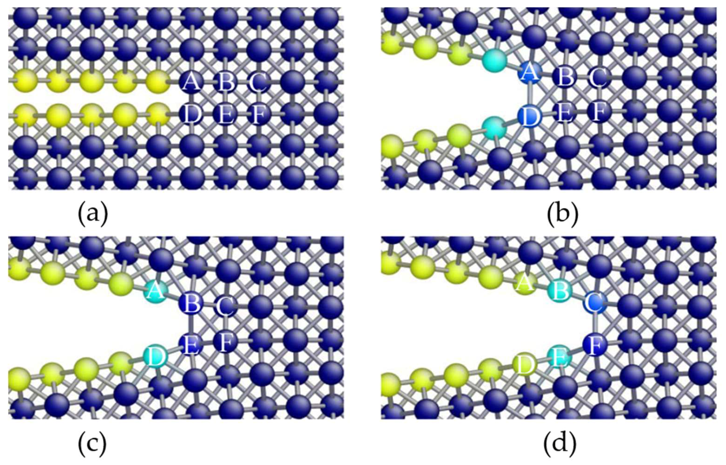
Following the linear stage, there is a short nonlinear stage before the peak stress point. In this stage, the tensile stress rises in a nonlinear manner and the increasing trend is more gradual. No dislocation or any other plastic deformation occurs in this stage. In order to uncover the deformation mechanism behind this nonlinear response, snapshots of the atomic configuration near the crack tip at different displacement levels were captured and shown in Figure 4. All atoms are colored according to the central symmetry parameter, and the bonds between the atoms are shown. For determining whether a bond is broken, an empirical cutoff distance of 0.3086 nm is used, which is halfway between the first and second neighbor shells of Cu [35]. A similar method has been used in previous works to describe the crack propagation process [36,37]. It should be noted that atoms shown in this figure are on two (001) planes. At the crack tip, the crack surfaces are bonded together by three bonds (bonds AD, AE, and BD), which are defined as the crack tip bonds. Upon the application of a tensile displacement, the length of the crack tip bonds increases gradually, and when the tensile displacement approaches the critical value, the AD bond ruptures first (Figure 4c). With a further increase in the tensile displacement, the BD bond snaps (Figure 4d), which is followed by the rupture of the AE bond (Figure 4e). After the snap of all three crack tip bonds, the edge crack is considered to have propagated by 0.5a. This asynchronous rupture of the three crack tip bonds might induce the nonlinear response of the tensile stress to the applied displacement.
After reaching the peak point, the tensile stress comes to its declining stage. In this stage, a sharp drop in the tensile stress is followed by a gradual increase, and this dropping/increasing trend repeats until the final failure of the nanoplate. The sharp drop is due to the abrupt propagation of the edge crack. The edge crack extends in a brittle manner and thus the crack surfaces are very flat and smooth, as shown in Figure 3, which is in close agreement with the previous observation that a Cu single crystal with a long edge crack exhibits a brittle fracture behavior [19]. Interestingly, after the first sharp descent, the stress-displacement curves of c = 25a and c = 25.5a coincide with the curves of c = 25.5a and c = 26a, respectively, and the stress-displacement curve of c = 26a coincides with that of c = 27a after two sharp drops. Hence, it is speculated that a sharp drop in the tensile stress is associated with an extension of the edge crack by 0.5a. This speculation is verified by the evolution of the crack tip structure, from which it can be observed that the edge crack extends by 0.5a at each drop point (Figure 4f). In contrast to the first extension of the edge crack, all three crack tip bonds snap simultaneously at each sharp drop point. It can be noted that the slope of the rising curve after each sharp drop decreases gradually and appears to decrease to zero when the displacement is very large, suggesting that the stiffness of the nanoplate decreases with the growth of the edge crack.
3.2. Tensile Stress-Displacement Curves of the Ni Nanoplates
For comparison, the tensile stress-displacement curves for the Ni nanoplates are presented in Figure 5. The tensile stress-displacement curves for the Ni nanoplates are similar to those of the Cu nanoplates except that there is no nonlinear stage in the Ni nanoplates, i.e., their tensile stress increases linearly to the peak value and then experiences the declining stage. To investigate the deformation mechanism, snapshots of the atomic configuration corresponding to various displacement levels are presented in Figure 6, from which it can be observed that the Ni nanoplate deforms elastically. The crack surfaces are clean and flat, indicating that the edge crack propagates in a brittle manner, consistent with previous results [16,18].
To elucidate the origin of the difference in the stress-displacement curve between the Cu and Ni nanoplates, several snapshots showing the atomic structure evolution near the crack tip of the Ni nanoplate are given in Figure 7. Bonds between atoms are shown, and an empirical cutoff distance of 0.3005 nm is used, which is halfway between the first and second neighbor shells of Ni [35,36,37]. Atoms shown in this figure are on two (001) planes. It can be observed that the crack tip bonds are gradually elongated in the linear stage by the tensile displacement, which is analogous to the case of the Cu nanoplate. However, after the linear stage, instead of an asynchronous rupture, all three crack tips snap synchronously. Therefore, there is no nonlinear stage for the Ni nanoplate since the asynchronous rupture of crack tip bonds does not occur. Similar to Cu, the edge crack propagates step by step and the amount of crack extension at each step is 0.5a, which is demonstrated by the crack tip structure evolution shown in Figure 7.
3.3. Evaluation of the R-curve
The energy required for the formation of crack surface with unit area is defined as the crack surface energy. Based on this definition, the crack surface energy for a single crystal can be expressed as
where γs is the crack surface energy, E0 is the potential energy per unit thickness without any external loading, and ΔE0(c) = E0(c + Δc) − E0(c). From the MS simulations, the crack surface energies for the Cu and Ni nanoplates were evaluated. After the creation of a simulation system with an edge crack of length c, a relaxation process was performed to attain the potential energy per unit thickness E0(c). Subsequently, the length of the edge crack was enlarged by Δc and the simulation system was relaxed to obtain E0(c + Δc). Here, Δc was chosen to be 0.5a. The crack surface energy was then calculated using Equation (1) with the results for the Cu and Ni nanoplates shown in Figure 8. The obtained surface energies are in close agreement with previous results [24,25].
The strain energy release rate is a measure of the available energy for an increment of crack extension [38]. According to this definition, the strain energy release rate for a single crystal can be written as:
where G is the strain energy release rate, U is the strain energy per unit thickness resulting from the external loading, E is total potential energy per unit thickness for a loaded system, and ΔU(c) = U(c + Δc) − U(c) for a given v. Using Equations (1) and (3), Equation (2) can be rewritten as
where ΔE(c) = E(c + Δc) − E(c) for a given v.
According to the conventional fracture mechanics, crack propagation occurs once G reaches a critical value:
where Gc is the critical strain energy release rate, which is a measure of fracture toughness. Since the surface energy has been evaluated and E can be obtained from the MS simulations, the strain energy release rate can easily be calculated from Equation (4). Consistent with the calculation of the crack surface energy, Δc was taken as 0.5a. The numerical results of Gc for the Cu and Ni nanoplates are plotted in Figure 8. It deserves to be mentioned that the first sharp drop point was taken as the onset point of crack propagation, although the edge crack in the Cu nanoplate propagates by 0.5a through an asynchronous rupture of crack tip bonds before the first sharp drop in the tensile stress.
The crack growth resistance, R, is defined as the rate at which energy is dissipated in the process of crack growth [39]. In consideration of the energy rate balance, the values of G and R are equivalent at each instant of crack propagation. Therefore, Equation (4) can be used to evaluate the R. In the aforementioned discussion, the edge crack propagates step by step in the Cu and Ni nanoplates, and the increment of the crack length at each step is 0.5a. Thus, based on the E obtained from the MS simulations, R was calculated using Equation (4). The results of the calculated R for the Cu and Ni nanoplates are presented in Figure 8 as a function of the amount of crack growth. In accordance with the calculation of Gc, the first sharp drop point was considered as the starting point of crack growth.
The crack growth resistance of the Cu nanoplate increased slightly with crack growth, converging rapidly to 2γs, which is the fracture toughness predicted by the Griffith theory [40], as shown in Figure 8a. It should be noted that the Gc is lower in comparison to R. To explain the reason behind this deviation between the Gc and R, one must recall their physical meanings. The Gc is the fracture toughness for a stationary crack, while R is the fracture toughness for a growing crack. Therefore, it is conjectured that the discrepancy between the Gc and R can be attributed to the effect of crack growth. In addition, the Gc is slightly smaller than 2γs, which is in good agreement with previous studies on fracture properties of single crystal Cu and NaCl [17,41,42].
The crack growth resistance curve of the Ni nanoplate exhibits a slightly different trend compared to the Cu nanoplate. Instead of a monotonic increase, the R of the Ni nanoplate rises relatively rapidly during the process of crack growth by a, and with a further growth of the crack by 0.5a, the R decreases slightly. Following this slight decline, the R increases gradually and appears to converge to a stable value after the crack extends by 6a. In contrast to Cu, the R-curve of Ni nanoplates converges to a value which is approximately 10% larger than 2γs. Moreover, the Gc is also observed to be greater than 2γs. The R and Gc differ from 2γs because of the lattice trapping [43] arising from the discreteness of the lattice. This observation is consistent with the results of previous work on the fracture behavior of single crystal Ni [16,17]. Similar to the case of Cu, the R of Ni nanoplates is higher than the Gc because of the effect of the crack growth.
4. Conclusions
The crack growth resistance curves of Cu and Ni single crystals were investigated by means of MS simulations. The fracture behaviors of the Cu and Ni nanoplates with an edge crack under a tensile displacement were simulated. The edge crack propagated step by step in a brittle manner in both the Cu and Ni nanoplates, with an extension of half the lattice parameter at each step. Through an energy analysis, the crack growth resistance and critical strain energy release rate were calculated. The crack growth resistance is higher than the critical strain energy release rate because of the crack growth effect.
Author Contributions
X.R.Z. and H.G.B. conceived and designed the study; X.R.Z. and J.H.K. performed the simulations; X.R.Z., J.H.K., and H.G.B. analyzed the results and wrote the paper.
Funding
This research was supported by the Basic Science Research Program through the National Research Foundation of Korea (NRF), funded by the Ministry of Education, Republic of Korea (Grant No. NRF-2013R 1A 1A2A 10008799). Zhuo was supported by the Fundamental Research Funds for the Central Universities (Grant No. 2017B01214) and the China Postdoctoral Science Foundation (Grant No. 2018M632214).
Acknowledgments
In this section you can acknowledge any support given which is not covered by the author contribution or funding sections. This may include administrative and technical support, or donations in kind (e.g., materials used for experiments).
Conflicts of Interest
The authors declare no conflict of interest.
References
- Yang, P.; Yan, H.; Mao, S.; Russo, R.; Johnson, J.; Saykally, R.; Morris, N.; Pham, J.; He, R.; Choi, H.J. Controlled Growth of ZnO Nanowires and Their Optical Properties. Adv. Funct. Mater. 2010, 12, 323–331. [Google Scholar] [CrossRef]
- Balandin, A.A.; Ghosh, S.; Bao, W.; Calizo, I.; Teweldebrhan, D.; Miao, F.; Lau, C.N. Superior thermal conductivity of single-layer graphene. Nano Lett. 2008, 8, 902. [Google Scholar] [CrossRef] [PubMed]
- Kang, K.; Cai, W. Size and temperature effects on the fracture mechanisms of silicon nanowires: Molecular dynamics simulations. Int. J. Plast. 2010, 26, 1387–1401. [Google Scholar] [CrossRef]
- Cui, Y.; Duan, X.; Hu, J.; Lieber, C.M. Doping and electrical transport in silicon nanowires. J. Phys. Chem. B 2000, 104, 5213–5216. [Google Scholar] [CrossRef]
- Whitney, T.M.; Searson, P.C.; Jiang, J.S.; Chien, C.L. Fabrication and magnetic properties of arrays of metallic nanowires. Science 1993, 261, 1316–1319. [Google Scholar] [CrossRef] [PubMed]
- Zhou, D.W. Measurement and modelling of R-curves for low-constraint specimens. Eng. Fract. Mech. 2011, 78, 605–622. [Google Scholar] [CrossRef]
- Hou, F.; Hong, S. Characterization of R-curve behavior of translaminar crack growth in cross-ply composite laminates using digital image correlation. Eng. Fract. Mech. 2014, 117, 51–70. [Google Scholar] [CrossRef]
- Bornhauser, A.; Kromp, K.; Pabst, R.F. R-curve evaluation with ceramic materials at elevated temperatures by an energy approach using direct observation and compliance calculation of the crack length. J. Mater. Sci. 1985, 20, 2586–2596. [Google Scholar] [CrossRef]
- Rödel, J.; Seo, Y.H.; Benčan, A.; Malič, B.; Kosec, M.; Webber, K.G. R-curves in transformation toughened lead zirconatetitanate. Eng. Fract. Mech. 2013, 100, 86–91. [Google Scholar] [CrossRef]
- Pinho, S.T.; Robinson, P.; Iannucci, L. Fracture toughness of the tensile and compressive fibre failure modes in laminated composites. Compos. Sci. Technol. 2006, 66, 2069–2079. [Google Scholar] [CrossRef] [Green Version]
- Ippolito, M.; Mattoni, A.; Colombo, L.; Pugno, N. Role of lattice discreteness on brittle fracture: Atomistic simulations versus analytical models. Phys. Rev. B 2006, 73, 4111. [Google Scholar] [CrossRef]
- Cheng, Y.; Zhu, P.; Li, R. The influence of vertical vibration on nanoscale friction: A molecular dynamics simulation study. Crystals 2018, 8, 129. [Google Scholar] [CrossRef]
- Yi, D.; Li, J.; Zhu, P. Study of nanoscratching process of GaAs using molecular dynamics. Crystals 2018, 8, 321. [Google Scholar] [CrossRef]
- Zhuo, X.R.; Beom, H.G. Size-dependent torsional deformation of silicon nanowires. Mater. Lett. 2018, 213, 48–50. [Google Scholar] [CrossRef]
- Zhuo, X.R.; Beom, H.G. Atomistic study of the bending properties of silicon nanowires. Comput. Mater. Sci. 2018, 152, 331–336. [Google Scholar] [CrossRef]
- Karimi, M.; Roarty, T.; Kaplan, T. Molecular dynamics simulations of crack propagation in Ni with defects. Model. Simul. Mater. Sci. Eng. 2006, 14, 1409. [Google Scholar] [CrossRef]
- Petucci, J.; Leblond, C.; Karimi, M. Molecular dynamics simulations of brittle fracture in fcc crystalline materials in the presence of defects. Comput. Mater. Sci. 2014, 86, 130–139. [Google Scholar] [CrossRef]
- Wu, W.P.; Yao, Z.Z. Molecular dynamics simulation of stress distribution and microstructure evolution ahead of a growing crack in single crystal nickel. Theor. Appl. Fract. Mech. 2012, 62, 67–75. [Google Scholar] [CrossRef]
- Cui, C.B.; Beom, H.G. Molecular dynamics simulations of edge cracks in copper and aluminum single crystals. Mater. Sci. Eng. A 2014, 609, 102–109. [Google Scholar] [CrossRef]
- Plimpton, S. Fast parallel algorithms for short-range molecular dynamics. J. Comput. Phys. 1995, 117, 1–19. [Google Scholar] [CrossRef]
- Farkas, D. Fracture Resistance of Nanocrystalline Ni. Metall. Mater. Trans. A 2007, 38, 2168–2173. [Google Scholar] [CrossRef]
- Andric, P.; Curtin, W.A. New theory for Mode I crack-tip dislocation emission. J. Mech. Phys. Solids 2017, 106, 315–337. [Google Scholar] [CrossRef]
- Li, J. AtomEye: An efficient atomistic configuration viewer. Model. Simul. Mater. Sci. Eng. 2003, 11, 173. [Google Scholar] [CrossRef]
- Mishin, Y.; Mehl, M.J.; Papaconstantopoulos, D.A.; Voter, A.F.; Kress, J.D. Structural stability and lattice defects in copper: Ab initio, tight-binding, and embedded-atom calculations. Phys. Rev. B 2001, 63, 224106. [Google Scholar] [CrossRef]
- Mishin, Y.; Farkas, D.; Papaconstantopoulos, M.J.M.A. Interatomic potentials for monoatomic metals from experimental data and ab initio calculations. Phys. Rev. B 1999, 59, 3393–3407. [Google Scholar] [CrossRef] [Green Version]
- Swygenhoven, H.V.; Derlet, P.M. Grain-boundary sliding in nanocrystalline fcc metals. Phys. Rev. B 2001, 64, 224105. [Google Scholar] [CrossRef]
- Cahn, J.W.; Mishin, Y.; Suzuki, A. Coupling grain boundary motion to shear deformation. Acta Mater. 2006, 54, 4953–4975. [Google Scholar] [CrossRef]
- Zhuo, X.R.; Beom, H.G. Molecular statics simulations of the size-dependent mechanical properties of copper nanofilms under shear loading. Comput. Mater. Sci. 2015, 99, 390–395. [Google Scholar] [CrossRef]
- Jin, Z.H.; Gumbsch, P.; Albe, K.; Ma, E.; Lu, K.; Gleiter, H.; Hahn, H. Interactions between non-screw lattice dislocations and coherent twin boundaries in face-centered cubic metals. Acta Mater. 2008, 56, 1126–1135. [Google Scholar] [CrossRef]
- Zhuo, X.R.; Beom, H.G. Size-dependent fracture properties of cracked silicon nanofilms. Mater. Sci. Eng. A 2015, 636, 470–475. [Google Scholar] [CrossRef]
- Swenson, R.J. Comments on virial theorems for bounded systems. Am. J. Phys. 1983, 51, 940–942. [Google Scholar] [CrossRef]
- Subramaniyan, A.K.; Sun, C.T. Continuum interpretation of virial stress in molecular simulations. Int. J. Solids Struct. 2008, 45, 4340–4346. [Google Scholar] [CrossRef]
- Stukowski, A.; Bulatov, V.V.; Arsenlis, A. Automated identification and indexing of dislocations in crystal interfaces. Model. Simul. Mater. Sci. Eng. 2012, 20, 085007. [Google Scholar] [CrossRef] [Green Version]
- Kelchner, C.L.; Plimpton, S.J.; Hamilton, J.C. Dislocation nucleation and defect structure during surface indentation. Phys. Rev. B 1998, 58, 11085–11088. [Google Scholar] [CrossRef]
- Stukowski, A.; Albe, K. Extracting dislocations and non-dislocation crystal defects from atomistic simulation data. Model. Simul. Mater. Sci. Eng. 2010, 18, 085001. [Google Scholar] [CrossRef]
- Cheung, K.S.; Yip, S. Brittle-ductile transition in intrinsic fracture behavior of crystals. Phys. Rev. Lett. 1990, 65, 2804. [Google Scholar] [CrossRef] [PubMed]
- Huang, S.; Zhang, S.; Belytschko, T.; Terdalkar, S.S.; Zhu, T. Mechanics of nanocrack: Fracture, dislocation emission, and Amorphization. J. Mech. Phys. Solids 2009, 57, 840–850. [Google Scholar] [CrossRef]
- Anderson, T.L. Fracture Mechanics: Fundamentals and Applications; CRC Press: Boca Raton, FL, USA, 1991; pp. 635–636. [Google Scholar]
- Eftis, J.; Liebowitz, H. On fracture toughness evaluation for semi-brittle fracture. Eng. Fract. Mech. 1975, 7, 101–135. [Google Scholar] [CrossRef]
- Griffith, A.A. The Phenomena of Rupture and Flow in Solids. Philos. Trans. R. Soc. Lond. 1921, 221, 163–198. [Google Scholar] [CrossRef] [Green Version]
- Adnan, A.; Sun, C.T. Evolution of nanoscale defects to planar cracks in a brittle solid. J. Mech. Phys. Solids 2010, 58, 983–1000. [Google Scholar] [CrossRef]
- Sakib, A.R.N.; Adnan, A. On the size-dependent critical stress intensity factor of confined brittle nanofilms. Eng. Fract. Mech. 2012, 86, 13–22. [Google Scholar] [CrossRef]
- Thomson, R.; Hsieh, C.; Rana, V. Lattice Trapping of Fracture Cracks. J. Appl. Phys. 1971, 42, 3154–3160. [Google Scholar] [CrossRef]
Figure 1.
Atomic model geometry for the Cu and Ni nanoplates containing an edge crack of length c. A tensile displacement v is applied to the boundary regions located at the left upper and lower corners.
Figure 1.
Atomic model geometry for the Cu and Ni nanoplates containing an edge crack of length c. A tensile displacement v is applied to the boundary regions located at the left upper and lower corners.
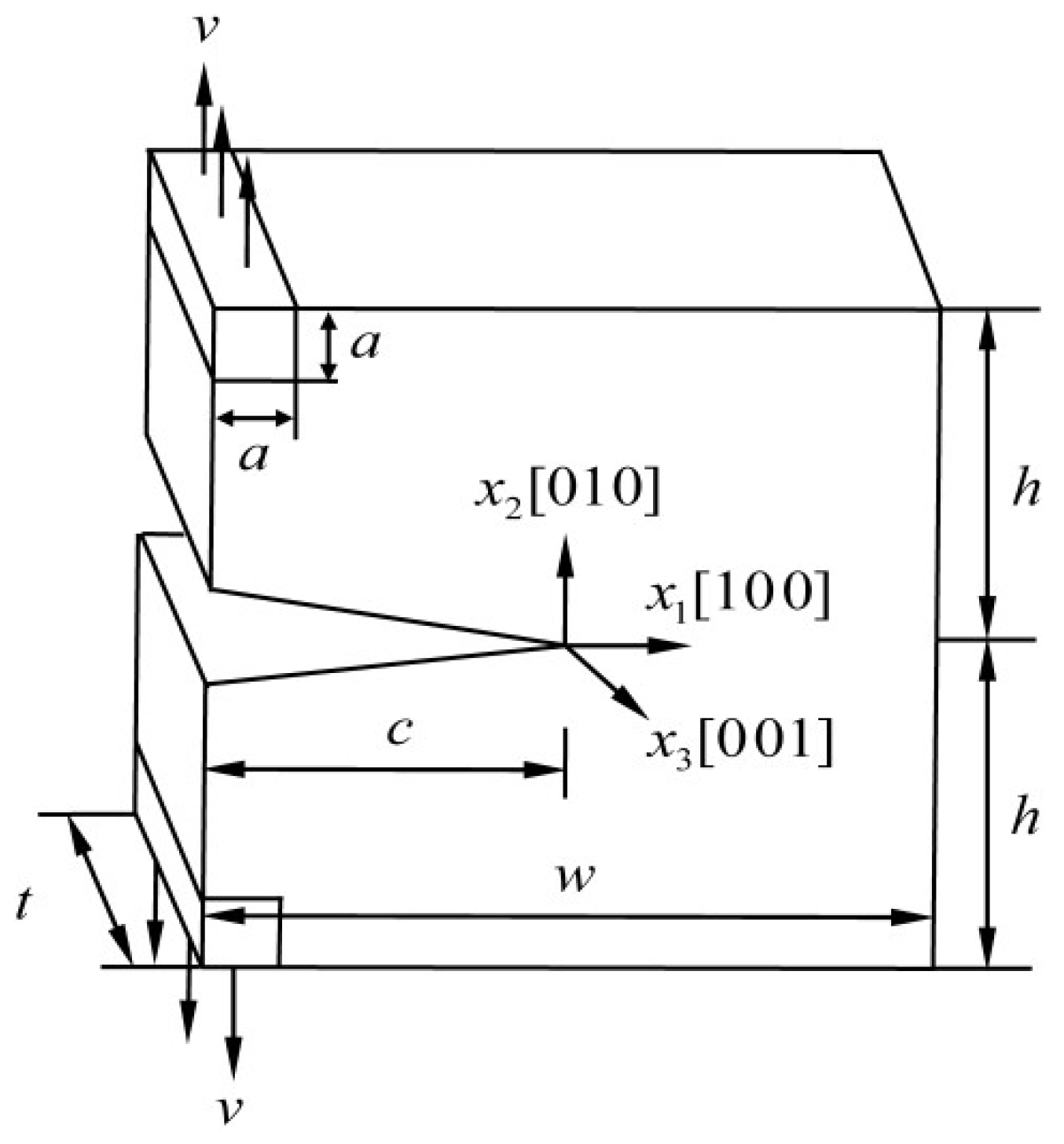
Figure 2.
Tensile stress (σ) of Cu nanoplates as a function of v/h for four lengths of edge crack: c = 25a, 25.5a, 26a, and 27a. σ is defined as the average value of the atomic stress (σ22) over the entire volume of the simulation system.
Figure 2.
Tensile stress (σ) of Cu nanoplates as a function of v/h for four lengths of edge crack: c = 25a, 25.5a, 26a, and 27a. σ is defined as the average value of the atomic stress (σ22) over the entire volume of the simulation system.
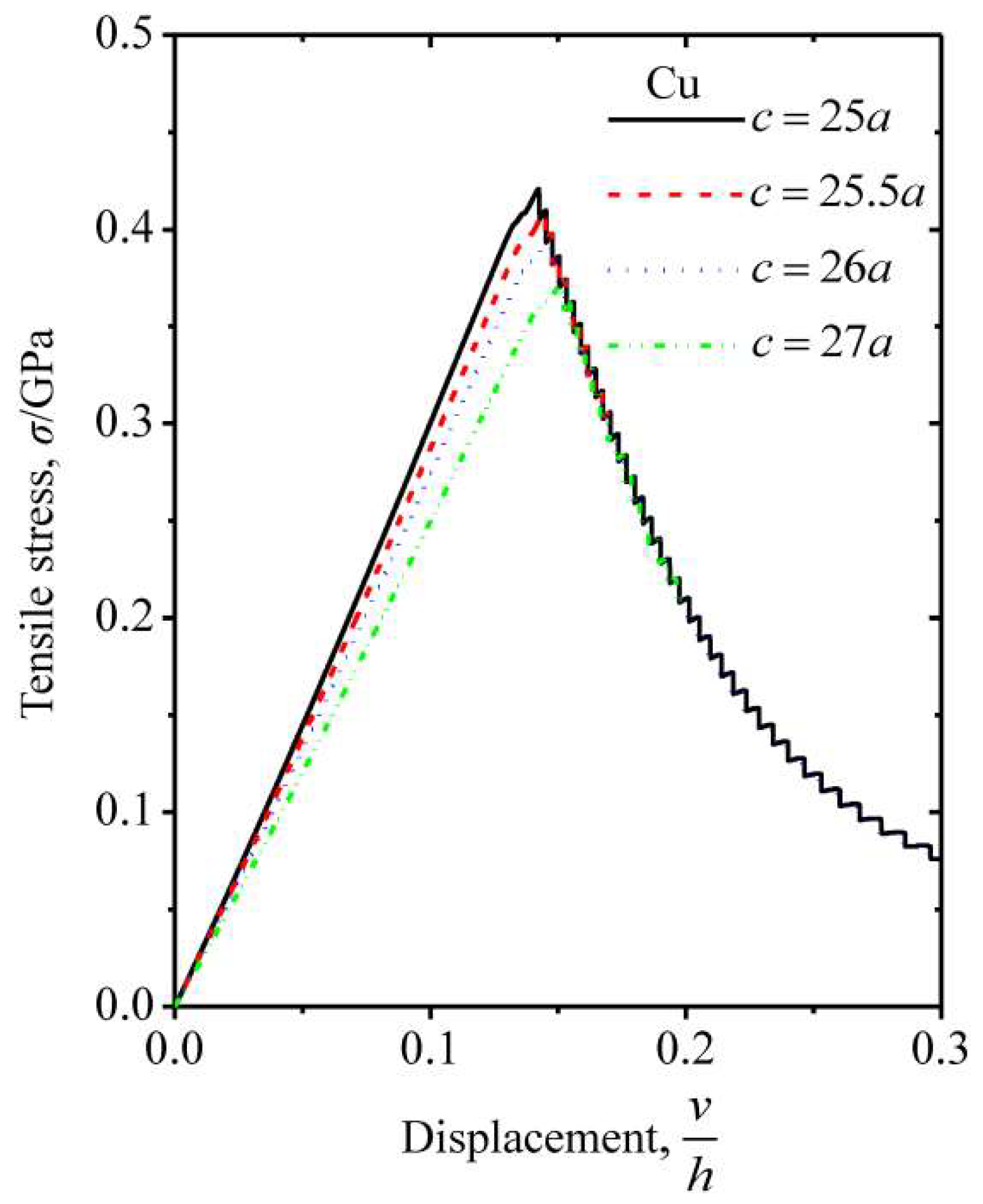
Figure 3.
Snapshots of the atomistic configuration corresponding to different stages of the Cu nanoplate with a crack length of 25c. Atoms are colored according to the σ22 component of the atomic stress, with blue indicatinglow stress and red representing high stress. (a) Initial relaxed state before applying tensile displacement. (b) The linear stage. (c) The nonlinear stage. (d) The declining stage.

Figure 4.
Snapshots of the Cu nanoplate crack tip structure with a crack length of 25c corresponding to various v/h levels. Atoms are colored according to the central symmetry parameter, and the bonds between atoms are shown. For determining whether a bond is broken, an empirical cutoff distance of 0.3086 nm is used, which is halfway between the first and second neighbor shells of Cu. It should be noted that atoms shown in this figure are on two (001) planes. (a) v/h = 0, (b) v/h = 0.13205, (c) v/h = 0.1321, (d) v/h = 0.13515, (e) v/h = 0.1352, and (f) v/h = 0.14785.

Figure 5.
Tensile stress (σ) of Cu nanoplates as a function of v/h for four lengths of edge crack: c = 25a, 25.5a, 26a, and 27a. σ is defined as the average value of the atomic stress (σ22) over the entire volume of the simulation system.
Figure 5.
Tensile stress (σ) of Cu nanoplates as a function of v/h for four lengths of edge crack: c = 25a, 25.5a, 26a, and 27a. σ is defined as the average value of the atomic stress (σ22) over the entire volume of the simulation system.
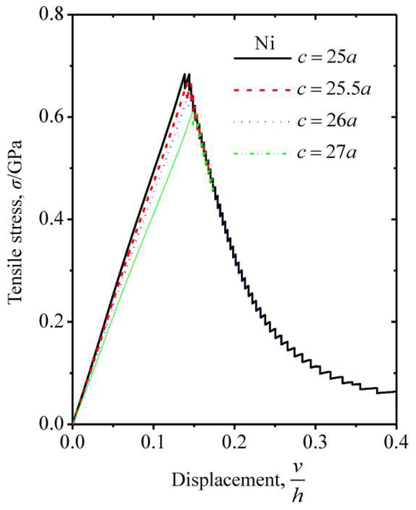
Figure 6.
Snapshots of the atomistic configuration corresponding to different stages of the Ni nanoplate with a crack length of 25c. Atoms are colored according to the σ22 component of the atomic stress, with blue indicatinglow stress and red representing high stress. (a) Initial relaxed state before applying tensile displacement. (b) The linear stage. (c) Immediately before the crack propagation. (d) The declining stage.
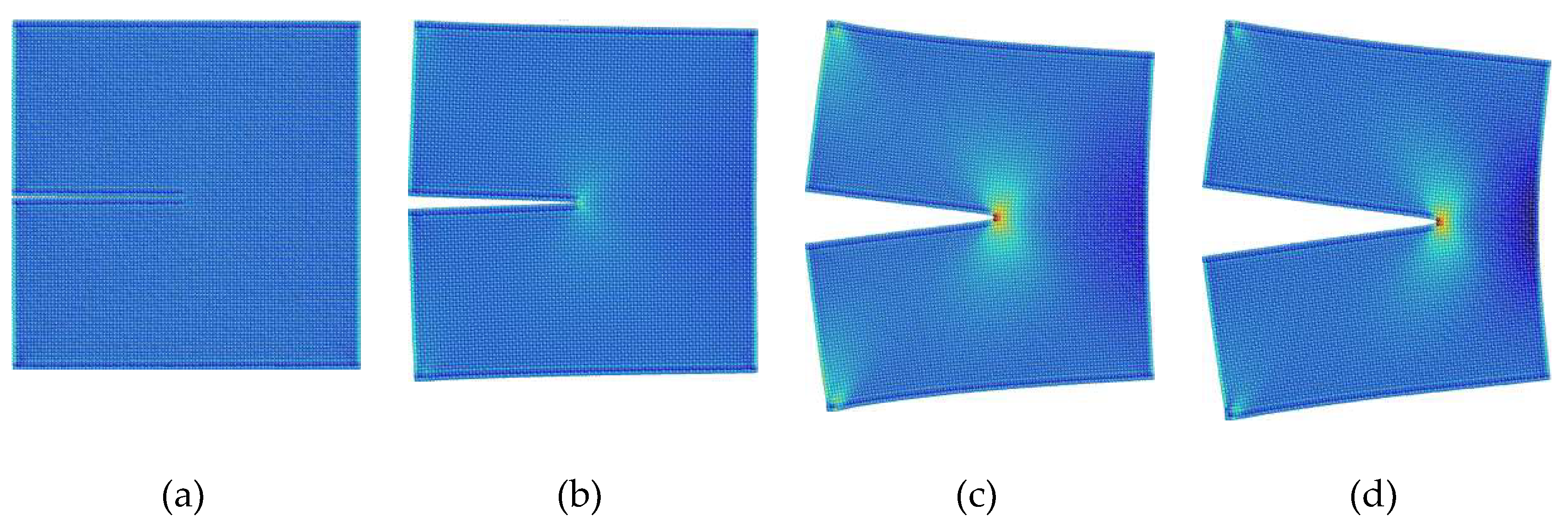
Figure 7.
Snapshots of the Ni nanoplate crack tip structure with a crack length of 25c corresponding to various v/h levels. Atoms are colored according to the central symmetry parameter, and the bonds between atoms are shown. For determining whether a bond is broken, an empirical cutoff distance of 0.3005 nm is used, which is halfway between the first and second neighbor shells of Ni. It should be noted that atoms shown in this figure are on two (001) planes. (a) v/h = 0, (b) v/h = 0.13855, (c) v/h = 0.1386, (d) v/h = 0.14405.

Figure 8.
(a) R-curve of the Cu nanoplate with a crack length of 25c. (b) R-curve of the Cu nanoplate with a crack length of 25c. Δc is the amount of crack growth. For comparison, the critical strain energy release rate at the onset of crack propagation (Gc) and the fracture toughness predicted by the Griffith criterion (2γs) are inserted.

© 2018 by the authors. Licensee MDPI, Basel, Switzerland. This article is an open access article distributed under the terms and conditions of the Creative Commons Attribution (CC BY) license (http://creativecommons.org/licenses/by/4.0/).
Share and Cite
MDPI and ACS Style
Zhuo, X.R.; Kim, J.H.; Beom, H.G. R-curve Evaluation of Copper and Nickel Single Crystals Using Atomistic Simulations. Crystals 2018, 8, 441. https://doi.org/10.3390/cryst8120441
AMA Style
Zhuo XR, Kim JH, Beom HG. R-curve Evaluation of Copper and Nickel Single Crystals Using Atomistic Simulations. Crystals. 2018; 8(12):441. https://doi.org/10.3390/cryst8120441
Chicago/Turabian StyleZhuo, Xiao Ru, Jang Hyun Kim, and Hyeon Gyu Beom. 2018. "R-curve Evaluation of Copper and Nickel Single Crystals Using Atomistic Simulations" Crystals 8, no. 12: 441. https://doi.org/10.3390/cryst8120441
Note that from the first issue of 2016, this journal uses article numbers instead of page numbers. See further details here.