Article

Thickness Study of Er-Doped Magnesium Zinc Oxide Diode by Spray Pyrolysis

1
Department of Electrophysics, National Chiao Tung University, Hsinchu 30010, Taiwan
2
Department of Electrical Engineering, National University of Kaohsiung, Kaohsiung 81148, Taiwan
3
National Chung-Shan Institute of Science & Technology, Taoyuan 32599, Taiwan
4
Department of Electronic Engineering, Minghsin University of Science and Technology, Hsinchu 30401, Taiwan
5
Department of Applied Physics, National University of Kaohsiung, Kaohsiung 81148, Taiwan
*
Author to whom correspondence should be addressed.
Crystals 2018, 8(12), 454; https://doi.org/10.3390/cryst8120454
Submission received: 12 October 2018 / Revised: 27 November 2018 / Accepted: 4 December 2018 / Published: 6 December 2018

Abstract

:
Erbium-doped magnesium zinc oxides were prepared through spray pyrolysis deposition at 450 °C with an aqueous solution containing magnesium nitrate, zinc acetate, erbium acetate, and indium nitrate precursors. Diodes with different erbium-doped magnesium zinc oxide thicknesses were fabricated. The effect of erbium-doped magnesium zinc oxide was investigated. The crystalline structure and surface morphology were analyzed using X-ray diffraction and scanning electron microscopy. The films exhibited a zinc oxide structure, with (002), (101), and (102) planes and tiny rods in a mixed hexagonal flakes surface morphology. With the photoluminescence analyses, defect states were identified. The diodes were fabricated via a metallization process in which the top contact was Au and the bottom contact was In. The current–voltage characteristics of these diodes were characterized. The structure resistance increased with the increase in erbium-doped magnesium zinc oxide thickness. With a reverse bias in excess of 8 V, the light spectrum, with two distinct green light emissions at wavelengths of 532 nm and 553 nm, was observed. The light intensity that resulted when using a different operation current of the diodes was investigated. The diode with an erbium-doped magnesium zinc oxide thickness of 230 nm shows high light intensity with an operational current of 80 mA. The emission spectrum with different injection currents for the diodes was characterized and the mechanism is discussed.

1. Introduction

Rare-earth-doped materials have been widely investigated in many applications in past decades [1,2,3,4,5]. Erbium (Er), one of the rare earth materials, has shown good performance in optoelectronic devices [6,7,8]. On the other hand, the wide bandgap II‒VI semiconductor zinc oxide (ZnO), which has a large exciton binding energy, is one of the most promising host materials in optoelectronic devices [8]. In a combination of the two materials, an Er-doped ZnO diode has shown Er-related green light luminescence performance [9]. However, a high reverse-biased operation is needed for the diode operation, which limits the device’s applications. Still, the luminescence spectrum of such a diode is in the green gap spectral range for developing InGaN diodes [10]. Moreover, the emission wavelength is also in the low transmission loss window of PMMA-core optical fiber [11]. This is promising for the development of similar diodes as the emission source in Si-based photonic applications [12].
In the operation of the Er-doped ZnO diode, an operational voltage in excess of the reverse bias breakdown condition is needed to achieve the carrier impact ionization condition to transfer the energy to Er-related emissions [9]. When considering the quality of host material, the low defect requirement is an important issue in the breakdown behavior [13,14]. In the ZnO host material, certain defects such as zinc interstitial (Zni) and oxygen vacancy (VO) are generally incorporated into the film. To improve this, it was found that some defect emissions in photoluminescence (PL) in ZnO can be reduced with the introduction of Mg [15]. The MgZnO device with suitable Mg content shows low dark current performance [16].
In ZnO-based material fabrication, many technologies can be applied [17,18,19]. The spray pyrolysis method is one of the best non-vacuum methods for ZnO deposition [20,21]. We investigated the diode performance of the ZnO:Er on a p-Si substrate by spray pyrolysis method in the previous study [22]. In this study, a diode with different MgZnO:Er active layer thickness was prepared on a Si substrate by the spray pyrolysis method. The film morphology, crystalline quality, and diode properties were investigated. The effect of the injection current on diode electroluminescence intensity and spectral properties was studied.

2. Experimental

A MgZnO:Er layer followed by a ZnO:In layer were deposited on a p-type silicon substrate ((111), 5 × 1018 cm−3) by the spray pyrolysis method at 450 °C. Two aqueous solutions were prepared in the fabrication of MgZnO:Er and ZnO:In layers. In the fabrication of the MgZnO:Er film, an aqueous solution mixed with 0.2 mol/L zinc acetate dihydrate (Zn(CH3COOH)2·2H2O, ZnAc), magnesium acetate tetrahydrate (Mg(CH3COOH)2·4H2O, MgAc) (Mg/Zn = 25 at %), and erbium acetate hydrate (Er(CH3COO)3·4H2O, ErAc) (Er/Zn = 5 at %) was prepared. In the fabrication of the ZnO:In film, an aqueous solution with 0.2 mol/L ZnAc, mixed with indium nitrate hydrate (In(NO3)3·5H2O, InNt) (In/Zn = 5 at %), was prepared. Before deposition, the aqueous solution was stirred for 1 h at room temperature to yield a clear solution. The 2 × 1 cm Si substrate, cut from the Si wafer, was cleaned with acetone, rinsed in DI water, dried by N2 gas, dipped in diluted HF (1:20), rinsed in DI water and dried by N2 gas. After that, the Si substrate was transferred to a deposition chamber. After a high-temperature stabilization step, the substrate temperature was fixed at 450 °C and the MgZnO:Er and ZnO:In layers were deposited sequentially. After the film deposition, In was deposited on the Si side by a thermal process. The front Au circular pad (0.8 mm diameter) was formed by a direct-current magnetron sputtering process with a shadow mask. The thickness of the MgZnO:Er/ZnO:In layer was 170 nm/100 nm, 230 nm/100 nm, and 550 nm/100 nm for samples ST1, ST2, and ST3, respectively. The films’ thickness was controlled with different deposition times after the thickness calibration runs. When considering the run-to-run deposition rate stability and thickness uniformity on the wafer, the thickness variation in the following device study was ±11%.
The surface morphology and cross-section of the samples were examined by scanning electron microscopy (SEM, Hitachi S-4300N, Tokyo, Japan). The element contents of the film were accomplished by XPS analysis (ESCALAB XI+, Thermo Fisher Scientific, Madison, WI, USA). The photoluminescence (PL) spectrum was obtained by an optical system with a spectrometer (HR2000+, Ocean Optics, Largo, FL, USA), He-Cd laser (325 nm wavelength), and a cryostat. The diode current–voltage and electroluminescence characters were examined by the spectrometer and source meter (Keithley 2400, Solon, OH, USA).

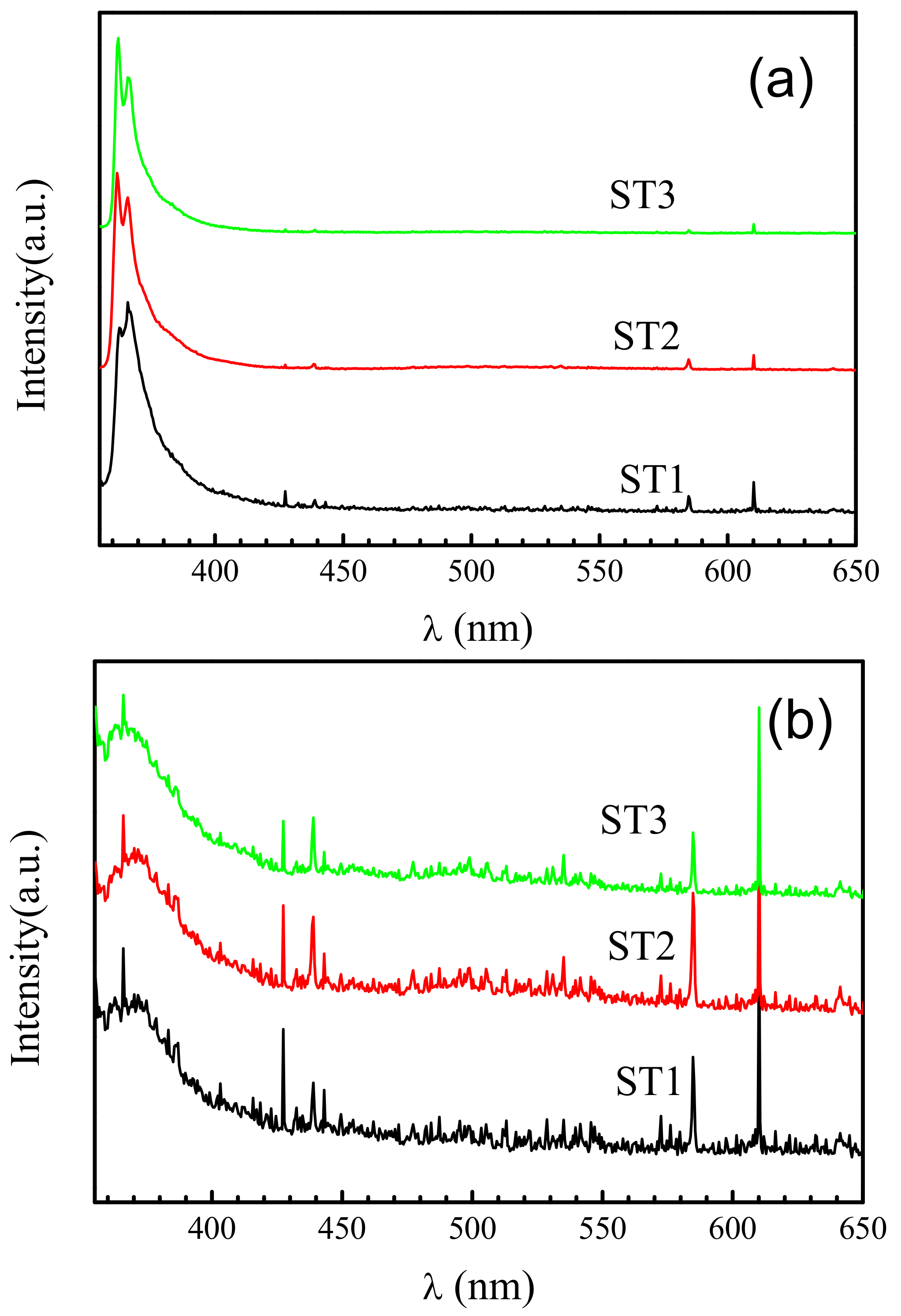
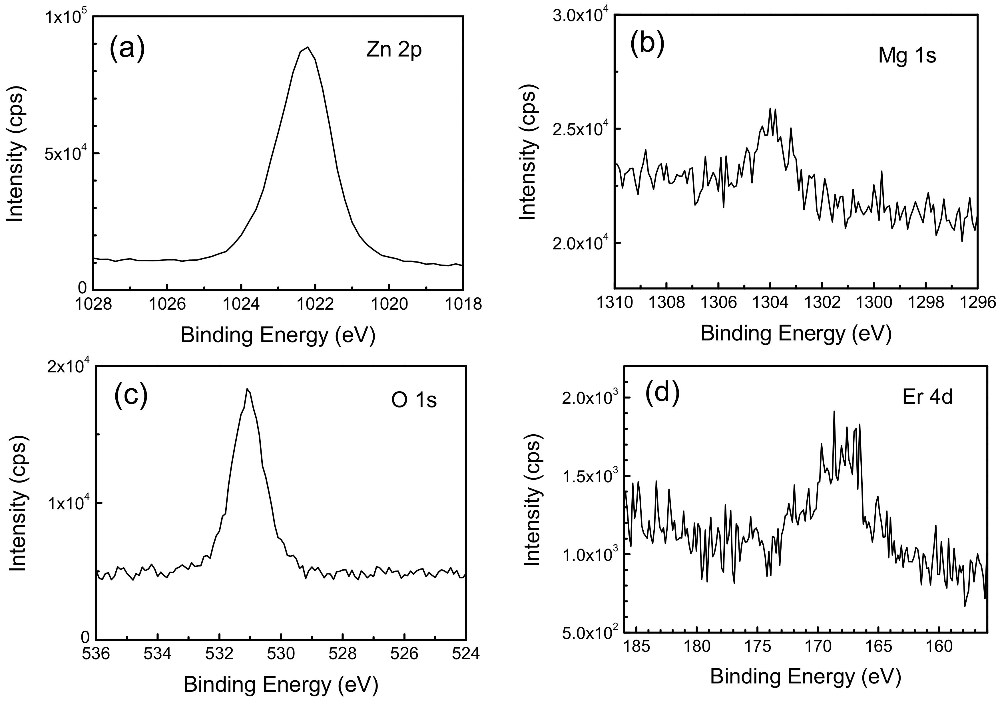
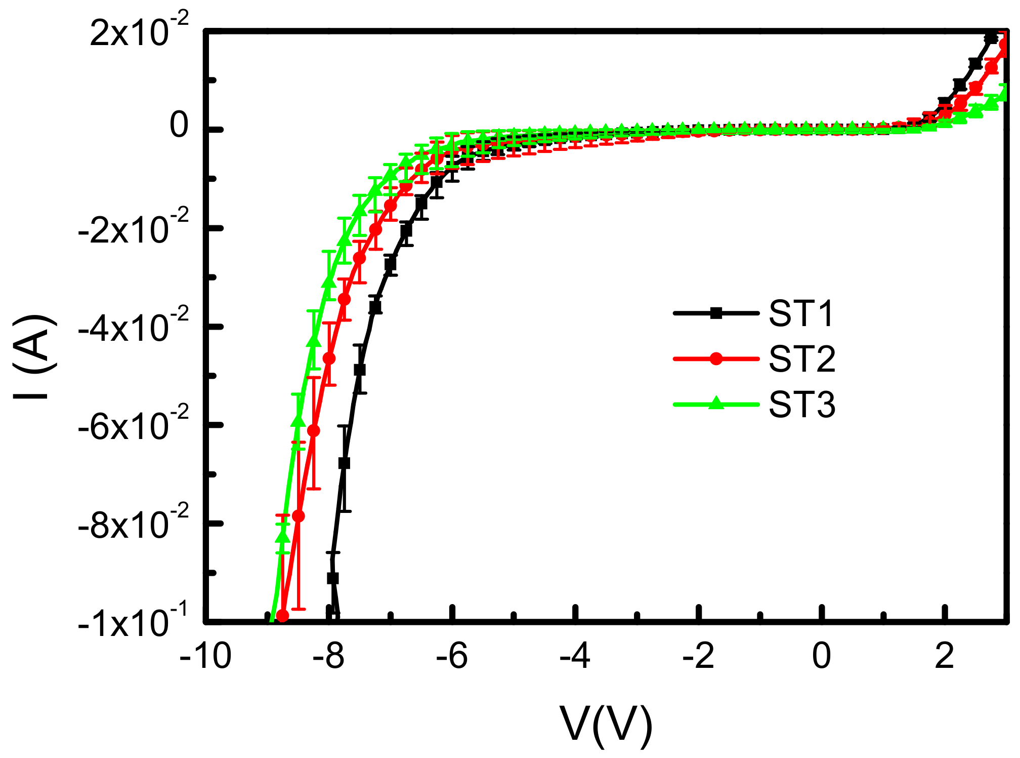
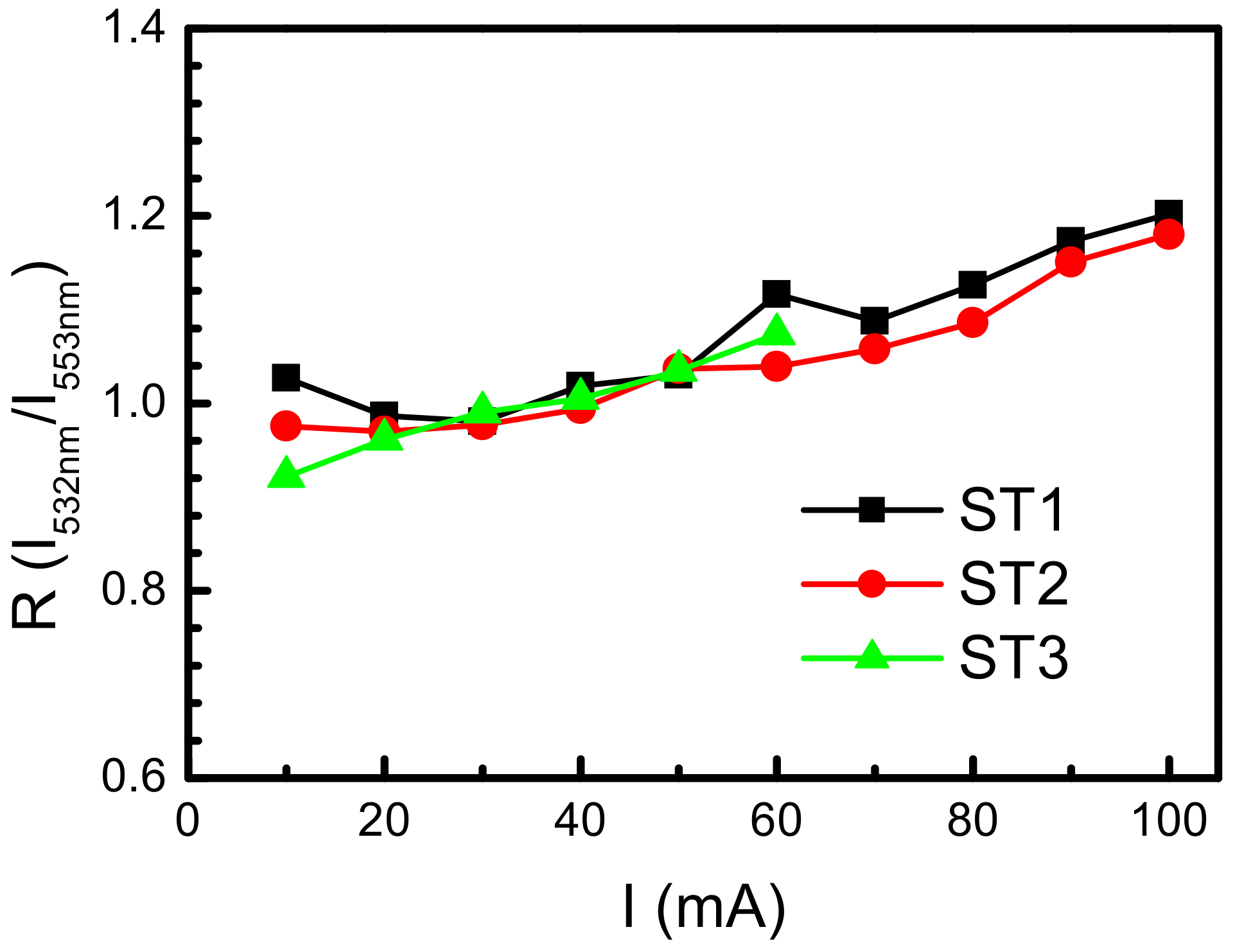
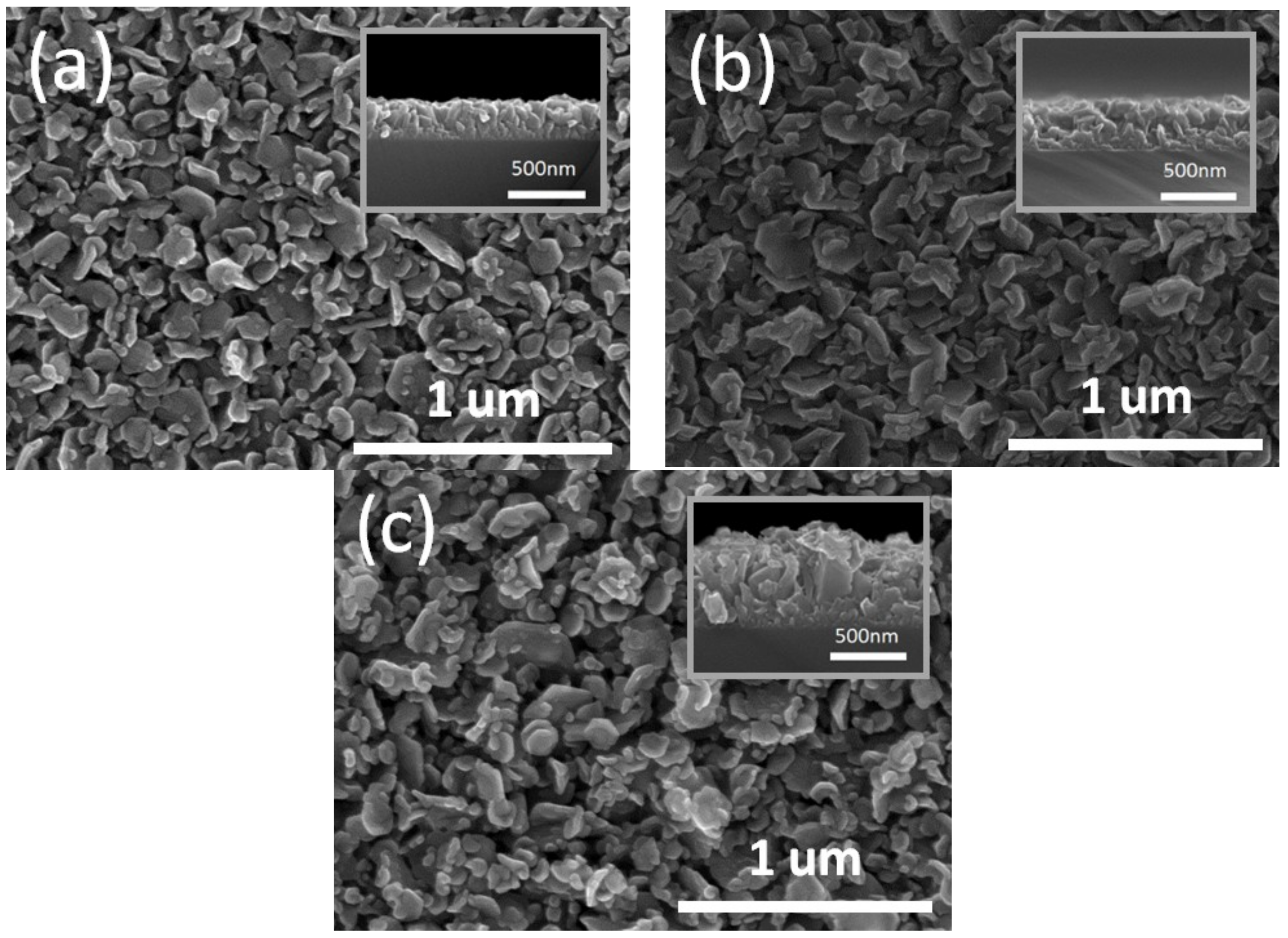
3. Results and Discussion

Figure 1 exhibits the surface morphology of samples ST1, ST2, and ST3. The cross-section of each sample is shown in the inset. The morphology, with different sized hexagonal flakes and tiny rods, can be observed. For ST1, a small-grained structure can be observed in the cross-section. With an increase in the MgZnO:Er deposition time, a similar surface morphology can be observed. However, some large grains in the cross-section in ST3 can be observed, while small grains formed near the Si/MgZnO:Er interface. The varied morphology may originate from the deposition nature [20,21] and deposition parameters [23] in the spray pyrolysis process.
The XRD patterns of samples ST1, ST2, and ST3 are shown in Figure 2. Three crystalline orientations, (002), (101), and (102), of the ZnO wurtzite structure were observed. For MgxZn1−xO, the MgO characteristic peak can be observed as phase separation occurred (x ≥ 0.4) [24]. For Er-doped ZnO, there is generally no Er2O3 characteristic peak that can be observed while the doping content is low [25]. As the Mg composition and Er content in the MgZnO:Er is low, there are no obvious MgO- [26] and Er2O3 [27]-related signals that can be observed. Regarding the peaks in Figure 2, the broad character is caused by the grain size effect [28] and the superposition of the two host materials, MgZnO and ZnO [29].
Figure 3a shows the PL spectrum of these samples measured at 10 K. Two peaks with wavelengths of 362.7 nm (3.42 eV) and 366.5 nm (3.38 eV) can be observed for all samples. The two emission peaks come from the MgZnO:Er layer, mainly as both emissions display a higher energy than the band gap emission of ZnO. Furthermore, as the energy difference for the two peaks is 40 meV, the near-band-edge (NBE) emission at 362.7 nm is attributed to the recombination of excitons bound to the neutral donor (DoX) and the emission at 366.5 nm is attributed to the two electron satellite (denoted as TES) transitions of the DoX [30,31]. With the optical band gap evaluated from NBE emission, the x quantity in the MgxZn1−xO:Er layer was estimated to be approximately 0.1 [32].
In the spectrum, a broad profile at a wavelength of 400 nm for all samples can be observed. The emission signal around 400 nm is attributed to the isolated VZn-related or OZn type [33]. Certain such defects exist in the diode. Moreover, no obvious emissions around a wavelength of 480‒520 nm [33,34] can be observed in the 10 K PL for all samples.
Figure 3b shows the PL spectrum of the samples measured at room temperature. Compared to the spectrum measured at 10 K, a NBE band with temperature broadening [30] and band gap narrowing [35,36] with a central wavelength at 368 nm was observed. A weak and broad blue emission (BE) around a wavelength of 500 nm can also be observed. The BE band was attributed to the carrier recombination between the extended zinc interstitial state and holes [37]. In PL measurement, the carriers were generated by a photo-exciting process and transported spatially. The emission was observed after the carrier recombination. The carrier spatial transport ability depends on the environmental temperature [38,39]. The inconsistency of the BE band for samples measured at 10 K and room temperature suggests the non-uniformed BE-related defect distribution in the samples. Furthermore, when we compare the PL spectra to those of the reported ZnO:Er diodes [9], the low BE band to NBE band intensity ratio (IBE/INBE) in our MgZnO:Er diode can be observed. A smaller BE-related defect may exist in our sample. This suggests the benefit of using MgZnO as the Er-doped layer.
For the Er-doped ZnO, no Er-related emission in the PL measurement can be observed generally. The Er-related PL band for the ZnO-based materials can be observed for the sample prepared after a high-temperature procedure [40,41,42]. The oxygen vacancy states may make a contribution to the PL emissions [42].
When discussing why there were no Er-related PL emissions in the ZnO host, Iwan et al. [9] suggest that the intra-atomic level transition of the Er ion saturates at a much lower excitation photon power compared to the band to band transition of the host material. Harako et al. [43] point out that the observed visible band electroluminescence (EL) of the ZnO:Er diode was attributed to the carrier causing impact excitations of Er ions rather than to the energy transformation from e‒h pairs in the ZnO host. Thus, the energy transform yield from e‒h pairs, as generated by the PL process, to Er ion states in the visible band may be quite low, which might account for the missing Er-related emissions in the visible band.
Figure 4 exhibits the XPS spectra of Zn 2p, Mg 1s, O 1s, and Er 4d in the MgZnO:Er layer of sample ST3. In Figure 4a, the Zn 2p3/2 signal with a peak energy of 1022 eV can be observed. The value is within the reported range for high-temperature annealed ZnO [44]. A distorted profile toward the high-energy side of Figure 4a can be observed. This is ascribed to Zn2+ in hydroxide [45], and originates in the spray pyrolysis process. In Figure 4b, the binding energy, 1304 eV, of the Mg 1s core level is observed [46]. In Figure 4c, the O1s signal with a peak energy of 531 eV was observed. This value is near the reported O2− on a normal wurtzite ZnO crystal (530.8 eV) [44,47]. The distorted shape in the high-energy side shows O2− in hydroxide [48]. Figure 4d shows the Er 4d5/2 signal. This broad profile may include the signal related to Er‒OH bonds (peak energy at 170.4 eV) and the signal related to Er‒O bonds (peak energy at 168.4 eV) [46]. The Er/Zn ratio in the film is estimated be 0.2% from the XPS characterization. As the atomic ratio of Er/Zn is 5% in the precursor, the incorporation efficiency of Er from ErAc is low compared to that of Zn from ZnAc in the spray pyrolysis deposition process.
Figure 5 shows the current‒voltage (I–V) characteristics of diodes ST1, ST2, and ST3, measured at room temperature. The error bars show the variations of the five diodes in each sample. A rectification character in forward bias and breakdown behavior in reverse bias can be observed. In the reverse bias region, the breakdown voltage increases with the increase in the MgZnO:Er layer’s thickness. As with the higher bandgap host material MgZnO, the samples show a small reverse bias current around −4 V compared to the reported ZnO:Er diodes [22]. On the other hand, the diode and series resistance (Rs) and ideality factor (n) that describe the diode can be extracted [48] and are listed in Table 1.
In Table 1, the quantities and variations of diode ideality n for considering five diodes on each sample were listed. Since n is 1 for the recombination of injected carriers in the neutral region, it is 2 for the carrier recombination by mediated recombination centers in the space charge region [49,50]. A high ideality factor with n greater than 2 can be observed in many diodes made from wide bandgap materials [51]. For the heterostructured diode with grained morphology in this work, the high ideality may arise from the effect of the heterojunction [52] and/or the high defect density [9] around the grain boundary in the MgZnO:Er layer. In Table 1, the high series resistance quantity for ST3 can be observed. For a film with a large grain, the boundary induced conduction is inhibited. Thus the high Rs from ST3 may come from the large grain as shown in Figure 1 and/or from the thick MgZnO:Er layer.
Figure 6 shows the electroluminescence spectra of ST1, ST2, and ST3 with different reverse biased injected current measured at room temperature. Figure 7 expresses the light intensity‒injection current (L‒I) characteristics of samples ST1, ST2, and ST3 measured at room temperature. The error bar for each measurement is shown. For the diode under high reverse bias, the electrons and holes, which were created and accelerated in the depletion region due to the high electric field, transfer the energy to excite Er ions by impact ionization [9,53,54] and cause the emissions of the diode. In Figure 4, two emission bands in the visible range related to the energy state transitions of Er3+ of 2H11/24I15/2 (around 532 nm) and 4S3/24I15/2 (around 553 nm) [55] can be observed. Compared to the reported emission spectra in the ZnO:Er diode [22], little spectral difference can be observed in the MgZnO:Er samples. The fine spectrum variation in the emission band is caused by the variation of the host structure [56].
In terms of the L‒I character of ST1, the light intensity shows an increasing‒remaining behavior with the increase in the injection current. The low light intensity of ST1 may originate from the thin MgZnO:Er active layer. For sample ST2, the light intensity increases with the increase in the injection current. The light intensity then begins to decrease when the injection current is in excess of 80 mA. The decreasing character originates from the joule heat generated under a high injection current [57,58]. For ST3 under operation, as the diode preserved a thick MgZnO:Er layer and a high overall series resistance, the joule heat accumulated heavily in the active region and thus caused damage to the diode with an injection current in excess of 60 mA.
Figure 8 shows the electroluminescence intensity ratio between the 2H11/24I15/2 transition (I532 nm) and the 4S3/24I15/2 (I553 nm) transition of the samples with different operational currents. The intensity ratio R(I532 nm/I553 nm) increases with the increase in the injection current. For the diode operating in an avalanche breakdown condition, the increased current was caused by the enhanced impact ionization due to the high reverse bias. The carriers preserved high impact energy in the case of a high injection current. The increase in the short wavelength emission intensity in 2H11/2 is due to the increase of high energy carrier impaction. This causes an increase in the intensity ratio R(I532 nm/I553 nm) with the increase in the injection current.

4. Conclusions

Heterostructured p-Si/MgZnO:Er/ZnO:In diodes with different MgZnO:Er active layer thicknesses were prepared by spray pyrolysis. The morphologies, crystalline properties, and diode characteristics were investigated. The surface morphology varied with the increase in film thickness. The diode series resistance increases with the increase in the MgZnO:Er layer. Two Er ions’ related green emissions were characterized. The emission intensity increased with the increase in the MgZnO:Er layer at a low injection current. With a thick MgZnO:Er layer operating at a high injection current, the diode represented worse emissions due to the high resistance. With the increase in the injection current, green emissions with a short wavelength had the advantage. The possible mechanisms were discussed.

Author Contributions

Individual contributions to this research. Conceptualization: Y.-T.H., W.-H.L. and K.-F.H., Methodology: Y.-T.H., C.-C.L., S.-Y.L., Validation: K.-J.C., J.-C.L., S.-Y.L., W.-J.L., Formal Analysis: W.-H.L., Investigation: W.-H.L., Data Curation: W.-H.L. and Y.-T.H., Writing—Original Draft Preparation: W.-H.L., M.-C.W. and C.-J.H., Writing—Review & Editing: W.-H.L., Visualization: W.-H.L.

Funding

This research was funded by the Ministry of Science and Technology, Taiwan (MOST 106-2221-E-390-012-, MOST 107-2221-E-390-013-), and National Chung Shan Institute of Science and Technology, R.O.C., NCSIST-104-V404(107).

Conflicts of Interest

The authors declare no conflict of interest.

References

  1. Gapontsev, V.P.; Matitsin, S.M.; Isineev, A.A.; Kravchenko, V.B. Erbium glass lasers and their applications. Opt. Laser Technol. 1982, 14, 189–196. [Google Scholar] [CrossRef]
  2. Kamik, S.A.; Chandrappan, J.; Murray, M.; Steenson, P.; Krauss, T.F.; Jose, G. Ultrafast laser plasma doping of Er3+ ions in silica-on-silicon for optical waveguiding applications. Opt. Lett. 2016, 41, 4684–4687. [Google Scholar]
  3. Irrera, A.; Miritello, M.; Pacifici, D.; Franzo, G.; Priolo, F.; Iacona, F.; Sanfilippo, D.; di Stefano, G.; Fallica, P.G. Electroluminescence properties of SiOx layers implanted with rare earth ions. Nucl. Instrum. Methods Phys. Res. B 2004, 216, 222–227. [Google Scholar] [CrossRef]
  4. Nakamura, K.; Takemoto, S.; Terai, Y.; Suzuki, M.; Koizumi, A.; Takeda, Y.; Tonouchi, M.; Fujiwara, Y. Direct observation of trapping of photo-excited carriers in Er, O-codoped GaAs. Phys. B 2006, 376–377, 556–559. [Google Scholar] [CrossRef]
  5. Fujiwara, Y.; Koizumi, A.; Urakami, A.; Yoshikane, T.; Inoue, K.; Takeda, Y. Room temperature 1.5 μm electroluminescnence from GaInP/Er,O-codoped GaAs/GaInP double heterostructure injection-type light emitting diodes grown by organometallic vapor phase epitaxy. Mater. Sci. Eng. B 2003, 105, 57–60. [Google Scholar] [CrossRef]
  6. Dahal, R.; Lin, J.Y.; Jiang, H.X.; Zavada, J.M. Room temperature 1.5 μm electroluminescnence from GaInP/Er,O-codoped GaAs/GaInP double heterostructure injection-type light emitting diodes grown by organometallic vapor phase epitaxy. Opt. Mater. 2011, 33, 1066–1070. [Google Scholar] [CrossRef]
  7. Nyk, M.; Kuzmin, A.; Prasad, P.N.; Strek, W.; de Araújo, C. Red up-conversion emission from nanocrystalline GaN powders co-doped with Er3+ and Yb3+. Opt. Mater. 2009, 31, 800–804. [Google Scholar] [CrossRef]
  8. Li, S.; Ye, S.; Liu, T.; Wang, H.; Wang, D. Enhanced up-conversion emissions in ZnO-LiYbO2: RE3+ (RE= Er or Ho) hybrid phosphors through surface modification. J. Alloy. Compd. 2016, 658, 85–90. [Google Scholar] [CrossRef]
  9. Iwan, S.; Bambang, S.; Zhao, J.L.; Tan, S.T.; Fan, H.M.; Sun, L.; Zhang, S.; Ryu, H.H.; Sun, X.W. Green electroluminescence from an n-ZnO: Er/p-Si heterostructured light-emitting diode. Phys. B 2012, 407, 2721–2724. [Google Scholar] [CrossRef]
  10. Saito, S.; Hashimoto, R.; Hwang, J.; Nunoue, S. InGaN Light-Emitting Diodes on c-Face Sapphire Substrates in Green Gap Spectral Range. Appl. Phys. Express 2003, 6, 111004. [Google Scholar] [CrossRef]
  11. Zubia, J.; Arrue, J. Plastic Optical Fibers: An Introduction to Their Technological Processes and Applications. Opt. Fiber Technol. 2001, 7, 101–140. [Google Scholar] [CrossRef]
  12. Jambois, O.; Berencen, Y.; Hijazi, K.; Wojdak, M.; Kenyon, A.J.; Gourbilleau, F.; Rizk, R.; Garrido, B. Current transport and electroluminesc ence mechanisms in thin SiO2 films containing Si nanocluster-sensitized erbium ions. J. Appl. Phys. 2009, 106, 063526. [Google Scholar] [CrossRef] [Green Version]
  13. Breitenstein, O.; Bauer, J.; Wagner, J.M.; Zakharov, N.; Blumtritt, H.; Lotnyk, A.; Kasemann, M.; Kwapil, W.; Warta, W. Defect-Induced Breakdown in Multicrystalline Silicon Solar Cells. IEEE Trans. Elec. Dev. 2010, 57, 2227–2234. [Google Scholar] [CrossRef]
  14. Kizilyalli, I.C.; Edwards, A.P.; Nie, H.; Disney, D.; Bour, D. High Voltage Vertical GaN p-n Diodes with Avalanche Capability. IEEE Trans. Elec. Dev. 2013, 60, 3067–3070. [Google Scholar] [CrossRef]
  15. Shan, F.K.; Kim, B.I.; Liu, G.X.; Liu, Z.F.; Sohn, J.Y.; Lee, W.J.; Shin, B.C.; Yu, Y.S. Blueshift of near band edge emission in Mg doped ZnO thin films and aging. J. Appl. Phys. 2004, 95, 4772–4776. [Google Scholar] [CrossRef]
  16. Chi, C.T.; Cheng, I.C.; Chen, J.Z. Bandgap tuning of MgZnO in flexible transparent n+-ZnO:Al/n-MgZnO/p-CuAlOx:Ca diodes on polyethylene terephthalate substrates. J. Alloy. Compd. 2012, 544, 111–114. [Google Scholar] [CrossRef]
  17. Perez-Casero, R.; Gutiérrez-Llorente, A.; Pons-Y-Moll, O.; Seiler, W.; Defourneau, R.M.; Millon, E.; Perriere, J.; Goldner, P.; Viana, B. Er-doped ZnO thin films grown by pulsed-laser deposition. J. Appl. Phys. 2005, 97, 054905. [Google Scholar] [CrossRef]
  18. Lautenschlaeger, S.; Eisermann, S.; Meyer, B.K.; Callison, G.; Wagner, M.R.; Hoffmann, A. Nitrogen incorporation in homoepitaxial ZnO CVD epilayers. Phys. Status Solidi RRL 2009, 3, 16–18. [Google Scholar] [CrossRef]
  19. Ogata, K.; Sakurai, K.; Fujita, S.; Matsushige, K. Effects of thermal annealing of ZnO layers grown by MBE. J. Cryst. Growth 2000, 214–215, 312–315. [Google Scholar] [CrossRef]
  20. Inamdar, S.I.; Rajpure, K.Y. High-performance metal–semiconductor–metal UV photodetector based on spray deposited ZnO thin films. J. Alloy. Compd. 2014, 595, 55–59. [Google Scholar] [CrossRef]
  21. Allah, F.K.; Abe, S.Y.; Nunez, C.M.; Khelil, A.; Cattin, L.; Morsli, M.; Bernede, J.C.; Bougrine, A.; del Valle, M.A.; Diaz, F.R. Characterisation of porous doped ZnO thin films deposited by spray pyrolysis technique. Appl. Surf. Sci. 2007, 253, 9241–9247. [Google Scholar] [CrossRef]
  22. Lin, T.H.; Lan, W.H.; Shih, M.C.; Wang, M.C.; Chang, K.J.; Lin, J.C.; Lee, S.Y.; Lin, W.J.; Huang, C.J. Resistance Study of Er-doped Zinc Oxide Diode by Spray Pyrolysis. Sens. Mater. 2018, 30, 939–946. [Google Scholar]
  23. Zhao, J.L.; Li, X.M.; Zhang, S.; Yang, C.; Gao, X.D.; Yu, W.D. Highly (002)-oriented ZnO film grown by ultrasonic spray pyrolysis on ZnO-seeded Si (100) substrate. J. Mater. Res. 2006, 21, 2185–2190. [Google Scholar] [CrossRef]
  24. Morrison, J.L.; Huso, J.; Hoeck, H.; Casey, E.; Mitchell, J.; Bergman, L.; Norton, M.G. Optical properties of ZnO and MgZnO nanocrystals below and at the phase separation Range. J. Appl. Phys. 2008, 104, 123519. [Google Scholar] [CrossRef]
  25. Jayachandraiah, C.; Krishnaiah, G. Erbium induced raman studies and dielectric properties of Er-doped ZnO nanoparticles. Adv. Mater. Lett. 2015, 6, 743–748. [Google Scholar] [CrossRef]
  26. Shiau, J.S.; Brahma, S.; Liu, C.P.; Huang, J.L. Ultraviolet photodetectors based on MgZnO thin film grown by RF magnetron sputtering. Thin Solid Films 2016, 620, 170–174. [Google Scholar] [CrossRef]
  27. Chen, F.H.; Her, J.L.; Shao, Y.H.; Matsuda, Y.H.; Pan, T.M. Structural and electrical characteristics of high-k Er2O3 and Er2TiO5 gate dielectrics for a-IGZO thin-film transistors. Nanoscale Res. Lett. 2013, 8, 1–5. [Google Scholar] [CrossRef]
  28. Shelke, V.; Bhole, M.P.; Patil, D.S. Open air annealing effect on the electrical and optical properties of tin doped ZnO nanostructure. Solid State Sci. 2012, 14, 705–710. [Google Scholar] [CrossRef]
  29. Wang, X.; Saito, K.; Tanaka, T.; Nishio, M.; Guo, Q. Lower temperature growth of single phase MgZnO films in all Mg content range. J. Alloy. Compd. 2015, 627, 383–387. [Google Scholar] [CrossRef]
  30. Teke, A.; Ozgur, U.; Dogan, S.; Gu, X.; Morkoc, H.; Nemeth, B.; Nause, J.; Everitt, H.O. Excitonic fine structure and recombination dynamics in single-crystalline ZnO. Phys. Rev. B 2004, 70, 195207. [Google Scholar] [CrossRef]
  31. Meyer, B.K.; Alves, H.; Hofmann, D.M.; Kriegseis, W.; Forster, D.; Bertram, F.; Christen, J.; Hoffmann, A.; Strabburg, M.; Dworzak, M.; et al. Bound exciton and donor–acceptor pair recombinations in ZnO. Phys. Stat. Sol. (B) 2004, 241, 231–260. [Google Scholar] [CrossRef]
  32. Yan, W.; Tan, J.; Zhang, W.; Liang, Y.; Feng, S.; Lei, X.; Wang, H. Spray pyrolysis derived ZnMgO:In thin films: Investigation of the structural, optical and electrical properties. Superlattices Microstruct. 2013, 60, 407–413. [Google Scholar] [CrossRef]
  33. Pal, S.; Rakshit, T.; Singha, S.S.; Asokan, K.; Dutta, S.; Jana, D.; Sarkar, A. Shallow acceptor state in ZnO realized by ion irradiation and annealing route. J. Alloy. Compd. 2017, 703, 26–33. [Google Scholar] [CrossRef]
  34. RWahyuono, A.; Hermann-Westendorf, F.; Dellith, A.; Schmidt, C.; Dellith, J.; Plentz, J.; Schulz, M.; Presselt, M.; Seyring, M.; Rettenmeyer, M.; et al. Effect of annealing on the sub-bandgap, defects and trapping states of ZnO nanostructures. Chem. Phys. 2017, 483–484, 112–121. [Google Scholar] [CrossRef]
  35. Varshni, Y.P. Temperature Dependence of the Energy Gap in Semiconductor. Physica 1967, 34, 149–154. [Google Scholar] [CrossRef]
  36. Wang, L.; Giles, N.C. Temperature dependence of the free-exciton transition energy in zinc oxide by photoluminescence excitation spectroscopy. J. Appl. Phys. 2003, 94, 973–975. [Google Scholar] [CrossRef]
  37. Zeng, H.; Duan, G.; Li, Y.; Yang, S.; Xu, X.; Cai, W. Blue luminescence of ZnO nanoparticles based on non-equilibrium processes: Defect origins and emission controls. Adv. Funct. Mater. 2010, 20, 561–572. [Google Scholar] [CrossRef]
  38. Ellmer, K.; Mientus, R. Carrier transport in polycrystalline transparent conductive oxides: A comparative study of zinc oxide and indium oxide. Thin Solid Films 2008, 516, 4620–4627. [Google Scholar] [CrossRef] [Green Version]
  39. Yu, C.C.; Lan, W.H.; Huang, K.F. Indium-nitrogen co-doped zinc oxide thin film deposited by ultrasonic spray pyrolysis on n-(111) Si substrate: The effect of film thickness. J. Nanomater. 2014, 2014, 861234. [Google Scholar] [CrossRef]
  40. Elleuch, R.; Salhi, R.; Maalej, N.; Deschanvres, J.L.; Maalej, R. Structural and luminescence correlation of annealed Er-ZnO/Si thin films deposited by AACVD process. Mater. Sci. Eng. B 2013, 178, 1124–1129. [Google Scholar] [CrossRef]
  41. Lee, C.; Chen, C.A.; Lai, C.Y.; Lin, W.J.; Chang, K.J.; Feng, D.J.Y.; Shih, M.C.; Wang, M.C.; Lan, W.H. Photoluminescence Study of Annealed MgZnO:Er Diode. In Proceedings of the Optics & Photonics Taiwan, International Conference (OPTIC) 2018, Tainan, Taiwan, 6–8 December 2018. [Google Scholar]
  42. Kumar, P.; Sharma, V.; Sarwa, A.; Kumar, A.; Surbhi; Goyal, R.; Sachdev, K.; Annapoorni, S.; Asokan, K.; Kanjilal, D. Understanding the origin of ferromagnetism in Erdoped ZnO system. RSC Adv. 2016, 6, 89242–89249. [Google Scholar] [CrossRef]
  43. Harako, S.; Yokoyama, S.; Ide, K.; Zhao, X.; Komoro, S. Visible and infrared electroluminescence from an Er-doped n-ZnO/p-Si light emitting diode. Phys. Stat. Sol. (A) 2008, 205, 19–22. [Google Scholar] [CrossRef]
  44. Wei, X.Q.; Man, B.Y.; Liu, M.; Xue, C.S.; Zhuang, H.Z.; Yang, C. Blue luminescent centers and microstructural evaluation by XPS and Raman in ZnO thin films annealed in vacuum, N2 and O2. Phys. B 2007, 388, 145–152. [Google Scholar] [CrossRef]
  45. Wang, M.; Jiang, L.; Kim, E.J.; Hahn, S.H. Electronic structure and optical properties of Zn(OH)2: LDA+U calculations and intense yellow Luminescence. RSC Adv. 2015, 5, 87496–87503. [Google Scholar] [CrossRef]
  46. Corneille, J.S.; He, J.W.; Goodmanm, D.W. XPS characterization of ultra-thin MgO films on a Mo(100) surface. Surf. Sci. 1994, 306, 269–278. [Google Scholar] [CrossRef]
  47. Coppa, B.J.; Davis, R.F.; Nemanich, R.J. Gold Schottky contacts on oxygen plasma-treated, n-type ZnO(0001-). Appl. Phys. Lett. 2003, 82, 400–403. [Google Scholar] [CrossRef]
  48. Fred Schubert, E. Light-Emitting Diodes, 2nd ed.; Cambridge University Press: New York, NY, USA, 2006; pp. 64–65. [Google Scholar]
  49. Shah, J.M.; Li, Y.L.; Gessmann, T.; Schubert, E.F. Experimental analysis and theoretical model for anomalously high ideality factors (n>>2.0) in AlGaN/GaN pn junction diodes. J. Appl. Phys. 2003, 94, 2627–2629. [Google Scholar] [CrossRef]
  50. Sah, C.T.; Noyce, R.N.; Shockley, W. Carrier generation and recombination in pn junctions and pn junction characteristics. Proc. IRE 1957, 45, 1228–1243. [Google Scholar] [CrossRef]
  51. Zebbar, N.; Kheireddine, Y.; Mokeddem, K.; Hafdallah, A.; Kechouane, M.; Aida, M.S. Structural, optical and electrical properties of n-ZnO/p-Si heterojunction prepared by ultrasonic spray. Mater. Sci. Semicond. Process. 2011, 14, 229–234. [Google Scholar] [CrossRef]
  52. Zhu, D.; Xu, J.; Noemaun, A.N.; Kim, J.K.; Schubert, E.F.; Crawford, M.H.; Koleske, D.D. The origin of the high diode-ideality factors in GaInN/GaN multiple quantum well light-emitting diodes. Appl. Phys. Lett. 2009, 94, 081113. [Google Scholar] [CrossRef] [Green Version]
  53. Langer, J.M.; Lemanska-Bajorek, A.; Suchocki, A. A method of excitation profiling in high-field electroluminescence. Appl. Phys. Lett. 1981, 39, 386–388. [Google Scholar] [CrossRef]
  54. Franzo, G.; Coffa, S.; Priolo, F.; Spinella, C. Mechanism and performance of forward and reverse bias electroluminescence at 1.54 μm from Er-doped Si diodes. J. Appl. Phys. 1997, 81, 2784–2793. [Google Scholar] [CrossRef]
  55. Prucnal, S.; Rebohle, L.; Skorupa, W. Electroluminescence from Er and Yb co-doped silicon dioxide layers: The excitation mechanism. J. Non-Cryst. Solids 2011, 357, 915–918. [Google Scholar] [CrossRef]
  56. Polman, A. Erbium as a probe of everything? Phys. B 2001, 300, 78–90. [Google Scholar] [CrossRef]
  57. Kim, H.; Yang, H.; Huh, C.; Kim, S.W.; Park, S.J.; Hwang, H. Electromigration-induced failure of GaN multi-quantum well light emitting diode. Electron. Lett. 2000, 36, 908–910. [Google Scholar] [CrossRef]
  58. Figge, S.; Bottcher, T.; Hommel, D.; Zellweger, C.; Ilegems, M. Heat generation and dissipation in GaN-based light emitting devices. Phys. Stat. Sol. (A) 2003, 200, 83–86. [Google Scholar] [CrossRef]
Figure 1. SEM images of the sample surface (a) ST1; (b) ST2; and (c) ST3. The cross-section is shown in the inset.
Crystals 08 00454 g001
Figure 2. XRD patterns of samples ST1, ST2, and ST3.
Crystals 08 00454 g002
Figure 3. Photoluminescence spectra of samples ST1, ST2, and ST3 measured at (a) 10 K and (b) room temperature.
Crystals 08 00454 g003
Figure 4. XPS spectra of (a) Zn 2p; (b) Mg 1s; (c) O 1s; and (d) Er 4d in the MgZnO:Er layer of sample ST3.
Crystals 08 00454 g004
Figure 5. Current‒voltage (I‒V) characteristics of samples ST1, ST2, and ST3 measured at room temperature.
Crystals 08 00454 g005
Figure 6. The electroluminescence spectra of samples (a) ST1; (b) ST2; and (c) ST3 measured at room temperature with different injection currents measured at room temperature.
Crystals 08 00454 g006
Figure 7. The light intensity‒current (L‒I) characteristics of samples ST1, ST2, and ST3 measured at room temperature.
Crystals 08 00454 g007
Figure 8. The electroluminescence intensity ratio R(I532 nm/I553 nm) of samples ST1, ST2, and ST3 measured at room temperature with different injection current I.
Crystals 08 00454 g008
Table 1. The diode ideality factor (n) and series resistance (Rs) of the p-Si/MgZnO:Er/ZnO:In diodes.
SamplenRs (Ω)
ST16.4 ± 0.938 ± 8
ST26.1 ± 0.833 ± 6
ST37.2 ± 0.6107 ± 6

