Observation of Hybrid MAPbBr3 Perovskite Bulk Crystals Grown by Repeated Crystallizations


Department of Electro-Optical Engineering, National Taipei University of Technology, 1, 3 Sec., Chung-Hsiao E. Rd., Taipei 106, Taiwan
*
Author to whom correspondence should be addressed.
Crystals 2018, 8(7), 260; https://doi.org/10.3390/cryst8070260
Submission received: 23 May 2018
/
Revised: 22 June 2018
/
Accepted: 23 June 2018
/
Published: 25 June 2018
(This article belongs to the Special Issue GaN-Based Optoelectronic Materials and Light Emitting Devices)
Abstract
:In this study, the inverse temperature crystallization method was used to produce bulk crystal CH3NH3PbBr3 (MAPbBr3) perovskite, and repeated crystallization processes were carried out to obtain a larger crystal size and develop a bulk material for application in semiconductor devices. The material and optoelectronic properties of the MAPbBr3 perovskite crystals after the repeated processes were characterized. The X-ray diffraction (XRD) patterns of all samples demonstrated a pure perovskite phase. One strong diffraction peak located at 29.4°, which corresponds to the (200) perovskite plane, was observed after the first growth cycle. The mobilities for the samples after the first, second, and third growth cycles were calculated and resulted to be 0.9, 5.6, and 54.7 cm2/Vs, respectively, according to Mott–Gurney law. A higher mobility after the multiple crystallization processes indicated that the surface states caused by voids in the crystals favored electron transition in the perovskite material.
1. Introduction
Recently, organic perovskites MAPbX3 (where MA = NH3CH3+ and X = Cl, Br, or I) have drawn much interest because of their simple and low-temperature solution processes. Their characteristics show many advantages, such as long-ranged balanced electron and hole transport [1], tunable optical properties, high-absorption coefficients, abundant elements, and solution deposition [2,3]. Therefore, many studies have widely investigated these compounds for solar cells [4,5,6,7,8,9,10,11,12], light-emitting diodes [13], photodetectors [14], light converters [15], lasing [16], and hydrogen production [17]. These devices were based on polycrystal perovskite films.
It is well known that single crystals exhibit just a single grain where no boundary appears, and polycrystals consist of several grains where a boundary exists between the grains. The grain boundary plays a critical role, affecting the electrical behavior of the material and determining the performance of the devices in which it is employed, because the boundary blocks exciton transport. Therefore, single crystals are the desirable crystal type to broaden the optoelectronic applications of a material and use it in more device types than polycrystalline thin films. To increase the potential of perovskite semiconductors for more applications, it is necessary to more extensively understand the growth mechanisms to obtain high-quality perovskite bulk single crystals.
In many reports, the size of MAPbBr3 bulk crystals is around 3–5 mm for several hours during a one-cycle growth [18,19,20]. However, their crystallizations are polycrystalline. In this work, we studied the characteristics of the MAPbBr3 crystals with different sizes in different growth cycles. In order to obtain larger bulk crystals, a repeated process method was used. This was called multiple crystallization method. In the case of hybrid perovskites, a rare behavior, i.e., a decrease of solubility in solvents with the increasing temperature, was observed and used to prepare perovskite single crystals, thus employing an inverse temperature crystallization method [18]. This method can effectively provide a rapid crystal growth to obtain perovskite single crystals. To the best of our knowledge, no reports have discussed the influence of multiple crystallizations. The purpose of the multiple crystallization method is to obtain a bulk or substrate for semiconductor device development in the future. Therefore, in this study, MAPbBr3 bulk crystals were prepared by the inverse temperature multiple crystallization method. Larger crystals were also achieved by repeating this method, and their material and electronic properties were analyzed and discussed.
2. Materials and Methods
PbBr2 (1 M) and MABr (1 M) were dissolved in N,N-dimethylformamide (DMF) as a perovskite precursor solution at room temperature. The solution was placed in a vial, and the vial was kept in an oil bath at 100 °C for three hours, as shown in Figure 1. When the reaction stopped or the crystal stopped growing, the crystal was taken out and moved into a fresh perovskite solution. Then, the processes were repeated to crystallize continuously at 100 °C for three hours. The MAPbBr3 crystals were washed with anhydrous ether and dried in a vacuum oven for 3 h for X-ray diffraction (XRD) (D8 Discover, Bruker, Billerica, MA, USA). The surface morphology of the MAPbBr3 crystals was analyzed by a field-emission scanning electron microscope (FESEM (ΣIGMA Essential, ZEISS, Oberkochen, Germany). Silver was deposited on the double sides of the resulting crystals as electrodes by a thermal evaporator. The current–voltage behaviors of the samples were determined by a source meter (2400, Keithley, Cleveland, OH, USA).
3. Results and Discussion
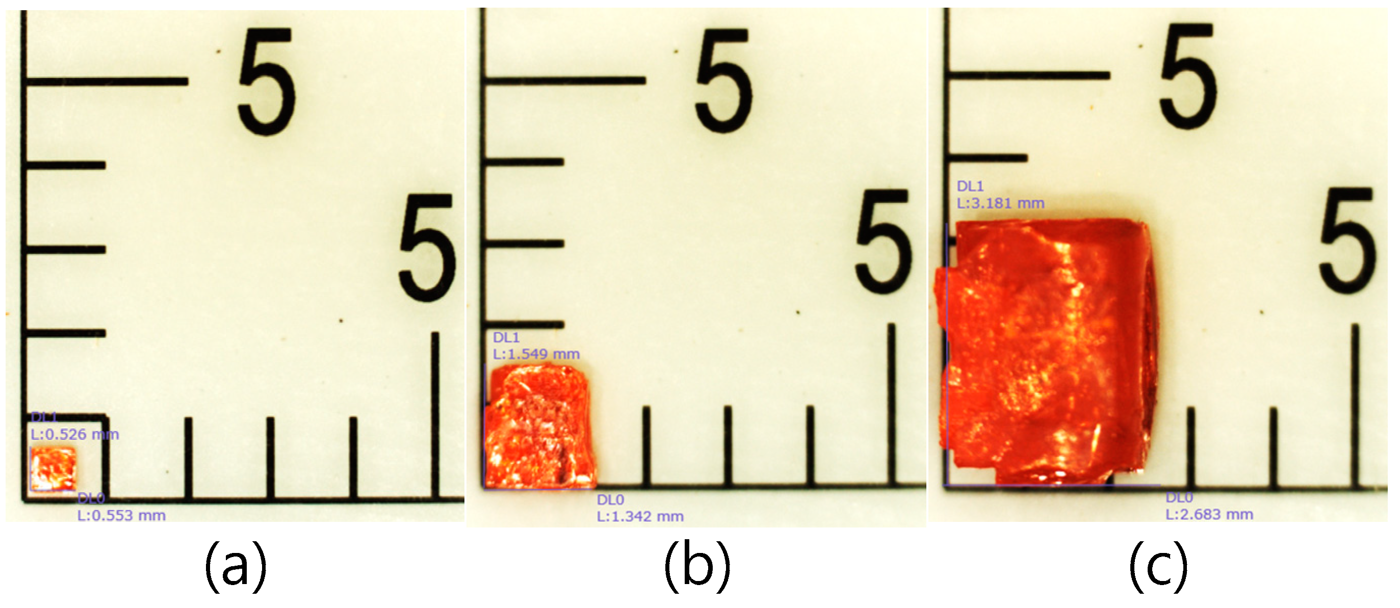
Figure 2 presents the images of the MAPbBr3 perovskite crystals grown by inverse temperature crystallization several times. The size of the crystal increased after multiple crystallization growth processes. The surface status was difficult to observe by the naked eye. The XRD patterns of all samples demonstrated s pure perovskite phase, as shown in Figure 3. One strong diffraction peak was located at 29.4°, which corresponds to the (200) perovskite plane, and was observed for the sample formed after the first growth cycle [19]. On the other hand, for the sample formed after the third growth cycle, we observed five main peaks, located at 29.56°, 33.23°, 42.56°, 44.67°, and 45.38°, which correspond to the (200), (210), (220), (300), and (310) perovskite planes, respectively. This sample exhibited poly-crystallization. The sample obtained after the first growth cycle is said to be the seed core. The seed core demonstrated a strongly preferred orientation. However, the crystal quality of the shell layer formed outside the seed core after multiple crystallization steps worsened. The average crystalline size (D) can be calculated from the full width at half maximum (FWHM) of the XRD peak using Scherrer’s equation [21].
where λ = 1.54 Å (X-ray diffractometer with Cu Kα radiation), β is the observed FWHM, θ is the diffraction angle of the (200) peaks, and k is a shape factor with a value of 1 for perovskite materials. The crystalline sizes were determined as 608, 415, and 91 nm, respectively, indicating that the crystalline sizes in the shell decreased after multiple crystallization growth.
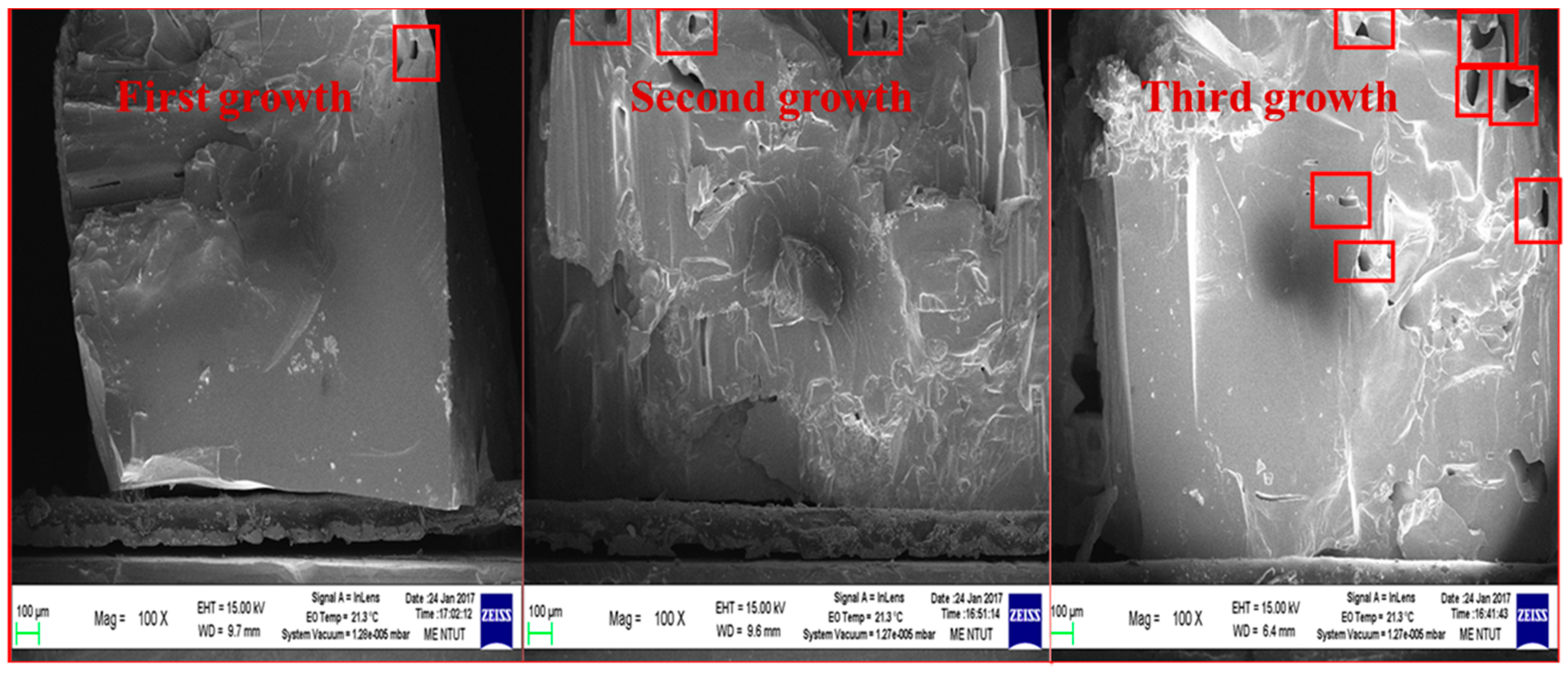
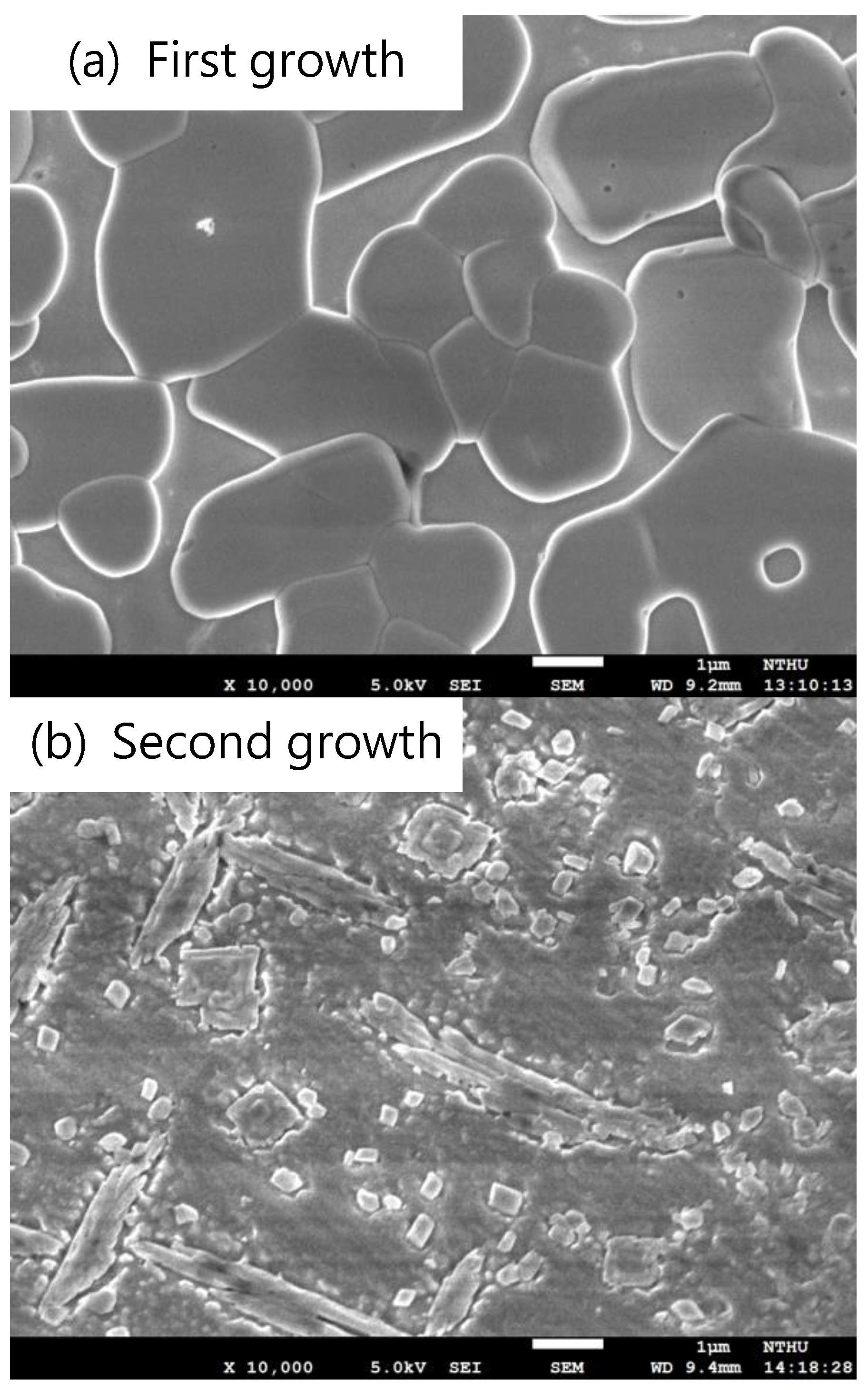
To investigate the surface morphologies of the resulting perovskite MAPbBr3 crystals, their SEM images were acquired. Typical SEM images of MAPbBr3 crystals grown by the multiple crystallization process are shown in Figure 4. There were many grain boundary lines in all samples. The grain size increased as the crystallization process time increased. Additionally, the samples after multiple growth cycles showed more voids on their surface. The void may be produced by crystal redissolution in the perovskite solution. Therefore, a longer reaction time in the perovskite solution led to more voids. Figure 5 shows high-resolution SEM of MAPbBr3 crystals grown by the multiple crystallization process. The sample for the first crystallization growth showed a smooth surface morphology with many interconnected grains, but a grain boundary line or dislocation could be seen in the samples after multiple crystallization processes, which is consistent with the XRD patterns observed. As the crystal size increased, the crystal quality worsened. This may be attributed to a fast deposition of the small MAPbBr3 grains to form the shell layer.
Figure 6 shows the room-temperature photoluminescence (PL) spectra of MAPbBr3 perovskite bulk crystals obtained with different growth times. The weak intensity of the PL spectrum for the sample of the first growth cycle is due to the crystal’s small size, which was smaller than the laser spot. The spectrum of the sample of the second growth cycle showed the strongest intensity owing to good crystal quality and large enough size. The PL spectra peaks located at 566, 570, and 575 nm for the first, second, and third crystallizations, respectively, matched the value reported in reference [18]. The PL spectrum peak located at 566 nm for the sample after the first growth cycle had the highest energy across all spectra. It originated from a band-to-band transition. The crystal size in the thin film is typically around tens of nanometers. When the crystal size was small, such as 0.5 mm × 0.5 mm (first growth cycle), the band gap value was 2.187 eV and, thus, close to 2.242 eV, which is the value for a thin film [22]. The band gap shifted toward 2.157 eV (third growth cycle) as the crystal size increased after multiple crystallizations. The lower energy peak at 575 nm (2.157 eV) may be attributed to the recombination of the deep level caused by the crystal voids at the surface [23].
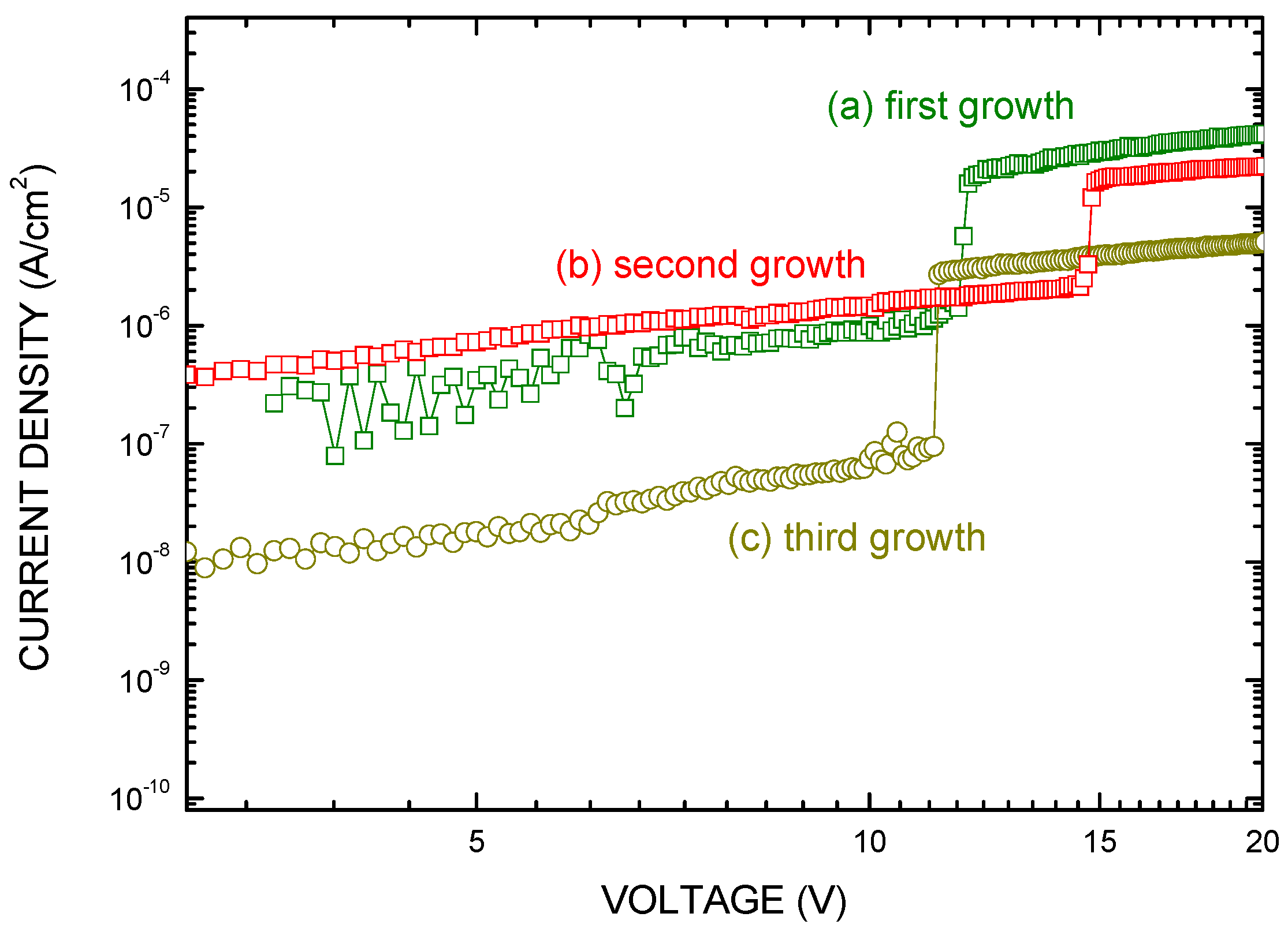
Figure 7 shows the dark current density–voltage (J–V) characteristics of MAPbBr3 crystals grown by multiple crystallization process. In a semiconductor, when the electric field applied between the electrodes is small, the injection current complies with Ohm’s law, and the current density–voltage characteristics are linear (J ∝ V). The applied bias range is in the ohmic region. When the applied electric field is high enough, the current is dominated by charge carriers injected from the contacts, and the current density–voltage characteristics become quadratic (J ∝ V2), i.e., follow Child’s law. The applied bias range is in the space-charge limited current (SCLC) region, or Child region. The transit region from ohmic to Child regions is the trap-filled limit (TFL) region. The SCLC current density can be expressed using the Mott–Gurney law:
where V is the applied voltage, J is the current density, L is the perovskite film thickness, A is the area, μ is the mobility, εr is the relative dielectric constant of MAPbBr3, (εr = 28.7, [24]), and ε0 is the vacuum permittivity. Therefore, the mobility in a semiconductor can be determined by its logarithmic current–voltage curve in the SCLC region. In order to know the carrier transporting characteristics in the MAPbBr3 crystals, we used the SCLC model to determine the carrier mobility [18]. Here, Ag was used for the electrodes in all samples. The mobilities for the samples after first, second, and third growth were calculated to be 0.9, 5.6, and 54.7 cm2/Vs, respectively. The mobility analysis showed a good match with previous single crystals grown at room temperature [18,19,20]. The higher mobility after multiple crystallization processes indicated that the surface states caused by voids in the crystals favored electron transition in the perovskite material. This is consistent with the observations of XRD and SEM and with some previous reports.
4. Conclusions
In conclusion, we demonstrated that the MAPbBr3 bulk crystals can be prepared by the repeated inverse temperature crystallization method. The XRD patterns of all samples demonstrated pure perovskite planes. One strong diffraction peak located at 29.4°, which corresponds to the (200) perovskite plane, was observed. However, there were five mean peaks located at 29.56°, 33.23°, 42.56°, 44.67°, and 45.38°, which correspond to the (200), (210), (220), (300), and (310) perovskite planes, respectively, after the third growth cycle. As the crystal size increased, the crystal planes changed from single crystallization to poly-crystallization after multiple crystallization processes. The crystal qualities worsened as the crystal size became bigger and bigger because of the strains caused by imperfections and distortion. Especially, in the third growth cycle, the quality rapidly decayed. The band gap shifted toward 2.157 eV (third growth cycle) after multiple crystallizations. This may be attributed to the recombination of deep levels caused by the surface states of the crystal voids. The mobilities for the samples after the first, second, and third crystallization processes were calculated to be 0.9, 5.6, and 54.7 cm2/Vs, respectively. The higher mobility after multiple crystallization processes indicated that the surface states caused by the voids in the crystals favored electron transition in the perovskite material. Therefore, the shell layer formed after the third growth cycle had a large number of voids due to fast deposition and exhibited a higher electron transition and strong emission from the deep level caused by the voids. It is our future work to find a way to grow a large MAPbBr3 single crystal.
Author Contributions
L.-C.C. wrote the paper, designed the experiments, and analyzed the data. K.-L.L. and S.-E.L. prepared the samples and performed all measurements. All authors read and approved the final manuscript.
Funding
Financial support for this paper was provided by the Ministry of Science and Technology of the Republic of China under contract no. MOST 106-2218-E-027-091.
Conflicts of Interest
The authors declare no conflict of interest.
References
- Xing, G.; Mathews, N.; Sun, S.; Lim, S.S.; Lam, Y.M.; Grätzel, M.; Mhaisalkar, S.; Sum, T.C. Long-Range Balanced Electron- and Hole-Transport Lengths in Organic-Inorganic CH3NH3PbI3. Science 2013, 342, 344–347. [Google Scholar] [CrossRef] [PubMed]
- Noh, J.H.; Im, S.H.; Heo, J.H.; Mandal, T.N.; Seok, S.I. Chemical Management for Colorful, Efficient, and Stable Inorganic–Organic Hybrid Nanostructured Solar Cells. Nano Lett. 2013, 13, 1764–1769. [Google Scholar] [CrossRef] [PubMed]
- Filip, M.R.; Eperon, G.E.; Snaith, H.J.; Giustino, F. Steric engineering of metal-halide perovskites with tunable optical band gaps. Nat. Commun. 2014, 5, 5757. [Google Scholar] [CrossRef] [PubMed] [Green Version]
- D’Innocenzo, V.; Kandada, A.R.S.; De Bastiani, M.; Gandini, M.; Petrozza, A. Tuning the Light Emission Properties by Band Gap Engineering in Hybrid Lead Halide Perovskite. J. Am. Chem. Soc. 2014, 136, 17730–17733. [Google Scholar] [CrossRef] [PubMed]
- Docampo, P.; Ball, J.M.; Darwich, M.; Eperon, G.E.; Snaith, H.J. Efficient organometal trihalide perovskite planar-heterojunction solar cells on flexible polymer substrates. Nat. Commun. 2013, 4, 2761. [Google Scholar] [CrossRef] [PubMed] [Green Version]
- Kim, H.S.; Mora-Sero, I.; Gonzalez-Pedro, V.; Fabregat-Santiago, F.; Juarez-Perez, E.J.; Park, N.G.; Bisquert, J. Mechanism of carrier accumulation in perovskite thin-absorber solar cells. Nat. Commun. 2013, 4, 2242. [Google Scholar] [CrossRef] [PubMed] [Green Version]
- Stranks, S.D.; Eperon, G.E.; Grancini, G.; Menelaou, C.; Alcocer, M.J.; Leijtens, T.; Herz, L.M.; Petrozza, A.; Snaith, H.J. Electron-Hole Diffusion Lengths Exceeding 1 Micrometer in an Organometal Trihalide Perovskite Absorber. Science 2013, 342, 341–344. [Google Scholar] [CrossRef] [PubMed]
- Mei, A.; Li, X.; Liu, L.; Ku, Z.; Liu, T.; Rong, Y.; Xu, M.; Hu, M.; Chen, J.; Yang, Y.; et al. A hole-conductor–free, fully printable mesoscopic perovskite solar cell with high stability. Science 2014, 345, 295–298. [Google Scholar] [CrossRef] [PubMed]
- Christians, J.A.; Fung, R.C.M.; Kamat, P.V. An Inorganic Hole Conductor for Organo-Lead Halide Perovskite Solar Cells. Improved Hole Conductivity with Copper Iodide. J. Am. Chem. Soc. 2014, 136, 758–764. [Google Scholar] [CrossRef] [PubMed]
- Liu, D.; Yang, J.; Kelly, T.L. Compact Layer Free Perovskite Solar Cells with 13.5% Efficiency. Am. J. Chem. Soc. 2014, 136, 17116–17122. [Google Scholar] [CrossRef] [PubMed]
- Nie, W.; Tsai, H.; Asadpour, R.; Blancon, J.C.; Neukirch, A.J.; Gupta, G.; Crochet, J.J.; Chhowalla, M.; Tretiak, S.; Alam, M.A.; et al. High-efficiency solution-processed perovskite solar cells with millimeter-scale grains. Science 2015, 347, 522–525. [Google Scholar] [CrossRef] [PubMed] [Green Version]
- Choi, J.J.; Yang, X.; Norman, Z.M.; Billinge, S.J.L.; Owen, J.S. Structure of Methylammonium Lead Iodide within Mesoporous Titanium Dioxide: Active Material in High-Performance Perovskite Solar Cells. Nano Lett. 2014, 14, 127–133. [Google Scholar] [CrossRef] [PubMed]
- Tan, Z.K.; Moghaddam, R.S.; Lai, M.L.; Docampo, P.; Higler, R.; Deschler, F.; Price, M.; Sadhanala, A.; Pazos, L.M.; Credgington, D.; et al. Bright light-emitting diodes based on organometal halide perovskite. Nat. Nano 2014, 9, 687–692. [Google Scholar] [CrossRef] [PubMed]
- Dou, L.; Yang, Y.M.; You, J.; Hong, Z.; Chang, W.H.; Li, G.; Yang, Y. Solution-processed hybrid perovskite photodetectors with high detectivity. Nat. Commun. 2014, 5, 5404. [Google Scholar] [CrossRef] [PubMed] [Green Version]
- Pathak, S.; Sakai, N.; Rivarola, F.W.R.; Stranks, S.D.; Liu, J.; Eperon, G.E.; Ducati, C.; Wojciechowski, K.; Griffiths, J.T.; Haghighirad, A.A.; et al. Perovskite Crystals for Tunable White Light Emission. Chem. Mater. 2015, 27, 8066–8075. [Google Scholar] [CrossRef]
- Xing, G.; Mathews, N.; Lim, S.S.; Yantara, N.; Liu, X.; Sabba, D.; Grätzel, M.; Mhaisalkar, S.; Sum, T.C. Low-temperature solution-processed wavelength-tunable perovskites for lasing. Nat. Mater. 2014, 13, 476–480. [Google Scholar] [CrossRef] [PubMed]
- Chen, Y.-S.; Manser, J.S.; Kamat, P.V. All Solution-Processed Lead Halide Perovskite-BiVO4 Tandem Assembly for Photolytic Solar Fuels Production. J. Am. Chem. Soc. 2015, 137, 974–981. [Google Scholar] [CrossRef] [PubMed]
- Saidaminov, M.I.; Abdelhady, A.L.; Murali, B.; Alarousu, E.; Burlakov, V.M.; Peng, W.; Dursun, I.; Wang, L.; He, Y.; Maculan, G.; et al. High-quality bulk hybrid perovskite single crystals within minutes by inverse temperature crystallization. Nat. Commun. 2015, 6, 7586. [Google Scholar] [CrossRef] [PubMed] [Green Version]
- Shi, D.; Adinolfi, V.; Comin, R.; Yuan, M.; Alarousu, E.; Buin, A.; Chen, Y.; Hoogland, S.; Rothenberger, A.; Katsiev, K.; et al. Low trap-strate density and long carrier diffusion in organolead trihalide perovskite single crystals. Science 2015, 347, 519–522. [Google Scholar] [CrossRef] [PubMed]
- Maculan, G.; Sheikh, A.D.; Abdelhady, A.L.; Saidaminov, M.I.; Haque, M.A.; Murali, B.; Alarousu, E.; Mohammed, O.F.; Wu, T.; Bakr, O.M. CH3NH3PbCl3 Single Crystals: Inverse Temperature Crystallization and Visible-Blind UV-Photodetector. J. Phys. Chem. Lett. 2015, 6, 3781–3786. [Google Scholar] [CrossRef] [PubMed]
- Zhang, Z.; Wang, C.-C.; Zakaria, R.; Ying, J.Y. Role of Particle Size in Nanocrystalline TiO2-Based Photocatalysts. J. Phys. Chem. B 1998, 102, 10871–10878. [Google Scholar] [CrossRef]
- Chen, L.-C.; Wu, J.-R.; Tseng, Z.-L.; Chen, C.-C.; Chang, S.H.; Huang, J.-K.; Lee, K.-L.; Cheng, H.-M. Annealing Effect on (FAPbI3)1−x(MAPbBr3)x Perovskite Films in Inverted-Type Perovskite Solar Cells. Materials 2016, 9, 747. [Google Scholar] [CrossRef] [PubMed]
- Wang, K.-H.; Li, L.-C.; Shellaiah, M.; Sun, K.W. Structural and Photophysical Properties of Methylammonium Lead Tribromide (MAPbBr3) Single Crystals. Sci. Rep. 2017, 7, 13643. [Google Scholar] [CrossRef] [PubMed]
- Onoda-Yamamuro, N.; Matsuo, T.; Suga, H. Dielectric study of CH3NH3PbX3 (X = Cl, Br, I). J. Phys. Chem. Solids 1992, 53, 935–939. [Google Scholar] [CrossRef]
Figure 1.
Preparation of the MAPbBr3 perovskite crystals.

Figure 2.
Photo images for MAPbBr3 bulks after (a) first; (b) second; (c) third crystallization.

Figure 3.
XRD pattern of MAPbBr3 bulk crystal formed after the first, second, and third crystallization processes.
Figure 3.
XRD pattern of MAPbBr3 bulk crystal formed after the first, second, and third crystallization processes.

Figure 4.
Low-magnification SEM images for MAPbBr3 bulks after the first, second, and third crystallization process.
Figure 4.
Low-magnification SEM images for MAPbBr3 bulks after the first, second, and third crystallization process.

Figure 5.
High-magnification SEM images for MAPbBr3 bulks after the first, second, and third crystallization process.
Figure 5.
High-magnification SEM images for MAPbBr3 bulks after the first, second, and third crystallization process.


Figure 6.
Photoluminescence (PL) spectra of MAPbBr3 bulk crystals after the first, second, and third crystallization process.
Figure 6.
Photoluminescence (PL) spectra of MAPbBr3 bulk crystals after the first, second, and third crystallization process.

Figure 7.
Dark current density–voltage (J–V) curves for MAPbBr3 bulks after the (a) first; (b) second; (c) third crystallization processes.
Figure 7.
Dark current density–voltage (J–V) curves for MAPbBr3 bulks after the (a) first; (b) second; (c) third crystallization processes.

© 2018 by the authors. Licensee MDPI, Basel, Switzerland. This article is an open access article distributed under the terms and conditions of the Creative Commons Attribution (CC BY) license (http://creativecommons.org/licenses/by/4.0/).
Share and Cite
MDPI and ACS Style
Chen, L.-C.; Lee, K.-L.; Lin, S.-E. Observation of Hybrid MAPbBr3 Perovskite Bulk Crystals Grown by Repeated Crystallizations. Crystals 2018, 8, 260. https://doi.org/10.3390/cryst8070260
AMA Style
Chen L-C, Lee K-L, Lin S-E. Observation of Hybrid MAPbBr3 Perovskite Bulk Crystals Grown by Repeated Crystallizations. Crystals. 2018; 8(7):260. https://doi.org/10.3390/cryst8070260
Chicago/Turabian StyleChen, Lung-Chien, Kuan-Lin Lee, and Shao-En Lin. 2018. "Observation of Hybrid MAPbBr3 Perovskite Bulk Crystals Grown by Repeated Crystallizations" Crystals 8, no. 7: 260. https://doi.org/10.3390/cryst8070260
Note that from the first issue of 2016, this journal uses article numbers instead of page numbers. See further details here.