Article

Analysis of Switching Current Data during Polarization Reversal in KTP Single Crystals with Surface Dielectric Layer

School of Natural Sciences and Mathematics, Ural Federal University, Ekaterinburg 620000, Russia
*
Author to whom correspondence should be addressed.
Crystals 2018, 8(8), 315; https://doi.org/10.3390/cryst8080315
Submission received: 27 June 2018 / Revised: 26 July 2018 / Accepted: 2 August 2018 / Published: 4 August 2018
(This article belongs to the Special Issue KTP Crystal for Nonlinear Optical and Electrooptic Applications)

Abstract

:
Studies of polarization reversal processes in potassium titanyl phosphate (KTiOPO4, KTP) single crystals with surface dielectric layer are important due to their potential applications as the basis of bottom-up technology for creation of periodically poled nonlinear-optical crystals. We present the results of switching currents analysis accompanied by in situ visualization of domain kinetics during polarization reversal in KTP with 3 m-thick photoresist dielectric layer. Qualitative change of the switching current shape has been revealed as compared to the polarization reversal without surface dielectric layer. Two stages of domain structure evolution have been distinguished by in situ visualization of domain kinetics. The formation of submicron domain streamers in front of the moving domain walls has been revealed. The broadening of the domain streamers (1D domain growth) was observed at the second stage. The switching currents were approximated by the modified Kolmogorov-Avrami formula taking into account the change of the growth dimensionality (“geometrical catastrophe”). The sufficient input of the 1D growth to the switching process decreased with increase of the switching field. The obtained results were attributed to the domain wall shape instability induced by retardation of the depolarization field screening in ferroelectric with surface dielectric layer.

1. Introduction

The first synthesis of potassium titanyl phosphate (KTiOPO4, KTP) single crystals was realized in the 1970s [1,2] and was followed by active studies of ferroelectric properties in the 1980s [3]. Bierlein et al. have carried out the first polarization reversal of KTP crystals at elevated temperatures [4]. Later, the dependences of the main parameters of the dielectric hysteresis loops (spontaneous polarization and coercive fields) on temperature and deviation from the stoichiometric composition and field dependence of the switching time were studied [5,6,7]. It should be noted that the KTP single crystals family with various potassium content demonstrating a strong variation of the bulk conductivity from 10−12 to 10−8 Ohm−1 cm−1.
Considerable attention was paid to the periodical poling in KTP. As a result, even the submicron domain periods have been achieved [8,9]. Currently, the periodically poled KTP crystals are among the popular materials for nonlinear optical applications including optical parametric oscillation [10,11,12] and second harmonic generation [13,14,15,16,17]. The precise periodical poling in KTP requires deep knowledge of the domain structure evolution including the switching time and switching current statistics [18].
The pursuit of the unusual low-dimensional processes and study of their evolution is at the very core of condensed matter physics. In particular, discovering the self-organized formation and growth of oriented domain rays in uniaxial ferroelectrics during polarization reversal in highly-nonequilibrium conditions [19,20] has become a significant step in this endeavor due to rich physical phenomena and strong technological promise of bottom-up periodical domain structures creation. Although there have been significant efforts in the study of these processes in lithium niobate and lithium tantalate single crystals their applicability could be elusive due to the C3v symmetry and inherent three preferred domain wall orientations. From this point of view, the KTP crystals possessing the C2v symmetry emerge as the best materials for studying the 1D domain growth processes with potential applications in periodical poling.
The important condition for transition from the conventional domain wall motion to the oriented domain rays formation is the realization of highly-nonequilibrium switching conditions which are tightly related with the screening ineffectiveness of depolarization field. Among other methods the technologically available creation of the artificial dielectric layer provides effective control of the screening ineffectiveness [19,21,22].
The experimental study of polarization reversal in ferroelectrics is based on two groups of methods: local and integral [23,24]. The local methods representing the in situ visualization of domain kinetics providing the detailed and direct information about the domain structure evolution lacks high enough temporal and spatial resolution. On the other hand, the integral methods including the switching current measurement demonstrate better temporal resolution and easier realization, but the adequate analysis of experimental data requires the additional information for choosing the proper model [25]. The combined approach of local and integral methods allows choosing the model for analysis of switching current data in terms of Kolmogorov-Avrami (K-A) approach with high temporal resolution [23,24,26].
The K-A approach initially proposed for metal crystallization from the melt [27,28] was applied by Ishibashi and Takagi for analysis of the switching currents in ferroelectrics [29]. Shur and Rumyantsev have modified the K-A formula for polarization reversal in the finite media taking into account the abrupt changes of the growth dimensionality (“geometrical catastrophe”) [23,25,26].
In this paper, we have studied the 1D domain growth processes realized during the polarization reversal in KTP single crystals with surface dielectric layer by analysis of the switching current data in terms of a modified Kolmogorov-Avrami approach [25].

2. Materials and Methods

The crystals under investigation were grown by top-seeded solution method (Novosibirsk, Russia). The studied samples represented 1 mm-thick z-cut optical grade polished plates with typical sizes 11 × 16 mm2. The bulk electrical conductivity at room temperature was about 3 × 10⁻⁹ Ohm−1 cm−1. It is known that the conductivity of KTP crystals decreases with increasing of the potassium content, which is between high and intermediate values in the studied samples [5].
The SM 180 spin coater (Sawatec, Sax, Switzerland) was used for deposition of the artificial dielectric layer of negative photoresist (AZ nlof2020, Microchemicals, Ulm, Germany) on Z+ polar surface. The coating parameters were taken according to the photoresist datasheets. After the deposition the flood exposure using MJB4 Mask Aligner (SUSS MicroTec, Garching, Germany) was performed by i-line of Hg light source with 180 mW·cm−2 irradiation dose. All photoresist films were hard-baked at temperature 110 °C for 5 min with cooling/heating rate below 5 °C/min. The photoresist films thickness of 3.1 μm was measured by Wyko NT 1100 optical profilometer (Veeco, New York, NY, USA) and scanning probe microscope NTEGRA Aura (NT-MDT, Zelenograd, Russia). The dielectric constant of the obtained layer was about 7 [30].
Liquid 2 mm diameter electrodes of the saturated LiCl aqueous solution formed in the sample fixture made from Plexiglas with silicone rubber pads were used for polarization reversal. The voltage pulses of arbitrary shape generated by multifunctional data acquisition board NI PCI-6251 (National Instruments, Austin, TX, USA) and amplified by high voltage amplifier TREK 20/20 C (Trek Inc., New York, NY, USA) were applied to the sample. The rectangular external field pulses were used for forward polarization reversal in constant electric field with duration ranging from 1 to 15 s, field amplitude ranging from 4.6 to 5.8 kV/mm and field rise time 0.1 s. The rectangular field pulse of reverse polarity with amplitude 4.5 kV/mm was applied after each forward polarization reversal. The chosen pulse duration was more than four times longer the switching time to ensure the single domain state for the following forward polarization reversal. Moreover, the 15 min interval was maintained between the reverse and the forward field pulses for complete sample relaxation to the initial state [31]. The switching time was defined as a time interval corresponding to the 0.95 of the total switched charge, which was acquired by the integration of the switching current data. The obtained switched charge during the field rise time was below 0.05 from the total one for the highest applied field 5.8 kV/mm. Therefore, we neglected the effect of rise time during current analysis.

3. Results

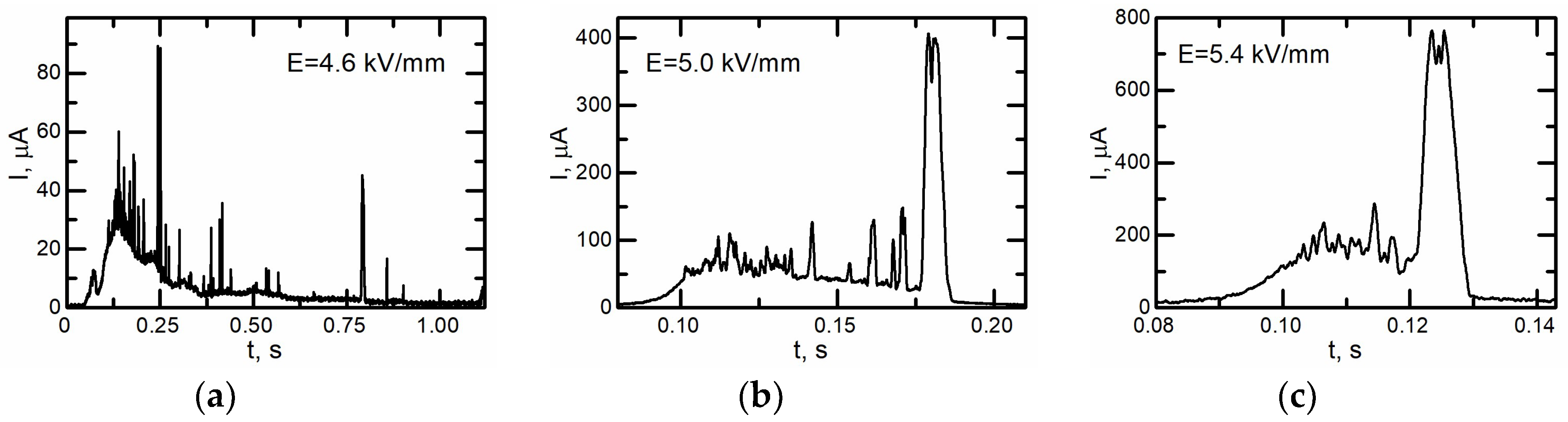
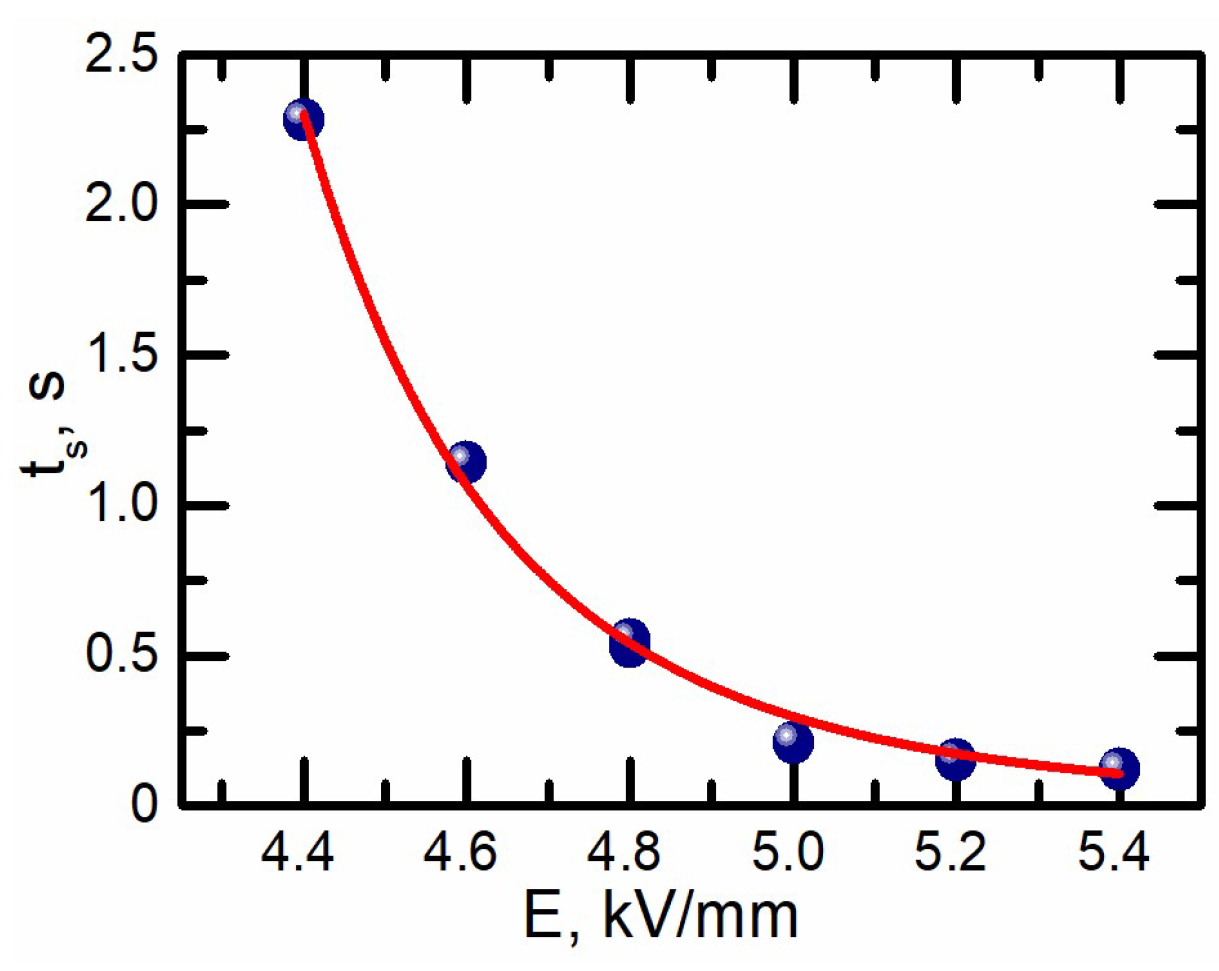
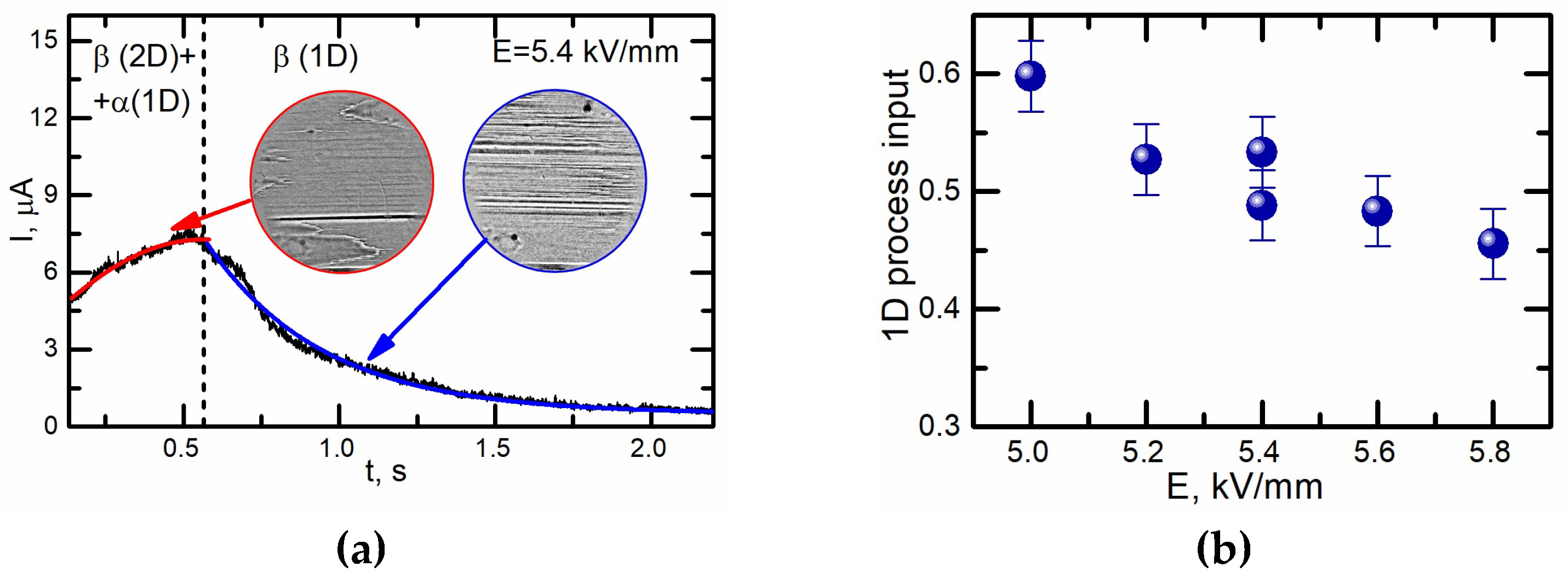
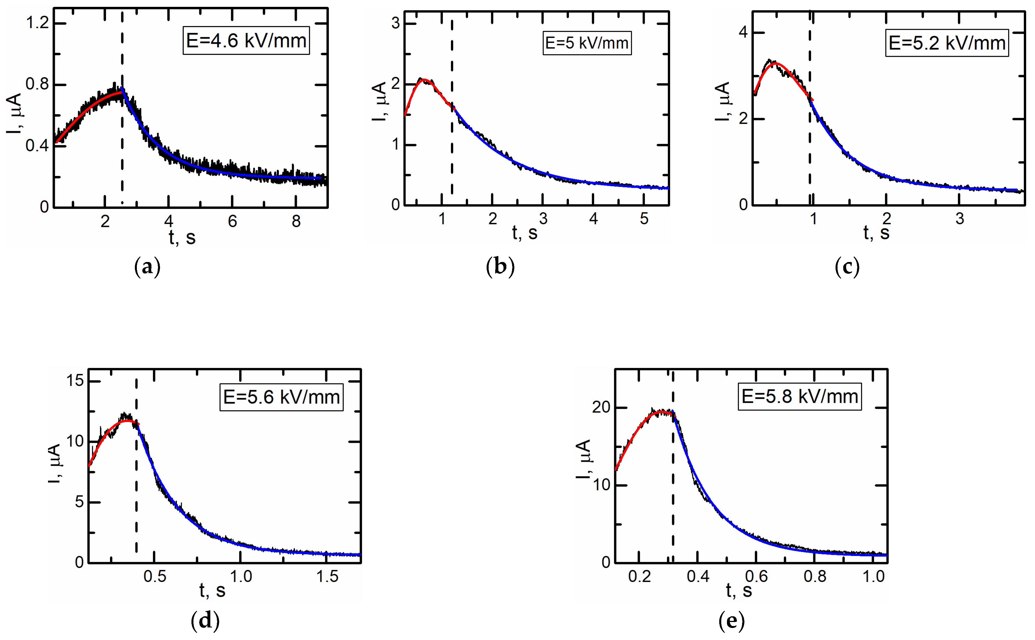
3.1. Polarization Reversal without Artificial Dielectric Layer

Switching currents during the polarization reversal of KTP samples without artificial surface dielectric layer possessed the smooth shape with strong oscillations (Figure 1). Such type of current shape was previously reported and analyzed [31].
According to the in situ domain kinetics observation the current peaks corresponded to the domain wall jumps after merging events [31,32] (Figure 2). The higher threshold fields obtained in the present paper as compared to [31] can be attributed to slight difference of the crystal composition [5].
The dependence of the switching time ts on applied field obtained from the analysis of switching current data followed the activation-type dependence (Figure 3):
  t s = t 0 · exp ( E a c E E b )  
where Eac is activation field, E is external field, Eb is bias field, and t0 is switching time in the limit of high fields.
The fitting of the experimental data by Equation (1) allowed obtaining the activation and bias fields for polarization reversal of KTP without artificial dielectric layer: Eac = (34.0 ± 1.2) kV/mm and Eb = (1.5 ± 0.2) kV/mm.

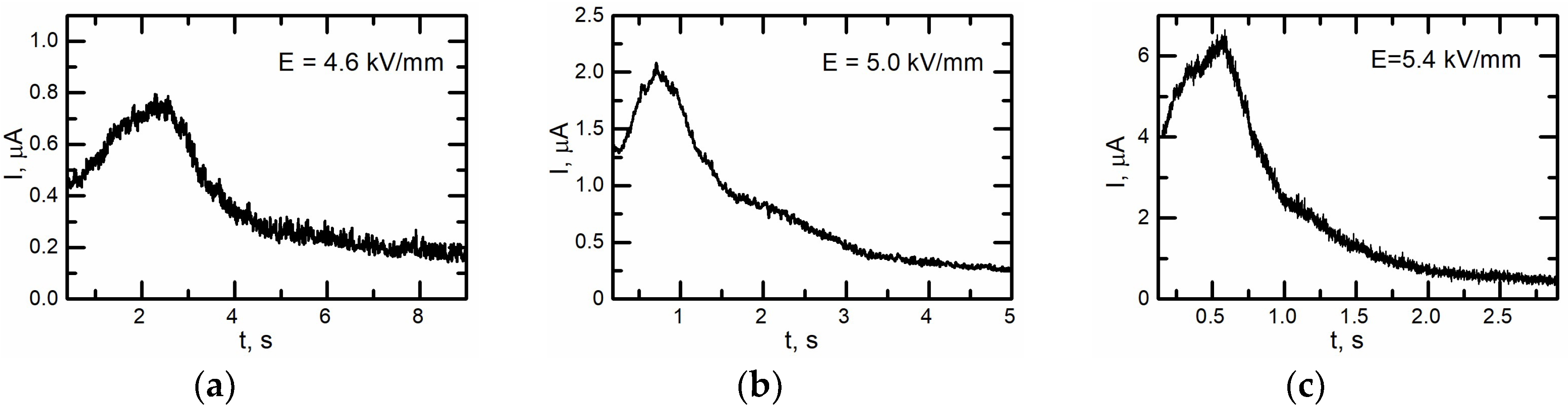
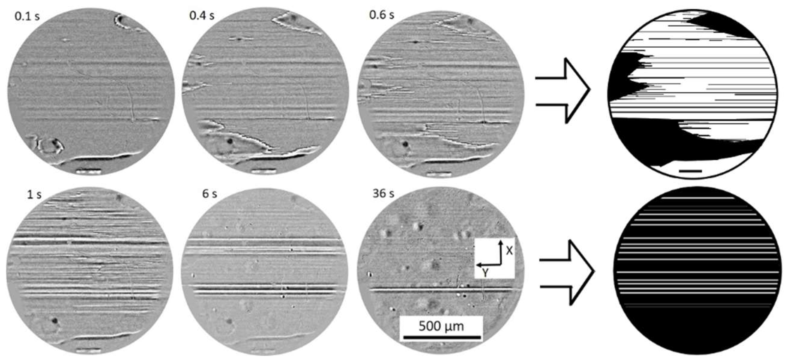
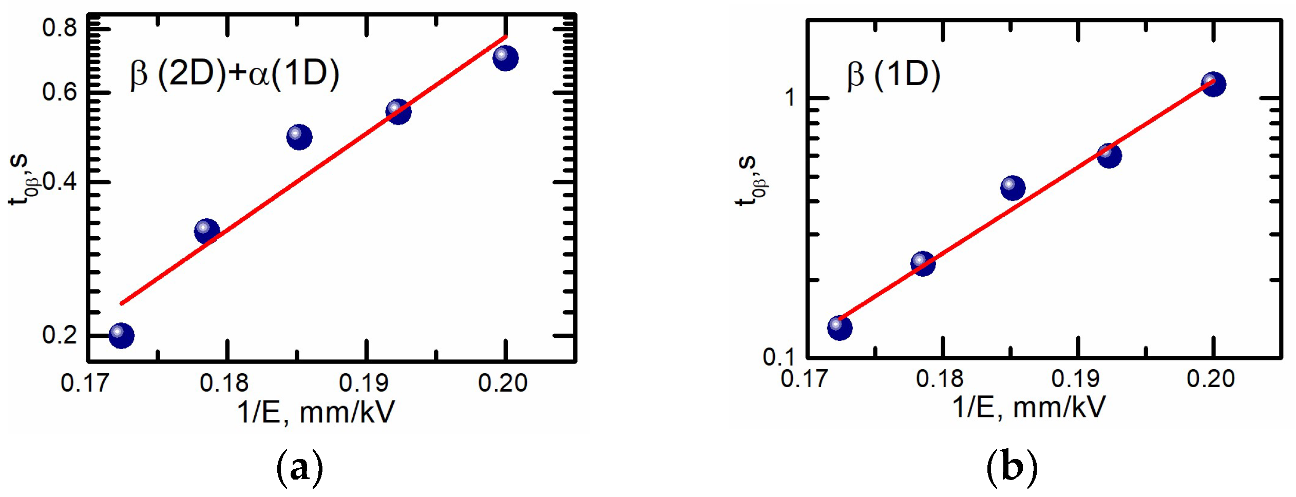
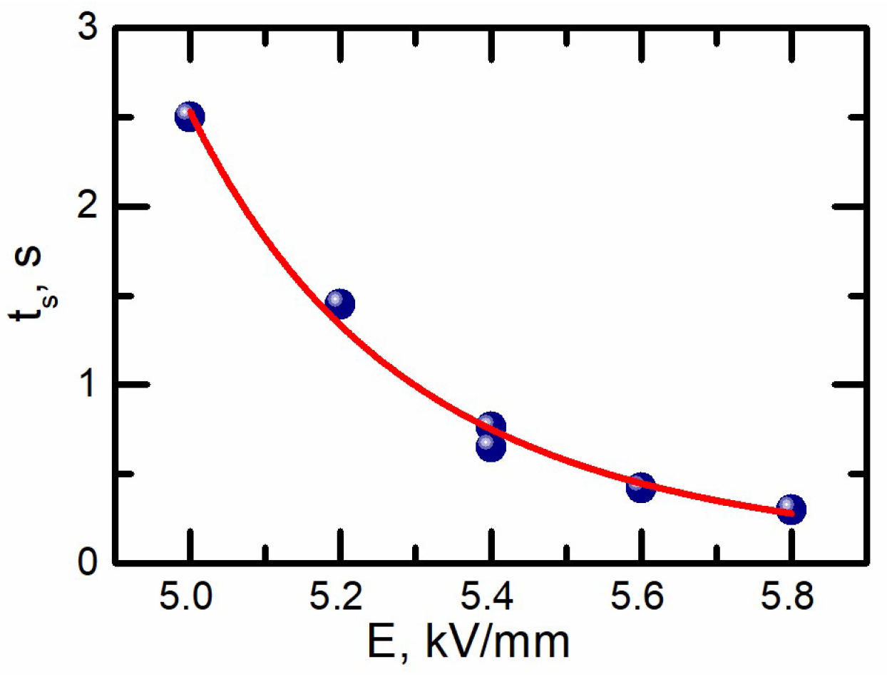
3.2. Polarization Reversal with Artificial Dielectric Layer

The polarization reversal with artificial dielectric layer led to qualitative change of the switching current shape. The smooth current without oscillations was observed for the whole range of applied fields (Figure 4). Such current shape usually corresponds to the smooth growth of a large number of individual isolated domains without any domain wall jumps [33,34].
The in situ visualization of the domain structure during polarization reversal by optical microscopy allowed revealing two stages of domain structure evolution. First, growth of macroscopic domain walls accompanied by formation of the domain rays (“streamers”) oriented along Y crystallographic direction of submicron width in front of the moving walls (Figure 5). Second, disappearance of macroscopic domain walls by reaching of the opposite electrode edge and complete decay of the domain structure to individual streamers.
The polarization reversal at the stage after geometrical catastrophe occurred by the sideways motion of streamer’s domain walls in X crystallographic direction (streamers broadening) representing 1D process. The jump-like motion of domain walls is fully suppressed. The detailed study of streamer kinetics by local methods will be published by us elsewhere.
The visualization of the domain structure after partial polarization reversal by piezoresponse force microscopy (PFM) has shown that the streamer width ranged from 0.5 to 2 μm (Figure 6).
Taking in account the results of in situ visualization domain kinetics we have analyzed the shape of switching current using the modified K-A approach. The process of polarization reversal was divided into two stages. The first represents the growth of macroscopic domains with formation and growth of domain streamers and corresponds to the β(2D) + α(1D) process within the K-A model. The second represents the predominate broadening of the domain streamers and corresponds to the β(1D)-process within the K-A model. The switching current data were approximated by the following expression:
  j ( t ) = { 2 P s A 2 t 0 α t t s t t 0 α e x p ( ( t t s t t 0 α ) 2 ( 1 t t m ) ) ,   f o r   t   t c a t 2 P s A 1 t 0 β e x p ( t t s t t 0 β ) ,                                                                     f o r   t   t c a t  
where PS is the spontaneous polarization, A is the switched area, tst is the time of switching process start, t0a and t are characteristic times of corresponding stages, tcat is the time of geometrical catastrophe, and tm accounts for growing domain achievement of the switched area boundaries.
As the α (1D)-process has the same exponent in the switching current expression as β (2D) process, the switching current corresponding to β (2D) + α (1D) process was fitted by single formula (Equation (2)). The fitting of the whole current data by Equation (2) with tcat as a free parameter allowed to reveal its value. The adequate accuracy of this method has been confirmed by analysis of the domain structure corresponding to the catastrophe time obtained by fitting.
The example of switching current fitting is presented at Figure 7a. The revealed unusual strong input of the 1D process corresponded to about the half of the whole switched charge. It was shown that the input of the 1D process decreases with field increase from about 0.6 for 5 kV/mm to 0.45 for 5.8 kV/mm (Figure 7b). This fact indicates that the domain streamers growth is more pronounced for fields just above the threshold value. It is clear that the switching current during the second stage decreases only. Therefore, the time of geometrical catastrophe corresponding to transition from the β(2D) + α(1D) process to the β(1D) one is located close to the middle of the switching process.
The switching currents for other external fields fitted by Equation (2) are presented in Figure 8.
The characteristic times of the β(2D) + α(1D) and β(1D) processes obtained from the fitting of the switching current data followed the activation type field dependences (Figure 9).
The characteristic times for field 4.6 kV/mm were not taken into account because the complete polarization reversal under the electrode area was not achieved in this case, even for field application for 2 minutes. This effect can be attributed to low nucleation density of streamers and motion velocity of macroscopic domain walls in low fields.
The obtained field dependences of characteristic times have been fitted by the equation:
  t 0 β ( E ) = t 1 · exp ( E a c β E )  
where Eac is activation field for corresponding process and t1 is the switching time in the limit of high fields.
Such analysis allowed extracting of the activation fields equal to (18 ± 2) kV/mm for β(2D) + α(1D) process and (35 ± 2) kV/mm for β(1D) process.
The activation-type field dependence of the switching time was obtained by analysis of the switching current data for various fields (Figure 10). The fitting of experimental data by Equation (1) allowed extracting the activation field equal to (41 ± 2) kV/mm and bias field equal to (1.5 ± 0.2) kV/mm.

4. Discussion

The obtained formation of domain streamers can be explained within the kinetic approach to the domain structure evolution taking into account the retardation of depolarization field screening in the bulk ferroelectrics with artificial surface dielectric layer [21,22]. The macroscopic domain wall motion decelerates due to the formation of the trail of partially compensated bound charges behind the moving domain wall [35,36]. It was shown by us experimentally in lithium niobate crystals that effect of the domain shape instability (formation of the quasi-periodical perturbations of the domain wall shape) is the most pronounced for values of the applied field just above the threshold ones [37]. The effect is stimulated by the residual depolarization field appeared due to retardation of the bulk screening of depolarization field. This field decelerates the sideways motion of the flat domain walls and induces the fast growth of perturbations along the wall leading to formation of fingers and streamers. It is clear that the effect appeared when the excess of the applied field over the threshold value is comparable with the residual depolarization field [38]. Therefore the input of the streamers to the switching process increased with field decrease.
Higher activation field for field dependence of the switching time in the sample with surface dielectric layer is also related to the increase of the residual depolarization field decelerating the motion of macroscopic walls.
It should be noted that the “bias field” in Equation (1) is just a parameter, which is somehow related to the internal fields in the crystal. Therefore, the equal values of Eb parameter can’t be interpreted as an evidence for the same values of internal bulk screening fields and bulk screening efficiency in the sample with and without the artificial dielectric layer. The real values of bulk screening fields can be measured and compared using the method of cyclic switching with varied delay time between forward and reverse switching [39,40].
The obtained knowledge allows separating the formation and growth of submicron stripe domains (streamers) by simple analysis of the switching current data. The studied effect has two implications for poling with submicron periods in KTP crystals. First, the self-organized creation of quasi-periodic domain structures for nonlinear frequency conversion without patterned periodical electrodes. Second, the estimation of the optimal parameters of electric field pulse for conventional electric-field poling. In this case, the field is applied through the periodical stripe windows in the photoresist layer. The domain broadening outside the electrodes leading to formation of the domain streamers can be easily detected by the analysis of the switching current shape as it was shown in the present paper. Thus, the proposed approach will be used for optimization of the periodical poling in KTP on the way to creation of sub-micron domain structures desired for frequency converters and electro-optic modulators with enhanced characteristics [41].

Author Contributions

Conceptualization, V.S. and A.A.; Methodology, A.A.; Investigation, E.V. and E.G.; Formal Analysis, E.V. and A.A.; Writing and Original Draft Preparation, A.A. and V.S.; Supervision, V.S.; Project Administration, A.A.

Funding

This research was made possible in part by the Government of the Russian Federation (Act 211, Agreement No. 02. A03.21.0006), by RFBR (Grant No. 16-02-00724) and by President of Russian Federation Grant for young scientists (Contract No. 14.Y30.17.2837-MK). V.S. and A.A. acknowledge financial support within the State Task from the Ministry of Education and Science of the Russian Federation (Project No. 1366.2014/236 and Contract No. 3.4973.2017/7.8).

Acknowledgments

The equipment of the Ural Center for Shared Use “Modern Nanotechnology” was used.

Conflicts of Interest

The authors declare no conflict of interest.

References

  1. Tordjman, I.; Masse, R.; Guitel, J.C. Structure cristalline du monophosphate KTiPO5. Zeitschrift Für Kristallographie-Cryst. Mater. 1974, 139, 103–115. [Google Scholar] [CrossRef]
  2. Zumsteg, F.C.; Bierlein, J.D.; Gier, E.T. KxRb1−xTiOPO4: A new nonlinear optical material. J. Appl. Phys. 1976, 47, 4980–4985. [Google Scholar] [CrossRef]
  3. Yanovskii, V.K.; Voronkova, V.I. Ferroelectric phase transitions and properties of crystals of the KTiOPO4 family. Phys. Status Solidi 1986, 93, 665–668. [Google Scholar] [CrossRef]
  4. Bierlein, J.D.; Ahmed, F. Observation and poling of ferroelectric domains in KTiOPO4. Appl. Phys. Lett. 1987, 51, 1322–1324. [Google Scholar] [CrossRef]
  5. Rosenman, G.; Urenski, P.; Arie, A.; Roth, M.; Angert, N.; Skliar, A.; Tseitlin, M. Polarization reversal and domain grating in flux-grown KTiOPO4 crystals with variable potassium stoichiometry. Appl. Phys. Lett. 2000, 76, 3798–3800. [Google Scholar] [CrossRef]
  6. Urenski, P.; Rosenman, G.; Molotskii, M. Polarization reversal and domain anisotropy in flux-grown KTiOPO4 and isomorphic crystals. J. Mater. Res. 2001, 16, 1493–1499. [Google Scholar] [CrossRef]
  7. Canalias, C.; Hirohashi, J.; Pasiskevicius, V.; Laurell, F. Polarization-switching characteristics of flux-grown KTiOPO4 and RbTiOPO4 at room temperature. J. Appl. Phys. 2005, 97, 124105. [Google Scholar] [CrossRef]
  8. Canalias, C.; Pasiskevicius, V. Mirrorless optical parametric oscillator. Nat. Photonics 2007, 1, 459–462. [Google Scholar] [CrossRef]
  9. Canalias, C.; Pasiskevicius, V.; Fokine, M.; Laurell, F. Backward quasi-phase-matched second-harmonic generation in submicrometer periodically poled flux-grown KTiOPO4. Appl. Phys. Lett. 2005, 86, 181105. [Google Scholar] [CrossRef]
  10. Chuchumishev, D.; Marchev, G.; Buchvarov, I.; Pasiskevicius, V.; Laurell, F.; Petrov, V. High-energy picosecond OPO based on PPKTP. Laser Phys. 2013, 10, 115404. [Google Scholar] [CrossRef] [PubMed] [Green Version]
  11. Marchev, G.; Dallocchio, P.; Pirzio, F.; Agnesi, A.; Reali, G.; Petrov, V.; Tyazhev, A.; Pasiskevicius, V.; Thilmann, N.; Laurell, F. Sub-nanosecond, 1–10 kHz, low-threshold, non-critical OPOs based on periodically poled KTP crystal pumped at 1.064 nm. Appl. Phys. B 2012, 109, 211–214. [Google Scholar] [CrossRef]
  12. Chaitanya Kumar, S.; Das, R.; Samanta, G.K.; Ebrahim-Zadeh, M. Optimally-output-coupled, 17.5 W, fiber-laser-pumped continuous-wave optical parametric oscillator. Appl. Phys. B 2010, 102, 31–35. [Google Scholar] [CrossRef]
  13. Canalias, C.; Pasiskevicius, V.; Laurell, F. Periodic poling of KTiOPO4: From micrometer to sub-micrometer domain gratings. Ferroelectrics 2006, 340, 27–47. [Google Scholar] [CrossRef]
  14. Mu, X.; Zotova, I.B.; Ding, Y.J.; Risk, W.P. Backward second-harmonic generation in submicron-period ion-exchanged KTiOPO4 waveguide. Opt. Commun. 2000, 181, 153–159. [Google Scholar] [CrossRef]
  15. Gu, X.; Makarov, M.; Ding, Y.J.; Khurgin, J.B.; Risk, W.P. Backward second-harmonic and third-harmonic generation in a periodically poled potassium titanyl phosphate waveguide. Opt. Lett. 1999, 24, 127–129. [Google Scholar] [CrossRef] [PubMed]
  16. Arie, A.; Rosenman, G.; Mahal, V.; Skliar, A.; Oron, M.; Katz, M.; Eger, D. Green and ultraviolet quasi-phase-matched second harmonic generation in bulk periodically-poled KTiOPO4. Opt. Commun. 1997, 142, 265–268. [Google Scholar] [CrossRef]
  17. Karlsson, H.; Laurell, F.; Cheng, L.K. Periodic poling of RbTiOPO4 for quasi-phase matched blue light generation. Appl. Phys. Lett. 1999, 74, 1519–1521. [Google Scholar] [CrossRef]
  18. Shur, V.Y.; Pelegova, E.V.; Akhmatkhanov, A.R.; Baturin, I.S. Periodically poled crystals of KTP family: A review. Ferroelectrics 2016, 496, 49–69. [Google Scholar] [CrossRef]
  19. Shur, V.Y.; Akhmatkhanov, A.R.; Chuvakova, M.A.; Dolbilov, M.A.; Zelenovskiy, P.S.; Lobov, A.I. Formation of self-organized domain structures with charged domain walls in lithium niobate with surface layer modified by proton exchange. J. Appl. Phys. 2017, 121, 104101. [Google Scholar] [CrossRef]
  20. Shur, V.Y.; Neradovskiy, M.M.; Dolbilov, M.A.; Lobov, A.I.; Zelenovskiy, P.S.; Ushakov, A.D.; Ushakova, E.S.; Quillier, E.; Baldi, P.; De Micheli, M.P. Formation of broad domain boundary in congruent lithium niobate modified by proton exchange. Ferroelectrics 2015, 476, 146–155. [Google Scholar] [CrossRef]
  21. Dolbilov, M.A.; Shur, V.Y.; Shishkina, E.V.; Angudovich, E.S.; Ushakov, A.D.; Baldi, P.; de Micheli, M.P. Formation of nanodomain structure in front of the moving domain wall in lithium niobate single crystal modified by proton exchange. Ferroelectrics 2013, 442, 82–91. [Google Scholar] [CrossRef]
  22. Akhmatkhanov, A.R.; Shur, V.Y.; Baturin, I.S.; Zorikhin, D.V.; Lukmanova, A.M.; Zelenovskiy, P.S.; Neradovskiy, M.M. Domain kinetics in lithium niobate single crystals with photoresist dielectric layer. Ferroelectrics 2012, 439, 3–12. [Google Scholar] [CrossRef]
  23. Shur, V.Y.; Rumyantsev, E.L. Kinetics of ferroelectric domain structure during switching: Theory and experiment. Ferroelectrics 1994, 151, 171–180. [Google Scholar] [CrossRef]
  24. Shur, V.Y. Kinetics of ferroelectric domains: Application of general approach to LiNbO3 and LiTaO3. J. Mater. Sci. 2006, 41, 199–210. [Google Scholar] [CrossRef]
  25. Shur, V.; Rumyantsev, E.; Makarov, S. Kinetics of phase transformations in real finite systems: Application to switching in ferroelectrics. J. Appl. Phys. 1998, 84, 445–451. [Google Scholar] [CrossRef]
  26. Shur, V.Y.; Rumyantsev, E.L.; Makarov, S.D.; Volegov, V.V. How to extract information about domain kinetics in thin ferroelectric films from switching transient current data. Integr. Ferroelectr. 1994, 5, 293–301. [Google Scholar] [CrossRef]
  27. Kolmogorov, A.N. On the statistical theory of the crystallization of metals. Bull. Acad. Sci. USSR, Math. Ser 1937, 1, 355–359. [Google Scholar]
  28. Avrami, M. Kinetics of phase change. I General theory. J. Chem. Phys. 1939, 7, 1103–1112. [Google Scholar] [CrossRef]
  29. Ishibashi, Y.; Takagi, Y. Note on ferroelectric domain switching. J. Phys. Soc. JPN 1971, 31, 506–510. [Google Scholar] [CrossRef]
  30. Chezganov, D.S.; Vlasov, E.O.; Gimadeeva, L.V.; Chuvakova, M.A.; Shur, V.Y. Domain formation induced in congruent lithium niobate by electron beam irradiation. In Proceedings of the 14th Russia/CIS/Baltic/Japan Symposium on Ferroelectricity, Saint-Petersburg, Russia, 14–18 May 2018. [Google Scholar]
  31. Akhmatkhanov, A.R.; Vaskina, E.M.; Chuvakova, M.A.; Pelegova, E.V.; Shur, V.Y. Investigation of polarization reversal and analysis of switching current data in KTP single crystals. Ferroelectrics 2017, 508, 1–8. [Google Scholar] [CrossRef]
  32. Shur, V.Y.; Vaskina, E.M.; Pelegova, E.V.; Chuvakova, M.A.; Akhmatkhanov, A.R.; Kizko, O.V.; Ivanov, M.; Kholkin, A.L. Domain wall orientation and domain shape in KTiOPO4 crystals. Appl. Phys. Lett. 2016, 109, 132901. [Google Scholar] [CrossRef]
  33. Shur, V.Y.; Nikolaeva, E.V.; Shishkin, E.I.; Chernykh, A.P.; Terabe, K.; Kitamura, K.; Ito, H.; Nakamura, K. Domain shape in congruent and stoichiometric lithium tantalate. Ferroelectrics 2002, 269, 195–200. [Google Scholar] [CrossRef]
  34. Shur, V.Y.; Nikolaeva, E.V.; Shishkin, E.I.; Kozhevnikov, V.L.; Chernykh, A.P.; Terabe, K.; Kitamura, K. Polarization reversal in congruent and stoichiometric lithium tantalate. Appl. Phys. Lett. 2001, 79, 3146–3148. [Google Scholar] [CrossRef]
  35. Shur, V.Y.; Gruverman, A.L.; Ponomarev, N.Y.; Rumyantsev, E.L.; Tonkacheva N., A. Domain structure kinetics in ultrafast polarization switching in lead germanate. JETP Lett. 1991, 53, 615–619. [Google Scholar]
  36. Shur, V.Y.; Rumyantsev, E.L. Kinetics of ferroelectric domain structure: Retardation effects. Ferroelectrics 1997, 191, 319–333. [Google Scholar] [CrossRef]
  37. Shur, V.Y.; Kosobokov, M.S.; Mingaliev, E.A.; Karpov, V.R.; Lobov, A.I.; Makaev, A.V. Self-assembled formation of quasi-regular finger structure at the domain wall induced by multiple IR pulse laser irradiation of lithium niobate. Acta Mater. 2018, submitted. [Google Scholar]
  38. Pryakhina, V.I.; Alikin, D.O.; Negashev, S.A.; Shur, V.Y. Domain kinetics in LiNbO3 and LiTaO3 with modified bulk conductivity. Ferroelectrics 2016, 496, 79–84. [Google Scholar] [CrossRef]
  39. Ro, J.H.; Cha, M. Subsecond relaxation of internal field after polarization reversal in congruent LiNbO3 and LiTaO3 crystals. Appl. Phys. Lett. 2000, 77, 2391–2393. [Google Scholar] [CrossRef]
  40. Shur, V.Y.; Akhmatkhanov, A.R.; Baturin, I.S.; Nebogatikov, M.S.; Dolbilov, M.A. Complex study of bulk screening processes in single crystals of lithium niobate and lithium tantalate family. Phys. Solid State 2010, 52, 2147–2153. [Google Scholar] [CrossRef]
  41. Shur, V.Y.; Akhmatkhanov, A.R.; Baturin, I.S. Micro- and nano-domain engineering in lithium niobate. Appl. Phys. Rev. 2015, 2, 040604. [Google Scholar] [CrossRef]
Figure 1. Typical switching current shapes measured during the polarization reversal without artificial dielectric layer. Field: (a) 4.6 kV/mm; (b) 5.0 kV/mm; and (c) 5.4 kV/mm.
Crystals 08 00315 g001
Figure 2. The instantaneous images of domain structure during the polarization reversal without artificial dielectric layer. Optical microscopy, transmitted light. Applied field 5.2 kV/mm.
Crystals 08 00315 g002
Figure 3. The field dependence of the switching time measured during polarization reversal without artificial dielectric layer.
Crystals 08 00315 g003
Figure 4. The switching currents measured during the polarization reversal with artificial dielectric layer. Field: (a) 4.6 kV/mm; (b) 5.0 kV/mm; (c) 5.4 kV/mm.
Crystals 08 00315 g004
Figure 5. The instantaneous images of domain structure during polarization reversal with artificial dielectric layer. Optical microscopy, transmitted light. External field 5.2 kV/mm. The black-and-white images on the right side are the sketches of domain structure at 0.6 s and 36 s, correspondingly. The switched domains are indicated by black color.
Crystals 08 00315 g005
Figure 6. The domain streamers visualized by piezoresponse force microscopy (PFM) after partial polarization reversal in external field 4.8 kV/mm.
Crystals 08 00315 g006
Figure 7. (a) The switching current for 5.4 kV/mm fitted by Equation (2). (b) The field dependence of the input of the 1D switching process to the polarization reversal.
Crystals 08 00315 g007
Figure 8. The switching currents for different external fields fitted by Equation (2). Field: (a) 4.6 kV/mm; (b) 5.0 kV/mm; (c) 5.2 kV/mm; (d) 5.6 kV/mm; and (e) 5.8 kV/mm.
Crystals 08 00315 g008
Figure 9. The field dependence of the characteristic times obtained by fitting of the switching current data: (a) β(2D) + α(1D) process and (b) β(1D) process.
Crystals 08 00315 g009
Figure 10. The field dependence of the switching time measured during the polarization reversal with artificial dielectric layer. The experimental data was fitted by Equation (1).
Crystals 08 00315 g010

