Trapping and Optomechanical Sensing of Particles with a Nanobeam Photonic Crystal Cavity

School of Aviation Operations and Services, Aviation University of air force, Changchun 130022, China
*
Author to whom correspondence should be addressed.
Crystals 2019, 9(2), 57; https://doi.org/10.3390/cryst9020057
Submission received: 5 December 2018
/
Revised: 17 January 2019
/
Accepted: 17 January 2019
/
Published: 22 January 2019
(This article belongs to the Special Issue Sonic and Photonic Crystals)
Abstract
:Particle trapping and sensing serve as important tools for non-invasive studies of individual molecule or cell in bio-photonics. For such applications, it is required that the optical power to trap and detect particles is as low as possible, since large optical power would have side effects on biological particles. In this work, we proposed to deploy a nanobeam photonic crystal cavity for particle trapping and opto-mechanical sensing. For particles captured at 300 K, the input optical power was predicted to be as low as 48.8 μW by calculating the optical force and potential of a polystyrene particle with a radius of 150 nm when the trapping cavity was set in an aqueous environment. Moreover, both the optical and mechanical frequency shifts for particles with different sizes were calculated, which can be detected and distinguished by the optomechanical coupling between the particle and the designed cavity. The relative variation of the mechanical frequency achieved approximately 400%, which indicated better particle sensing compared with the variation of the optical frequency (±0.06%). Therefore, our proposed cavity shows promising potential as functional components in future particle trapping and manipulating applications in lab-on-chip.
1. Introduction
Optical force is regarded as an ideal tool for trapping and manipulating vulnerable particles due to its contactless and nondestructive properties [1]. A photonic crystal cavity, formed by introducing a defect into a periodic arrangement of different materials, is able to build an optical potential around the defects and traps of the manipulated particles with the advantage of the cavity-enhanced optical force [2,3,4]. Therefore, the enlarged optical force via a high-quality factor photonic crystal cavity is promising for trapping and manipulating various vulnerable particles. Compared with two-dimensional photonic crystal structures [5,6,7,8], one-dimensional nanobeam photonic crystal cavities have attracted considerable attention due to their compact nanobeam structures [9], ease of integration of coupling waveguides [10], high quality factors [11] and small mode volumes [12]. The relationship of the optical gradient force between the quality factor, mode volume and transmission has been systematically analyzed in the nanobeam photonic crystal cavities [13]. Among these works on cavity enhanced optical forces, the primary target is to trap and manipulate particles with optical power as low as possible, since the enhanced optical absorption by the high-quality-factor cavities would have side effects on biological particles such as bacteria, proteins, and viruses due to a severe increase in temperature [14]. X. Serey et al. have compared several photonic crystal cavities and showed that polystyrene particles with different diameters could be trapped with the input optical power of 10 mW [15]. N. Descharmes et al. have presented 500-nm dielectric particles with low intracavity powers of only 120 μW for long-time optical trapping [16]. Despite these advances, optical trapping power still needs to be further lowered to reduce the influence on biomolecules. Furthermore, the optomechanical coupling between the cavity and the particle due to the self-induced back-action optical trapping is expected to isolate, analyze, or sort different particles depending on their mechanical performances [1,16,17,18].
In this work, we proposed to utilize a larger-center-hole nanobeam photonic crystal cavity [19,20] in silicon for trapping and opto-mechanical sensing particles. The radius of air holes increases in the center of the defect region in the designed cavity so that large optical force can be obtained. For the calculation of optical force, a polystyrene particle was introduced and located at the center above the cavity, while the trapping cavity was set in an aqueous environment. The optical force and potential on the introduced particle with radius of 150 nm were calculated at a temperature of 300 K. For particles captured at this condition, the input optical power is required to be as low as 48.8 μW to generate an optical potential of 4.14 × 10⁻²⁰ J (10 kBT). We additionally calculate the optical and mechanical frequency shift for the particles with radius ranging from 100 nm to 500 nm. Accordingly, the change of the mechanical frequency shift can be detected and analyzed based on the optomechanical coupling between the particle and the designed cavity.
2. Results
2.1. Design of a Photonic Crystal Cavity
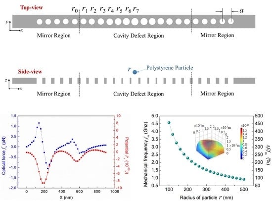
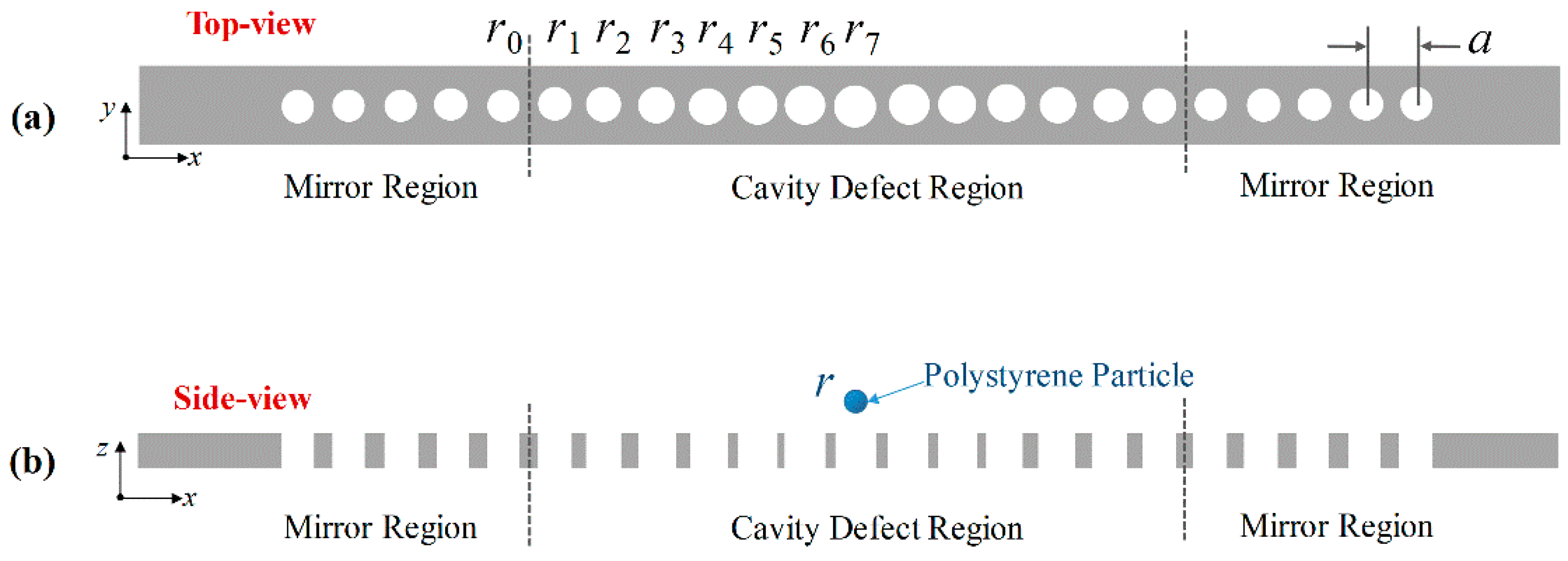
We designed a larger-center-hole nanobeam photonic crystal cavity fabricated on silicon-on-insulator for particle trapping and sensing. The structure of the cavity is shown in Figure 1a. The radius of air holes, rn, linearly increases from the mirror region to the center of the cavity defect region, where rn = r0 + 4 × n (nm). Here, r0 is fixed at a radius of 100 nm in the whole mirror region, and the largest hole in the center of the cavity defect region is set with a radius of r7 = 128 nm. For the entire structure, the lattice constant a, the distance between two adjacent holes, is kept as 365 nm. The width and the thickness of the nanobeam are 480 nm and 220 nm, respectively.
For particle trapping and sensing, the cavity was simulated in an aqueous environment with a polystyrene particle located above the center of the cavity, as shown in Figure 1b. The position of the polystyrene particle deviated from the center of the largest hole of the cavity in the x direction is denoted as Δx. The distance between the center of the polystyrene particle and the top surface of the nanobeam cavity in the z direction is denoted as Δz. The optical trapping force and the optical potential on the manipulated polystyrene particle were analyzed by varying its position based on the designed larger-center-hole nanobeam cavity. In the simulation, the material of the designed cavity and the particle are silicon and polystyrene, respectively, with the corresponding refractive index of 3.42 and 1.59. The whole cavity is set in aqueous environment, whose refractive index is 1.33. The Young’s modulus of the polystyrene is 3300 MPa.
The optical frequency of the defect mode in the photonic band structure of the designed cavity is presented in Figure 2a. The photonic band structure is calculated by plane wave expansion (PWE) method. It can be seen that the optical resonant mode is confined in the photonic band gap of the mirror structure. And the optical wavelength of the resonant cavity mode is calculated to be 1.5477 μm without the polystyrene particle. The optical transmission spectra of the designed cavity are simulated by finite-difference time-domain (FDTD) method and presented in Figure 2b. The optical quality factor (Q) of the cavity can be calculated from the transmission spectra and the Q factor for the designed cavity is 3968.
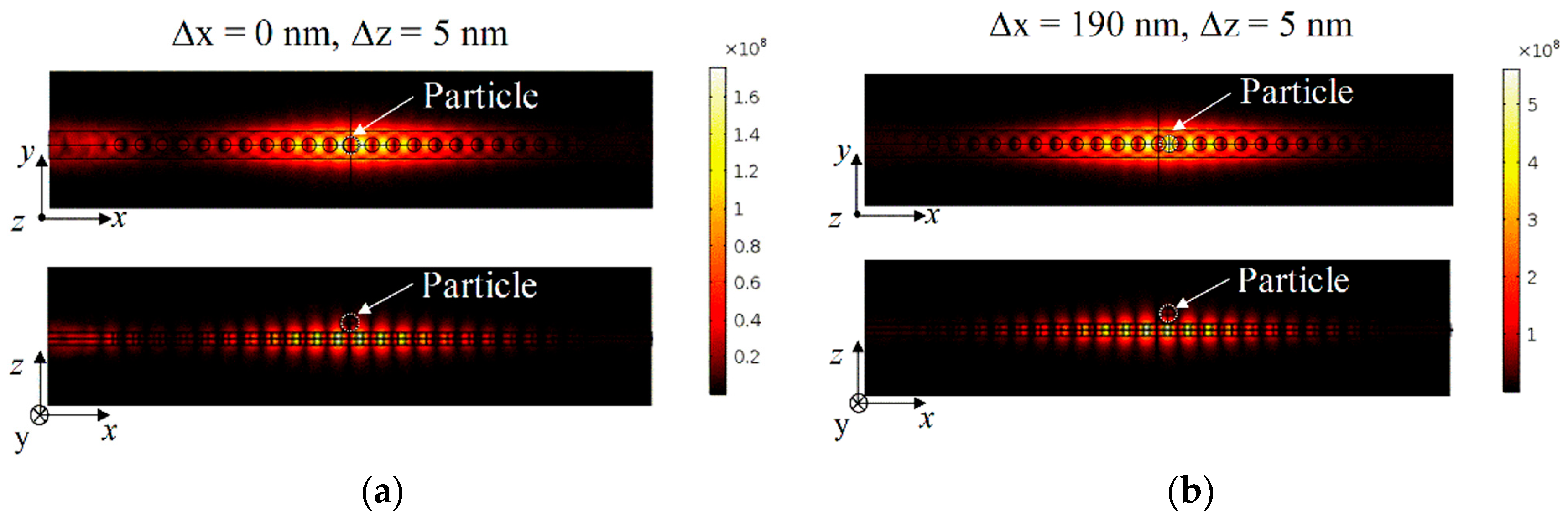
To study the optical trapping force and the optical potential on the polystyrene particle, the optical fields in x and z direction of the designed cavity with the polystyrene particle located at different positions were simulated and given in Figure 3. Here, the location of the polystyrene particle is set as (a) Δx = 0 nm, Δz = 5 nm and (b) Δx = 190 nm, Δz = 5 nm, respectively. It can be seen that the particle is located at the position of the largest optical field with Δx = 190 nm, Δz = 5 nm in Figure 3b. Accordingly a strong optical trapping can be achieved for the polystyrene particle at this position. This result can also be obtained by the calculation for the optical force and potential being applied on the polystyrene particle in the following, where a strong optical trapping potential for the polystyrene particle is located at Δx = 190 nm, Δz = 5.
2.2. Optical Force and Potential on a Particle
The optical force on the particle was calculated by the distribution of the electric field and magnetic field with Maxwell Stress Tensor [21]. In our calculation, the optical field of the designed cavity with the introduced polystyrene particle was first simulated by finite element analysis. Then, the optical force (f) on the particle was calculated by integrating the Maxwell stress tensor over the surfaces of the particle:
Where S is the surface of the particle, is the surface normal and T denotes the Maxwell stress tensor given as:
Where ε is the electric constant and μ0 is the magnetic constant, E is the electric field, B is the magnetic field, and δij is Kronecker’s delta function.
It should be noted that the potential is affected by the presence of the particle, since the refractive index of the polystyrene particle is larger than that of water. Thus, the optical force and potential were calculated with the particle located above the cavity. In the simulation, the light is input from one port of the nanobeam waveguide. Its frequency is set as the optical resonant frequency of the optical cavity with the particle located 5 nm above the cavity for the x direction (Δx is changed with Δz = 5). The calculated results are presented in Figure 4a. The calculation of optical force and potential on the particle in the z direction, in which the particle is located at a fixed Δx = 190 nm and a varied Δz, is shown in Figure 4b. Here, the negative and positive optical force refer to the direction of the force on the particle. For example, in the x direction, the negative or positive optical force refers to the force direction opposite or along the x axis, respectively. For the z direction, the negative optical forces indicate that the direction of the force is opposite the z axis, so that the particle will be trapped just above the cavity.
Since dielectric particles are attracted in the region of strongest electric field, a strong optical trapping can be realized in an optical cavity. When the light is input into the cavity, an optical potential in the x direction and the z direction around the cavity defect can be built for trapping the polystyrene particle with radius of 150 nm. For particle capturing, the minimum potential of 4.14 × 10⁻²⁰ J (10 kBT) is required at temperature of 300 K. For x direction, the potential well depth is 8.48 × 10⁻²⁰ J when the input power is 100 μW, as shown in Figure 4a. Since that the potential well depth increases linearly with the input light power, the input power is required to be 48.8 μW when the well depth reaches 4.14 × 10⁻²⁰ J (10 kBT). In addition, we also calculated the optical force and potential in the z direction while the particle is located at the strongest trapping of the potential well with Δx = 190 nm. As shown in Figure 4b, when the input power is 100 μW, the potential well depth is 9.17 × 10⁻²⁰ J. Thus, when the well depth reaches 10 kBT, the input power is required to be 45.1 μW. Taking the required input power for both x and z direction into consideration, it can be concluded that the input optical power is predicted as low as 48.8 μW for particles captured at 300 K. It should be mentioned that the coupling loss between the input light and the trapping cavity has been considered in our simulation. Thus, the input power for particle trapping using this proposed cavity is much lower compared with other reported work (120 μW–10 mW) [15,16], which benefits to mitigate the side effect on biological particles. In addition, it is possible to attract more than one particle from the water dispersion. It can be seen from Figure 4a that there is more than one potential well in the x direction. If the input optical power goes up, more potentials can be built for trapping multiple particles by the nanobeam photonic crystal cavity.
2.3. Optomechanical Sensing
Optomechanical coupling between cavity and particle inherently exists due to the mechanism of self-induced back-action optical trapping [16]. Based on optomechanical coupling, when we distinguish different particles, both the optical and mechanical frequency shift can be read out by the light output from the cavity. Here, the optical and mechanical frequency shift for the polystyrene particles with different radiuses ranging from 100 nm to 500 nm are calculated and shown in Figure 5a and 5b, respectively. The inset of Figure 5a shows the configuration for the detected nanobeam cavity with the particle located above the cavity.
When the particles with different radiuses, ranging from 100 nm to 500 nm, appear near the cavity, the surrounding refractive indices of the designed cavity change with a small variation, accordingly. Therefore, the optical resonant frequency of the cavity will shift dependent of the particles with different sizes. The changing percent of the optical resonant frequency of the cavity, Δf/fo, was also calculated and presented in Figure 5a. Here, the polystyrene particle is located at Δx = 190 nm, Δz = 5 nm. It can be seen that there is only a relative variation of ±0.06% approximatively for the optical frequency when the particle enlarged with radius from 100 nm to 500 nm.
On the other hand, the mechanical frequency of the particle decreases from 4.6 GHz to 0.9 GHz with the increasing size of the particles from 100 nm to 500 nm in radius. Here, the mechanical mode of the particle is the lowest order mechanical mode with the symmetric strain in the x, y, and z axes, which can be detected by the optomechanical coupling between the cavity and the particle due to the self-induced back-action optical trapping. The corresponding changing percent of the mechanical frequency of the cavity, Δf/fm, achieves approximately 400%. This is because the particle size significantly affects its mechanical frequency. Here, the strain for the vibrated particle with a radius of 200 nm is also given in the inset of Figure 5b. Therefore, compared with the optical frequency shift of ±0.06%, the mechanical frequency shift shows a better performance for particle sensing, which can be used to distinguish or analyze different particles with great potential.
3. Discussion
In this work, we calculated optical force and potential on an introduced polystyrene particle with radius of 150 nm generated by a larger-center-hole nanobeam photonic crystal cavity. The introduced polystyrene particle located over the cavity was simulated in an aqueous environment. For particles captured at a temperature of 300 K, the input optical power is required to be as low as 48.8 μW in the x direction and 45.1 μW in the z direction within the designed cavity. We also studied the sensing performance of the polystyrene particle dependent on different size by the resonant frequency shift of the optical cavity mode and mechanical mode. These results show a great potential of the designed nanobeam cavity for future lab-on-chip trapping and sensing applications.
Author Contributions
Conceptualization, L.R.; Data curation, L.R.; Formal analysis, L.R. and N.L.; Funding acquisition, Y.L.; Investigation, L.R., Y.L., N.L. and C.C.; Methodology, L.R. and Y.L.; Project administration, N.L.; Resources, C.C.; Software, L.R., Y.L. and N.L.; Supervision, N.L.; Validation, L.R., Y.L., N.L. and C.C.; Visualization, L.R.; Writing—original draft, L.R.; Writing—review & editing, L.R., Y.L., N.L. and C.C.
Funding
This research was funded by the National Natural Science Foundation of China (No. 61571462).
Acknowledgments
The authors would like to thank Chengzhi Yang for his invaluable discussion.
Conflicts of Interest
The authors declare no conflict of interest. The funders had no role in the design of the study; in the collection, analyses, or interpretation of data; in the writing of the manuscript, or in the decision to publish the results.
References
- Van Thourhout, D.; Roels, J. Optomechanical Device Actuation through the Optical Gradient Force. Nat. Photonics 2010, 4, 211–217. [Google Scholar] [CrossRef]
- Van Leest, T.; Caro, J. Cavity-Enhanced Optical Trapping of Bacteria Using a Silicon Photonic Crystal. Lab. Chip 2013, 13, 4358–4365. [Google Scholar] [CrossRef] [PubMed]
- Quan, Q.; Floyd, D.L.; Burgess, I.B.; Deotare, P.B.; Frank, I.W.; Tang, S.K.Y.; Ilic, R.; Loncar, M. Single Particle Detection in CMOS Compatible Photonic Crystal Nanobeam Cavities. Opt. Express 2013, 21, 32225–32233. [Google Scholar] [CrossRef] [PubMed]
- Renaut, C.; Cluzel, B.; Dellinger, J.; Lalouat, L.; Picard, E.; Peyrade, D.; Hadji, E.; de Fornel, F. On Chip Shapeable Optical Tweezers. Sci. Rep.-UK 2013, 3, 2290. [Google Scholar] [CrossRef] [PubMed]
- Akahane, Y.; Asano, T.; Song, B.S.; Noda, S. High-Q Photonic Nanocavity in a Two-Dimensional Photonic Crystal. Nature 2003, 425, 944–947. [Google Scholar] [CrossRef]
- Zhao, Q.; Cui, K.; Feng, X.; Liu, F.; Zhang, W.; Huang, Y. Low Loss Sharp Photonic Crystal Waveguide Bends. Opt. Commun. 2015, 355, 209–212. [Google Scholar] [CrossRef]
- Zhao, Q.; Cui, K.; Huang, Z.; Feng, X.; Zhang, D.; Liu, F.; Zhang, W.; Huang, Y. Compact Thermo-Optic Switch Based on Tapered W1 Photonic Crystal Waveguide. IEEE Photonics J. 2013, 5. [Google Scholar] [CrossRef]
- Zhao, Q.; Cui, K.; Feng, X.; Liu, F.; Zhang, W.; Huang, Y. Variable Optical Attenuator Based on Photonic Crystal Waveguide with Low-Group-Index Tapers. Appl. Opt. 2013, 52, 6245–6249. [Google Scholar] [CrossRef]
- Deotare, P.B.; McCutcheon, M.W.; Frank, I.W.; Khan, M.; Loncar, M. High Quality Factor Photonic Crystal Nanobeam Cavities. Appl. Phys. Lett. 2009, 94, 121106. [Google Scholar] [CrossRef]
- Quan, Q.; Deotare, P.B.; Loncar, M. Photonic Crystal Nanobeam Cavity Strongly Coupled to the Feeding Waveguide. Appl. Phys. Lett. 2010, 96, 203102. [Google Scholar] [CrossRef]
- Quan, Q.; Loncar, M. Deterministic Design of Wavelength Scale, Ultra-High Q Photonic Crystal Nanobeam Cavities. Opt. Express 2011, 19, 18529–18542. [Google Scholar] [CrossRef] [PubMed]
- Seidler, P.; Lister, K.; Drechsler, U.; Hofrichter, J.; Stoeferle, T. Slotted Photonic Crystal Nanobeam Cavity with an Ultrahigh Quality Factor-To-Mode Volume Ratio. Opt. Express 2013, 21, 32468–32483. [Google Scholar] [CrossRef] [PubMed]
- Han, S.; Shi, Y. Systematic Analysis of Optical Gradient Force in Photonic Crystal Nanobeam Cavities. Opt. Express 2016, 24, 452–458. [Google Scholar] [CrossRef]
- Chen, Y.; Serey, X.; Sarkar, R.; Chen, P.; Erickson, D. Controlled Photonic Manipulation of Proteins and Other Nanomaterials. Nano Lett. 2012, 12, 1633–1637. [Google Scholar] [CrossRef] [Green Version]
- Serey, X.; Mandal, S.; Erickson, D. Comparison of Silicon Photonic Crystal Resonator Designs for Optical Trapping of Nanomaterials. Nanotechnology 2010, 21, 305202. [Google Scholar] [CrossRef] [PubMed]
- Descharmes, N.; Dharanipathy, U.P.; Diao, Z.; Tonin, M.; Houdre, R. Observation of Backaction and Self-Induced Trapping in a Planar Hollow Photonic Crystal Cavity. Phys. Rev. Lett. 2013, 110, 123601. [Google Scholar] [CrossRef]
- Huang, Z.; Cui, K.; Li, Y.; Feng, X.; Liu, F.; Zhang, W.; Huang, Y. Strong Optomechanical Coupling in Nanobeam Cavities Based on Hetero Optomechanical Crystals. Sci. Rep.-UK 2015, 5, 15964. [Google Scholar] [CrossRef]
- Pan, F.; Cui, K.; Bai, G.; Feng, X.; Liu, F.; Zhang, W.; Huang, Y. Radiation-Pressure-Antidamping Enhanced Optomechanical Spring Sensing. ACS Photonics 2018, 5, 4164–4169. [Google Scholar] [CrossRef]
- Li, Y.; Cui, K.; Feng, X.; Huang, Y.; Huang, Z.; Liu, F.; Zhang, W. Optomechanical Crystal Nanobeam Cavity with High Optomechanical Coupling Rate. J. Opt.-UK 2015, 17, 045001. [Google Scholar] [CrossRef]
- Huang, Z.; Cui, K.; Bai, G.; Feng, X.; Liu, F.; Zhang, W.; Huang, Y. High-Mechanical-Frequency Characteristics of Optomechanical Crystal Cavity with Coupling Waveguide. Sci. Rep.-UK 2016, 6, 34160. [Google Scholar] [CrossRef]
- Barton, J.P.; Alexander, D.R.; Schaub, S.A. Theoretical Determination of Net-Radiation Force and Torque for a Spherical-Particle Illuminated by a Focused Laser-Beam. J. Appl. Phys. 1989, 66, 4594–4602. [Google Scholar] [CrossRef]
Figure 1.
(a) Top-view and (b) Side-view of the structure of the larger-center-hole nanobeam photonic crystal cavity, above which a polystyrene particle is introduced. The position of the polystyrene particle deviates from the center of the largest hole of the cavity in the x direction is denoted as Δx. The distance between the center of the polystyrene particle and the top surface of the nanobeam cavity in the z direction is denoted as Δz.

Figure 2.
(a) The photonic band structure of the larger-center-hole nanobeam photonic crystal cavity. The optical frequency of the defect mode of the designed cavity is also presented in the photonic band gap with dash line. (b) The optical transmission spectra of the designed cavity calculated by finite-difference time-domain (FDTD) simulation with resonant wavelength of 1.5477 μm and Q factor of 3968.

Figure 3.
The optical fields in x and z direction of the designed cavity with polystyrene particle located at different position (a) Δx = 0 nm, Δz = 5 nm, and (b) Δx = 190 nm, Δz = 5 nm.
Figure 3.
The optical fields in x and z direction of the designed cavity with polystyrene particle located at different position (a) Δx = 0 nm, Δz = 5 nm, and (b) Δx = 190 nm, Δz = 5 nm.

Figure 4.
The optical force and potential on the particle (a) in the x direction and (b) in the z direction with the input light power of 100 μW.
Figure 4.
The optical force and potential on the particle (a) in the x direction and (b) in the z direction with the input light power of 100 μW.
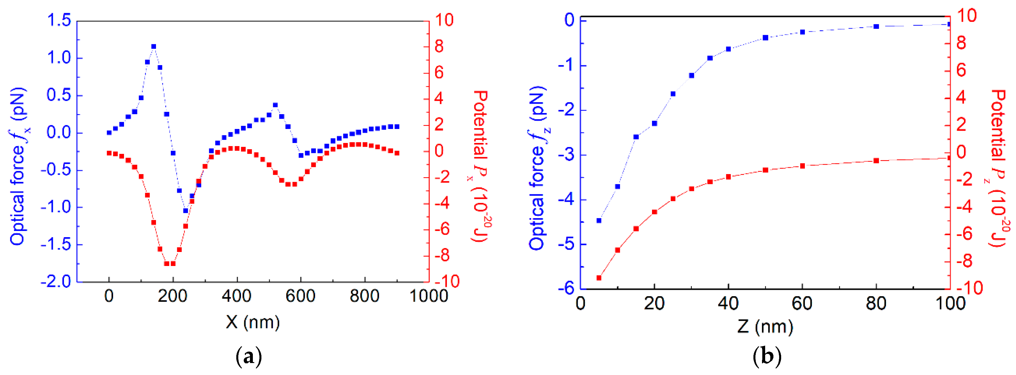
Figure 5.
(a) The optical frequency shift for the particle with different radius, ranging from 100 nm to 500 nm. The relative changing percent of the optical resonant frequency of the cavity, Δf/fo, was also calculated. Here, the polystyrene particle is located at Δx = 190 nm, Δz = 5 nm. The inset shows the configuration for the detected nanobeam cavity with the particle above the cavity. (b) The mechanical frequency shift and the relative changing percent of the mechanical frequency of the cavity, Δf/fm for the particle with a different radius. The inset shows the strain for the vibrated particle with a radius of 200 nm.

© 2019 by the authors. Licensee MDPI, Basel, Switzerland. This article is an open access article distributed under the terms and conditions of the Creative Commons Attribution (CC BY) license (http://creativecommons.org/licenses/by/4.0/).
Share and Cite
MDPI and ACS Style
Ren, L.; Li, Y.; Li, N.; Chen, C. Trapping and Optomechanical Sensing of Particles with a Nanobeam Photonic Crystal Cavity. Crystals 2019, 9, 57. https://doi.org/10.3390/cryst9020057
AMA Style
Ren L, Li Y, Li N, Chen C. Trapping and Optomechanical Sensing of Particles with a Nanobeam Photonic Crystal Cavity. Crystals. 2019; 9(2):57. https://doi.org/10.3390/cryst9020057
Chicago/Turabian StyleRen, Lin, Yunpeng Li, Na Li, and Chao Chen. 2019. "Trapping and Optomechanical Sensing of Particles with a Nanobeam Photonic Crystal Cavity" Crystals 9, no. 2: 57. https://doi.org/10.3390/cryst9020057
Note that from the first issue of 2016, this journal uses article numbers instead of page numbers. See further details here.