1. Introduction
GaAs is a semiconductor compound used in some diodes, field-effect transistors (FETs), and integrated circuits (ICs). It has high carrier mobility, a high optical absorption coefficient and a direct bandgap energy of E
g = 1.42 eV [
1]. This makes GaAs components useful at ultra-high radio frequencies and in fast electronic switching applications. GaAs devices generate less noise than most other types of semiconductor components.
Due to the technological interest in GaAs, different techniques have been developed to obtain this semiconductor. GaAs single crystals can be prepared by industrial processes such as the Czochralski method, the vertical gradient freeze process or the Bridgman-Stockbarger technique [
2,
3]. Alternative methods to obtain GaAs films include [
3,
4], vapor-phase epitaxy [
5], metalorganic chemical vapor deposition (MOCVD) [
4], and molecular beam epitaxy [
6]. Another variation of film deposition technique derived from chemical vapor deposition (CVD) is the close-spaced vapor transport (CSVT) method [
7,
8,
9].
The CSVT method has been successfully used to grow a variety of thin films semiconductor materials, including homo-and hetero-epitaxial GaAs films [
7]. This technique has some advantages compared to the other ones. It is a low-cost manufacturing technique that allows the deposition of thin films at atmospheric pressure and moderates temperatures [
8,
9]. The main difference with the other techniques is that in the CSVT, the source of the material to be deposited as a thin film on the substrate is the material itself. This allows multiple deposits with one single or polycrystalline source materials. The source and the substrate are located in the reactor and separated by a thin spacer.
In this method the task of the transport agent is to make contact with the source to produce volatile compounds [
10], which are subsequently transported by the temperature gradient between the source-substrate and deposited on the surface of the substrate [
11] (quartz, sapphire, silicon, graphite, etc.). Also, CSVT is a typical technique used for GaAs growth [
12,
13]. The use of this technique for the case of GaAs started with water vapor as a transport agent; creating volatile compounds as GaO
2 and As
2 [
14]. The problem was that due to the incorporation of oxygen in the GaAs layer growth, the electronic mobility is negatively affected [
2,
15]. To avoid this effect, atomic hydrogen has been used as the transport agent to create volatile compounds [
12,
13,
16]. These volatile compounds favor the material transport in a CSVT system. The gaseous atmosphere used in the process has an important role in the properties and characteristics of the produced films [
17].
The aim of this work is to observe the effect in the crystalline quality, surface morphology and growth rate using hydrogen and nitrogen as gaseous atmospheres by the CSVT technique. Scanning electron microscopy (SEM), energy dispersive spectroscopy (EDS), micro-Raman spectroscopy, UV-VIS spectroscopy and X-ray diffraction (XRD) were the techniques used in this study.
2. Experimental Details
Figure 1 shows the scheme of the CSVT setup used in this work. The GaAs solid source was heated with a tungsten incandescent filament (OSRAM-P28S, OSRAM, Munich, Germany) and kept at 2000 °C inside a hermetic home-made reactor. As a substrate, a quartz piece of 2 × 2 cm was used; as a separator, a quartz o-ring of 10 mm in diameter and 2 mm in height. As the solid source a GaAs (111) wafer with a resistivity of 10 Ω·cm was used. The gaseous atmospheres used were hydrogen and nitrogen of chromatographic grade supplied by INFRA. Two growth processes were carried out, one in a hydrogen atmosphere and the other in a nitrogen atmosphere; both were at atmospheric pressure. The flow of molecular gas passes through the hot filament cracking some of the molecular species; subsequently, it travels towards the source of GaAs to create volatile compounds. The hot filament also simultaneously heats the substrate and the source maintaining a temperature gradient between them, which facilitates the transport of material. The following reactions were proposed for the two different gaseous atmospheres:
Chemical reactions proposed in the H
2 atmosphere:
Chemical reactions proposed in the N
2 atmosphere:
In this experiment the reactor was closed and purged three times before the introduction of the carrier gas (N2 or H2) with a flow rate of 110 cm3·min−1. The filament was heated to reach a temperature of 2000 °C. The space between the filament and the GaAs source was calibrated to obtain a temperature approximated at 830 °C. Two different deposition times were established, which were 5 and 13 min. The morphological and chemical characterization was performed using a scanning electron microscope (SEM), model JEOL JSM 7401F (JEOL, Tokyo, Japan). UV-Vis measurements were taken in a Cary 5000 spectrophotometer (Agilent, Santa Clara, CA, USA). Films thickness were measured with a Dektak 150 profilometer (Veeco, New York, NY, USA). Raman spectra were obtained with a Micro-Raman Horiba LabRAM-HR spectrometer (Horiba, Kyoto, Japan) and the structural characterization was carried out with a BRUKER AXS D8 Discovery diffractometer (Bruker, Billerica, MA, USA). A copper radiation with a wavelength of 1.54 Å was used.
3. Results and Discussion
3.1. Surface Morphology
Surface morphology of the GaAs films growth by CSVT technique using H
2 and N
2 as gaseous atmospheres on a quartz substrate is shown in
Figure 2. The magnification of the four images is ×2000. The layers grown in hydrogen atmosphere correspond to
Figure 2a,b with time of 5 min and 13 min, respectively. The atmosphere of H
2 produces a homogeneous and almost continuous layer (some cracks were detected over the entire sample, the cracks are due to the strains that the film is subjected to) and a relatively continuous surface was observed. When the deposition time was enlarged at 13 min, the GaAs layer thickness increased and less cracks were observed on the surface.
For the case of the layers grown in nitrogen atmosphere a granular morphology is observed; (c) and (d) with 5 and 13 min of deposition time, respectively. Different cluster sizes are presented in (c) and exhibited rough grains in the micron scale range, while in (d) similar cluster sizes are observed along with a uniform increase of the thickness and less roughness of the grains.
3.2. Band Gap
Figure 3a shows the UV–VIS transmittance spectra of GaAs films deposited on quartz. The samples grown using hydrogen as gaseous atmosphere exhibit the highest and lowest transmittance. The sample of 5 min (blue solid line) exhibit a transmittance higher than 40% between 1000 and 2000 nm; while the layer grown to 13 min (red solid line) shows a low transmittance compared to the previous sample. Having a longer deposition time enhances the amount of volatile compounds that help the transport of material and therefore the thickness of the film increases. For the samples grown using the nitrogen atmosphere, a similar behavior is shown for the two deposition times (black and orange solid line). The two films have a transmittance between 10 and 20 percent. With the assistance of a profilometer it is observed that the growth of the film is slower with nitrogen, see
Table 1. In comparison with hydrogen, nitrogen is less reactive [
18], causing fewer volatile compounds when reacting with the source.
The approximate values of the energy band gap (E
g) were obtained by the relationship known as Tauc plot [
19,
20] as shown in
Figure 3b. The methodology for obtaining these approximate values of E
g has been described in reference [
21]; where the absorption coefficients α (λ) were determined from transmission spectra. For hydrogen atmosphere samples we have 1.861 and 1.663 eV; while 1.774 and 1.644 for nitrogen atmosphere. The growth time was 5 and 13 min, respectively.
In spite of the efforts to control film growth; GaAs material contains a number of crystal defects, dislocations and impurities [
22]. This causes the value of E
g in both atmospheres and the times to increase with respect to the bulk value of GaAs, see
Table 1. In addition, the bandgap decreases as the thickness increases [
23]. Although the results of EDS and XRD (which are presented below) show that there is a greater number of defects in the samples grown in the nitrogen atmosphere, E
g turns out to be higher in the films deposited in a hydrogen atmosphere. However, it has been reported that the introduction of a small amount of nitrogen within the GaAs lattice may decrease E
g values [
24,
25]. Therefore, we believe that the incorporation of nitrogen has a greater influence, causing that Eg to be smaller in the films deposited in the nitrogen atmosphere. Also as demonstrated above the presence of N
2 in the deposition of GaAs stimulates the formation of a granular surface. This behavior has been previously observed in the CVD process for the growth of diamond films, where they exhibited a substantial change in the film morphology and grain size in absence or presence of N
2 [
17,
26].
3.3. Energy Dispersive Spectroscopy (EDS) Analysis
EDS spectrum has been determined from different regions of the GaAs films, see
Table 2. According to the analysis of the results, for GaAs layers grown in a hydrogen atmosphere the amount of Ga is very close to the As. (on average 52 at% and 48 at%, respectively). There is no trace of oxygen. Meanwhile in the samples obtained under nitrogen atmosphere a film rich in Ga (on average 45 at% of Ga and 36 at% of As) is obtained, but with the presence of O (on average 15 at%) and N (on average 2.5 at%); meaning, more impurities and defects in the films of GaAs. We believe that the impurities come from the gas source. The non-stoichiometry of the GaAs over layers is due to the nature of the CSVT growth process, since it is known that the GaAs dissociates with preferential evaporation of arsenic at high temperature, and that the species leaving GaAs at evaporation are Ga and As
2 [
27].
3.4. Crystalline Structure
Figure 4 shows the X-ray diffraction spectra of the GaAs films obtained by CSVT technique. The diffractometer was set to select the CuK
α1 wavelength. GaAs zinc-blende crystalline structure is recognized by three major diffraction peaks at 27.29° 45.36° and 53.70°. The full width at half-maximum (FWHM) [
28] values of the samples were determined with the following equation:
FWHMsample is the broad at the average height of the diffraction peak of the sample, D is the deconvolution parameter, it changes according to the profile type of the diffraction peak, for a Gaussian profile D = 2 and for a Lorentzian profile D = 1. FWHMmeasure is the broad at the average height of the diffraction peak measured on the diffractometer. FWHMinstrumental is the contribution of the broad to the average height derivative by the instrument and is calculated by the instrumental function of the X-ray equipment.
The measure and the instrumental broadening were determined by fitting the peak to a Gaussian function and, the crystallite size using the Scherrer’s equation, see
Table 3. To calculate the crystallite size, a diffraction peak was chosen that is approximately two theta equal to 27°. The
FWHMsample value is converted to radians to be replaced in the Scherrer’s equation and the crystallite size takes the units of the wavelength.
In the samples (5 and 13 min) using hydrogen as gaseous atmosphere, it is observed that the three peaks corresponding to the directions (111), (220) and (311) with a strong crystalline domain of the direction (111) present much greater diffraction than the other two directions. It is observed that the peak is tighter in the sample of 13 min due to the fact that while the deposition time is longer there will be a better rearrangement of the atoms. This results in a better crystallinity degree that leads to a larger crystallite size. While the FWHMsample obtained for the 5 min sample is 0.055° with an approximate crystallite size of 147 nm, for the film obtained with a deposition time of 13 min we have a lower FWHMsample, 0.015, but a larger crystallite size of approximately 543 nm.
The diffraction pattern of the samples grown in the nitrogen atmosphere also show a preference for the direction (111) but without becoming as dominant as in the samples obtained in the hydrogen atmosphere. This coexistence of the three directions generates a tension between the borders of the crystalline domains, which causes a displacement of the peaks. In the case of the peak in the direction (111), a small shift to the left is observed.
The broadening is probably due to impurities, as shown in the EDS results and the crystallite size being lower in these films obtained in nitrogen atmosphere. These crystallites of approximately 24 nm (5 min) and 67 nm (13 min) directly affect the crystallinity degree, being 0.329° and 0.121°, respectively. We think that due to defects, impurities and microstrains, no photoluminescence was observed.
3.5. Micro-Raman Analysis
Literature reports that for a zinc-blende structure as the GaAs, the vibrational modes TO and LO depend on the crystal orientation and the dispersion geometry [
29]. If the geometry used is back scattering; the orientation (001) of the crystal only the LO mode is allowed, while the TO mode is prohibited. In the orientation (110) only the TO mode appears while both TO and LO phonons contribution appear in the direction (111). According to these statements and with the results obtained from X-rays, it is evident that we would obtain the TO phonon and the LO phonon given the preferential orientation (111) for the samples grown in hydrogen atmosphere as in nitrogen atmosphere.
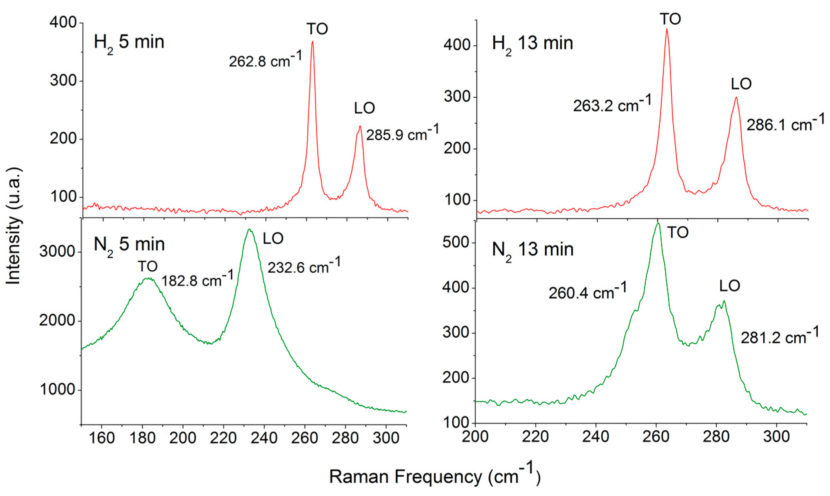
Figure 5 shows typical Raman spectra, recorded at room temperature under non-resonant conditions. The measurements were made with a Horiba-Jobin Yvon spectrometer, model LabRam-HR with a He-Ne laser at 632.8 nm. The light was focused to a diameter of 6 mm at the sample using ×50. The power laser used in these measurements was 0.5 mW. For those samples of GaAs grown in hydrogen atmosphere (represented by a red continuous line) the spectrum is dominated by two prominent features located around 263 and 286 cm
−1. These modes show appreciable shifts in comparison with the GaAs bulk frequencies (269 and 292 cm
−1 for the TO and the LO, respectively [
30,
31]), so the post-growth tensile stress can be considered for this samples.
The calculated FWHM of the films grown (5 and 13 min) in a hydrogen atmosphere is very close and does not help to conclude which of these presents a better crystallinity. The shift of the peak is also very close. In the case of the samples grown in a nitrogen atmosphere (represented by a continuous green line), a greater shift and a broadening of the peaks are observed. This is not only attributed to the post-growth tensile stress, but also to the introduced impurities (nitrogen and oxygen) as shown by the EDS results. These impurities increase the existing mismatch of the lattice constants between substrate-film [
32].
For the 13-min sample, the TO mode is around 260 cm
−1 and the LO mode is approximately 281 cm
−1, a significant shift. The peak observed at 260 cm
−1 presents a shoulder feature attributed to As-As vibration [
33]. Something interesting is observed in the sample that was obtained with a deposition time of 5 min, which is that the shift is very large. We infer that this behavior is due to the fact that during the first minutes macrostrains are created and the mismatch of the lattice constants turns out to be disproportionate. Remember that with N
2 a smaller amount of volatile compounds is generated and consequently a slow deposition is obtained. As time passes, a reordering takes place in situ. It can be noticed in the evolution of the spectrum of the sample of 5 min to that of 13 min. This can be corroborated with the results of EDS, where it is observed that the amount of impurities (nitrogen and oxygen) decreases with an increasing time. In addition, in X-rays the peak corresponding to the direction (111) is wider in the sample of 5 min.
4. Conclusions
Layers of GaAs were deposited using gaseous atmosphere of nitrogen and hydrogen by the CSVT technique. The effect of using different atmospheres resulted in GaAs films with different characteristics. In the SEM micrographs a continuous surface was observed in a hydrogen atmosphere than in nitrogen, where the surface is completely granular. The transmittance results show that larger the thickness, higher the transmittance. In addition, the value of Eg increased with respect to the value in bulk of the GaAs in both atmospheres, being greater in the hydrogen atmosphere. The EDS results showed the incorporation of oxygen and nitrogen in the case of the nitrogen atmosphere. The diffraction patterns obtained by XRD showed that in a nitrogen atmosphere, the peaks turned out to be broader and have a small displacement towards the left. In the same way the Raman spectra showed that the impurities introduced had a considerable impact, this was observed in the displacements and broadening of the peaks in the films obtained in the nitrogen atmosphere. This work obtained by the CSVT technique, shows the possibility to obtain many layers of GaAs better quality in a hydrogen atmosphere, from a single source provided by a GaAs wafer, that implies a lower cost for the device manufacturing.
Author Contributions
J.J.C.B., G.G.S. and R.F.B.V., wrote, conceived and designed the experiments; J.A.L.L., F.G.N.C., T.D.B. and E.R.A. provided resources and systems; A.C.S., R.R.T., C.M.R., R.G.I. and J.M.G.J. provided support in review and editing this work.
Acknowledgments
This work was supported by “Vicerrectoría de Investigación y Estudios de Posgrado, (100065344-VIEP2018)” and “Programa para el Desarrollo Profesional Docente (DSA/103.5/16/7345)”. The authors acknowledge ICUAP and IFUAP laboratories for their help in the sample measurements.
Conflicts of Interest
The authors declare no conflict of interest. The funders had no role in the design of the study; in the collection, analyses, or interpretation of data; in the writing of the manuscript, or in the decision to publish the results.
References
- Adachi, S. Physical Properties of III-V Semiconductor Compounds; Wiley: Hoboken, NJ, USA, 1992. [Google Scholar]
- Moss, S.J.; Ledwith, A. The Chemistry of the Semiconductor Industry; Blackie: Houston, TX, USA, 1987. [Google Scholar]
- Scheel, H.J.; Fukuda, T. Crystal Growth Technology; Wiley: Hoboken, NJ, USA, 2003. [Google Scholar]
- Smart, L.; Elaine, E.; Moore, A. Solid State Chemistry: An Introduction; CRC Press: Boca Raton, FL, USA, 2012. [Google Scholar]
- Stringfellow, G.B. Organometallic Vapor-Phase Epitaxy: Theory and Practice; Academic Press: Cambridge, MA, USA, 1999. [Google Scholar]
- Cho, A.Y.; Arthur, J.R. Molecular beam epitaxy. Prog. Solid State Chem. 1975, 10, 157–191. [Google Scholar] [CrossRef]
- Gottlieb, G.E.; Corboy, J.F. Epitaxial growth og GaAs using water vapor. RCA Rev. 1963, 24, 585–595. [Google Scholar]
- Massé, G.; Lacroix, J.M.; Lawrence, M.F. Deep-level transient spectroscopy study of n-type GaAs epitaxial layers grown by close-spaced vapor transport. J. Appl. Phys. 1989, 65, 1126–1129. [Google Scholar] [CrossRef]
- Sagna, A.; Djessas, K.; Sene, C.; Medjnoun, K.; Grillo, S.E. Close spaced vapor transport deposition of Cu2ZnSnS4 thin films: Effect of iodine pressure. J. Alloys Compd. 2016, 685, 699–704. [Google Scholar] [CrossRef]
- Gómez-Barojas, E.; Silva-González, R.; Gracia-Jiménez, J.M.; Navarro-Contreras, H.; Vidal-Borbolla, M.A. Characterization of GaAs grown by the close-spaced vapor transport technique, using atomic hydrogen as the reactant. Phys. Status Solidi 2003, 198, 289–296. [Google Scholar] [CrossRef]
- Park, J.-H.; Sudarshan, T.S. Chemical Vapor Deposition; ASM International: Geauga County, OH, USA, 2001. [Google Scholar]
- Ritenour, A.J.; Boucher, J.W.; DeLancey, R.; Greenaway, A.L.; Aloni, S.; Boettcher, S.W. Doping and electronic properties of GaAs grown by close-spaced vapor transport from powder sources for scalable III–V photovoltaics. Energy Environ. Sci. 2015, 8, 278–285. [Google Scholar] [CrossRef]
- Silva-Andrade, F.; Ilinskii, A.; Chavez, F.; Prutskij, T.; Tenorio, F.; Bravo-Garcia, Y.; Pena-Sierra, R. Growth and Characterization of GaAs p-n Junctions Obtained by the CSVT Technique using Atomic Hydrogen. Mod. Phys. Lett. B 2001, 15, 752–755. [Google Scholar] [CrossRef]
- Hammadi, M.; Bourgoin, J.C.; Samic, H. Mechanism of GaAs transport by water reaction application to the growth of thick epitaxial layers. J. Mater. Sci. Mater. Electron. 1999, 10, 399–402. [Google Scholar] [CrossRef]
- Sun, G.C.; Zazoui, M.; Talbi, N.; Khirouni, K.; Bourgoin, J.C. Mobility-lifetime product in epitaxial GaAs X-ray detectors. Nucl. Instrum. Methods Phys. Res. Sect. A Accel. Spectrom. Detect. Assoc. Equip. 2007, 573, 228–231. [Google Scholar] [CrossRef]
- Kobayashi, R.; Fujii, K.; Hasegawa, F. Etching of GaAs by Atomic Hydrogen Generated by a Tungsten Filament. Jpn. J. Appl. Phys. 1991, 30, L1447–L1449. [Google Scholar] [CrossRef]
- Jung, M.; Eun, K.Y.; Lee, J.-K.; Baik, Y.-J.; Lee, K.-R.; Park, J.W. Growth of carbon nanotubes by chemical vapor deposition. Diam. Relat. Mater. 2001, 10, 1235–1240. [Google Scholar] [CrossRef]
- Parry, R.W.; Bassow, H.; Merrill, P. Chemistry, Experimental Foundations; Prentice-Hall: Upper Saddle River, NJ, USA, 1987. [Google Scholar]
- Wang, L.; Han, K.; Tao, M. Effect of Substrate Etching on Electrical Properties of Electrochemically Deposited CuO. J. Electrochem. Soc. 2007, 154, D91. [Google Scholar] [CrossRef]
- Pankove, J.I. Optical Processes in Semiconductors; Prentice Hall: Englewood Cliffs, NJ, USA, 1971. [Google Scholar]
- López, J.A.; López, J.C.; Valerdi, D.V.; Salgado, G.G.; Díaz-Becerril, T.; Pedraza, A.P.; Gracia, F.F. Morphological, compositional, structural, and optical properties of Si-nc embedded in SiOx films. Nanoscale Res. Lett. 2012, 7, 604. [Google Scholar] [CrossRef] [PubMed]
- Kayali, S.; Ponchak, G.; Shaw, R. GaAs MMIC Reliability Assurance Guideline forSpace Applications Preface. JPL Publ. 1996, 96, 58. [Google Scholar]
- Das, C.; Begum, J.; Begum, T.; Choudhury, S. Effect of thickness on the optical properties of Gaas thin films. J. Bangladesh Acad. Sci. 2013, 37, 83–91. [Google Scholar] [CrossRef] [Green Version]
- Cheong, H.M.; Zhang, Y.; Mascarenhas, A.; Geisz, J.F. Nitrogen-induced levels in GaAs 1 − x N x studied with resonant Raman scattering. Phys. Rev. B 2000, 61, 13687–13690. [Google Scholar] [CrossRef]
- Wei, S.-H.; Zunger, A. Giant and Composition-Dependent Optical Bowing Coefficient in GaAsN Alloys. Phys. Rev. Lett. 1996, 76, 664–667. [Google Scholar] [CrossRef] [PubMed]
- Bohr, S.; Haubner, R.; Lux, B. Influence of nitrogen additions on hot-filament chemical vapor deposition of diamond. Appl. Phys. Lett. 1996, 68, 1075–1077. [Google Scholar] [CrossRef]
- Foxon, C.T.; Harvey, J.A.; Joyce, B.A. The evaporation of GaAs under equilibrium and non-equilibrium conditions using a modulated beam technique. J. Phys. Chem. Solids 1973, 34, 1693–1701. [Google Scholar] [CrossRef]
- Vashista, M.; Paul, S. Correlation between full width at half maximum (FWHM) of XRD peak with residual stress on ground surfaces. Philos. Mag. 2012, 92, 4194–4204. [Google Scholar] [CrossRef]
- Pollak, F.H. Semiconductor Characterization by Raman Spectroscopy; Test and Measurements World: San Francisco, CA, USA, 1985. [Google Scholar]
- Tiong, K.K.; Amirtharaj, P.M.; Pollak, F.H.; Aspnes, D.E. Effects of As+ ion implantation on the Raman spectra of GaAs: ‘“Spatial correlation”’ interpretation. Appl. Phys. Lett. 1984, 44, 122–124. [Google Scholar] [CrossRef]
- Iikawa, F.; Cerdeira, F.; Vazquez-Lopez, C.; Motisuke, P.; Sacilotti, M.A.; Roth, A.P.; Masut, R.A. Raman Scattering from InGaAs/GaAs strained-layer superlattices. Solid State Commun. 1988, 68, 211–214. [Google Scholar] [CrossRef]
- Jain, S.C.; Willander, M.; Maes, H. Stresses and strains in epilayers, stripes and quantum structures of III-V compound semiconductors. Semicond. Sci. Technol. 1996, 11, 641–671. [Google Scholar] [CrossRef]
- Lannin, J.S.; Calleja, J.M.; Cardona, M. Second-order Raman scattering in the group-V semimetals: Bi, Sb, and As. Phys. Rev. B 1975, 12, 585–593. [Google Scholar] [CrossRef]
© 2019 by the authors. Licensee MDPI, Basel, Switzerland. This article is an open access article distributed under the terms and conditions of the Creative Commons Attribution (CC BY) license (http://creativecommons.org/licenses/by/4.0/).

 ,
, 


