Growth of Multi-Layer hBN on Ni(111) Substrates via MOCVD
by
Gene Siegel
1,2, 
Gordon Gryzbowcki
1,2,
Albert Hilton
2,3,
Christopher Muratore
4 and
Michael Snure
1,* 1
Air Force Research Laboratory, Sensor Directorate, 2241 Avionics Circle, Wright Patterson AFB, OH 45433, USA
2
KBR, 2241 Avionics Circle, Wright Patterson AFB, OH 45433, USA
3
Air Force Research Laboratory, Materials and Manufacturing Directorate, 2941 Hobson Way, Wright Patterson AFB, OH 45433, USA
4
University of Dayton, Department of Chemical and Materials Engineering, 300 College Park, Dayton, OH 45469, USA
*
Author to whom correspondence should be addressed.
Crystals 2019, 9(7), 339; https://doi.org/10.3390/cryst9070339
Submission received: 5 June 2019
/
Revised: 24 June 2019
/
Accepted: 29 June 2019
/
Published: 2 July 2019
(This article belongs to the Special Issue Inorganic Layered Crystals: From Fundamentals to Materials Performance)
Abstract
:In this paper we demonstrate a metal organic chemical vapor deposition (MOCVD) process for growth of few layer hBN films on Ni(111) on sapphire substrates using triethylborane (TEB) and ammonia (NH3). Ni(111) was selected as a substrate due to its symmetry and close lattice matching to hBN. Using atomic force microscopy (AFM) we find hBN is well aligned to the Ni below with in plane alignment between the hBN zig zag edge and the <110> of Ni. We further investigate the growth process exploring interaction between precursors and the Ni(111) substrate. Under TEB pre-exposure Ni-B and graphitic compounds form which disrupts the formation of layered phase pure hBN; while NH3 pre-exposure results in high quality films. Tunnel transport of films was investigated by conductive-probe AFM demonstrating films to be highly resistive. These findings improve our understanding of the chemistry and mechanisms involved in hBN growth on metal surfaces by MOCVD.
1. Introduction
In the past several years, much research has been done into the field of two-dimensional (2D) materials due to their unique electronic properties [1,2,3,4,5]. Among these discovered 2D materials, few have been found to be electrically insulating. Of these, hexagonal boron nitride (hBN) is of the most interest, serving as a weakly interacting substrate and dielectric. In addition to being an electrical insulator, hBN can be made atomically flat and smooth making it ideal for numerous applications integrated with 2D and 3D materials [6,7,8,9,10,11,12]. The large-scale growth of hBN thin films is technologically important in order to translate 2D electronics from the laboratory into a commercially viable state [13,14]. There are several techniques that can be used to grow hBN thin films with chemical vapor deposition (CVD) being the most promising technique for obtaining large-area films of hBN [15,16,17,18,19,20,21]. In addition to its large-area growth, CVD can be used with both traditional insulating and semiconducting substrates, as well as metal substrates such as Cu, Ni, etc. [22,23,24,25,26,27,28,29]. The catalytic properties of metal substrates are the key to the fast growth rates, and by using a FCC (111) surface well-aligned hBN films are achievable. In particular, the use of Ni(111) as a substrate is especially enticing, as it has an excellent lattice match to hBN and has a stronger interaction with the hBN films than do Cu or Au, which can potentially increase growth rate and quality of films [30]. Another advantage of Ni over other potential metals is its relatively higher melting point reducing thermal grooving and dewetting which has been shown to impact material quality and limit growth temperature is Cu [31].
The majority of reports on CVD growth of hBN on Ni have utilized single component B-N precursors (borazine or ammonia borane) in a horizontal hot wall tube furnace [18,23,32]. This configuration provides a simple process for growth of laboratory scale samples; however, they ultimately suffer from a lack of uniformity control due in part to the fixed 1:1 input B/N ratio of the precursor. As reported by Stehle et al. [22], deviation from the 1:1 B/N ratio, caused by thermal decomposition of precursor’s B-N bonds, along the length of the reactor tube can result in changes in hBN crystal shape and composition. CVD methods that utilize separate B and N precursors, like metal organic chemical vapor deposition (MOCVD), can easily overcome the issue of loss of stoichiometry and have been used successfully for growth on sapphire [33], SiC [34], and Cu [20]. Even with all the advantages of growing on Ni—lattice match, catalyst, thermal stability, etc.—there are very few reports on its use for MOCVD of hBN [35,36]. In this paper we report on the growth of few layer (~3 to 8) hBN on Ni (111)/sapphire substrates. We find the hBN grows aligned to the Ni (111) surface where the zig zag edge of hBN aligns to the <110> of Ni. Investigation of surface reactions between precursors and the Ni substrate are used to understand the growth process. Tunneling transport was also conducted in order to determine applicability of grown hBN/Ni films as electrical insulating layers for real devices. Based on the results of this work we conclude that MOCVD of hBN on Ni(111) films is a viable means to generating high-quality hBN few layer films for use in a broad variety of applications.
2. Materials and Methods
hBN films were grown on substrates comprised of 300 nm thick Ni(111) films deposited onto c-plane sapphire by sputtering. After Ni deposition, substrates were then loaded into a close-coupled showerhead MOCVD reactor for the subsequent growth of the hBN thin films. Separate B and N precursors were used for growth, with NH3 as the N source and triethylborane (TEB) as the B source. hBN growths were conducted at 900 °C using a V/III ratio (B/N) of 1350 at a pressure of 20 Torr. Growth times between 5 s and 60 min. were conducted. The films were analyzed using atomic force microscopy (AFM), transmission electron spectroscopy (TEM), X-ray photoelectron spectroscopy (XPS), and Raman spectroscopy. For Raman characterization, films were transferred onto SiO2/Si substrates using a wet transfer method [37]. AFM surface structure and phase maps were obtained using a Bruker Dimension Icon with TESPA-V2 tips in tapping mode (Bruker, Billerica, MA, USA). Conducting probe measurements for electrical resistance measurements were done using standard SCM-PIT Pt/Ir-coated probes with a nominal radius of curvature of 20 nm. The Raman spectra were collected by a Renishaw In Via (Renishaw, Wotton-under-Edge, Gloucestershire, UK). The XPS data was collected using a PHI 5500 (Perkin-Elmer, Waltham, MA, USA). High-resolution TEM images were obtained by using TEM (JEM-2800 STEM, JEOL, Akishima, Tokyo, Japan) and TEM ready foils prepared by focused ion beam using an FEI Helios Nanolab 650 dual-beam FIB (Thermo Fisher Scienific, Waltham, MA, USA).
3. Results and Discussion
As grown, films were characterized using a suite of chemical and structural characterization tools. Figure 1 shows representative Raman, XPS, AFM, and TEM data from hBN layers grown for 15 min. on Ni(111). Raman spectra from films on Ni shows a weak, broad peak in the expected region for the hBN E2g (1368 cm−1) mode (Figure 1a). However, once the film is transferred to a SiO2/Si substrate, the Raman signal becomes much clearer revealing a strong peak at 1367 cm−1 with a FWHM of 18 cm−1 (Figure 1b). Across numerous transferred samples, we find the peak position and FWHM to range from 1366 to 1368 cm−1 and 13 to 21 cm−1 comparable with other reports for CVD grown hBN. For practical applications, transferring the hBN layer for Raman characterization may not be desirable, but Raman analysis of films still on Ni was still found to be suitable as a first pass test. Even though scattering caused by the metal surface is not suitable for detailed analysis, the presence of hBN is still observable.
The XPS analysis (Figure 1c) further confirms the formation of sp2 BN films with the B 1s and N 1s photoelectron peaks observed at 190.1 and 397.8 eV and B/N ratio of 0.85. The excess nitrogen is due to the presence of nitrogen trapped in the nickel (mentioned later in single precursor analysis) as well as in the advantageous C compounds that litter every surface outside of ultra-high vacuum. Additionally, no peaks corresponding to B—O, B—C, B—Ni, etc. are observed, which is important since O and C are common background impurities in MOCVD and Ni-B bonding a potential surface reaction as discussed below. Due to the high C content (6/1:C/B) in the TEB precursor and high C solubility of Ni it is important to point out the lack of any graphitic C or boron carbide observed in either XPS or Raman.
The surface morphology of hBN layers on Ni was investigated using AFM (Figure 1d) which reveal the formation of triangular hBN grains. The more pronounced height features are due to the roughness of the Ni film. Measured step height of these triangular features were found to be between 0.3 and 1 nm high, suggesting formation of mono and few-layer grains. Figure 1e shows a high resolution TEM image, showing the layered structure of hBN with an inter-layer spacing of 0.33 nm, typical for hBN. From the TEM image, we can see that the film is uniform over the viewable distance, with no signs of inclusions or stacking irregularities.
The hexagonal symmetry and close lattice matching with hBN make Ni (111) an ideal surface for growth of hBN. To investigate crystallographic alignment between the hBN layer and the Ni substrate we take advantage of the triangular geometry of hBN islands. Under N-rich conditions hBN will form triangles with zig-zag edges separated by 60° as opposed to hexagons due to the lower energy compared to the hexagonal geometry of an alternating B—N terminated edges. Using X-ray φ-scans we begin by orienting the in-plane orientation of the Ni (111) to a substrate edge. Then using this reference, we align the AFM scan direction perpendicular to the Ni [1,2,3,4,5,6,7,8,9,10] and image the surface in order to observe these sub-nanometer thick features [20]. AFM height map of these features is shown in Figure 2a. The edges of the structures are difficult to discern due to the relative roughness of the Ni surface. For this reason, we instead use the respective phase data taken concurrently with the height map, which is shown in Figure 2b. From this we are able to obtain an alignment histogram (Figure 2c) based the edges of the visible island. The three edge features of the hBN triangles are highlighted in Figure 2b. From the histogram we see there are only three orientation of edges clustering at 60° spacing. Using our reference point for the Ni(111), we find the zig-zag edges of the hBN triangles align with Ni <110> confirming the alignment between hBN and the substrate. Figure 2d shows a schematic of this alignment. Within the measured angles we find a spread of < 10° around each orientation, which could be due to measurement error or misalignment between hBN layers as discussed below.
As can be seen in Figure 3, AFM analysis of the films shows highly aligned, nearly indistinguishable films grown on the Ni substrates for short growth times (Figure 3a). However, after 15 min. of growth the film becomes visually distinct, resulting in triangular grains being pronounced from the surface of the substrate (Figure 3b). Once growth time was increased to 30 min. and beyond, the resulting surface becomes more rough (Figure 3c,d) suggesting a shift in growth mechanism or a loss of alignment. The images in Figure 3e–h are the correlating phase images taken from Figure 3a–d. The phase information present indicates that as the growth time increases to 15 min. and beyond, a discernable phase difference begins to appear on the surface, with the shortest and longest growth times looking very uniform while intermediate growth times (15–30 min.) show a difference in phase on the surface. We believe that this is due to a transition occurring in the growth of the films. At shorter growth times (<15 min.), the hBN is growing via surface catalytic impetus. As the hBN layer becomes thicker it will passivate the surface catalytic effects of the Ni creating a more inert surface [20]. The more 3D type growth that occurs at longer growth times may be the consequence of nucleation at surface defects [38] or even roughening of the Ni film [30].
To gain further insight into the growth chemistry, we exposed the Ni surface to either TEB or NH3 for 3 sec. before proceeding with normal 15 min growth (Figure 4). From the AFM of the “Pre TEB” sample (Figure 4a), an obvious departure from the normal surface structure is observed. Not only are the nominal triangular structures unseen, instead there are hexagonal plates and ribbon-like structures. A distinct Raman spectra is also observed for these samples (Figure 4b) with broad peaks around 1350 and 1600 cm−2. As reported by Ishmac et al., exposure of diborane (B2H6) to Ni prior to hBN grown resulted in nickel boride [39]. In our case the use of a metal organic precursor also adds significant C; as discussed in Figure 1, this C does not present a noticeable problem during standard growth, however, under the pre-exposure conditions we find the present of potentially graphitic phases (based on Raman). Contrastingly, when NH3 is pre-exposed, the resulting film appears very similar to normal growth results. From Figure 4c, the surface of the film looks much like the normal growths, and Raman (Figure 4d) shows no signs of unexpected peaks. This suggests that the pre-exposure to the NH3 has very little influence on the resulting film. These results are of particular interest as Jeong et al. [40] recently published their findings for a pulsed-mode MOCVD growth of hBN on Ni(111) which resulted in wafer-scale coatings with no sign of any unwanted graphitic phases.
To better understand the above results, we explored the isolated exposure of either TEB or NH3 to the Ni surface (Figure 5). XPS of TEB exposure (Figure 5a,b) reveals the B 1s peak (~189 eV) with no trace of any nitrogen (~398 eV). From Figure 5c we can observe the presence of graphitic-like C bonding, which is in agreement with the graphitic carbon found in Figure 4 from the early TEB sample. Other groups have published on the formation of a B-Ni alloy layer which determined the resulting film thickness [33]. Based on the fitting of the XPS data in Figure 5d, we can confirm the claim that there is the formation of B-Ni bonding when the boron precursor is exposed to the surface alone. Somewhat interestingly, although no sign of B—N bonding is seen in the TEB-only sample, the same was not true for the NH3-only sample (Figure 5d–f). In this sample, we unexpectedly observe the presence of B even though no boron source was intentionally added during this growth process. From this, we can assume that the platter used to hold the substrates holds some non-zero amount of B (from previous runs, as the same platter was used for all samples) which became active during our precursor experiment and deposited on the surface of our sample in very small quantities as BN due to the presence of the nitrogen precursor NH3.
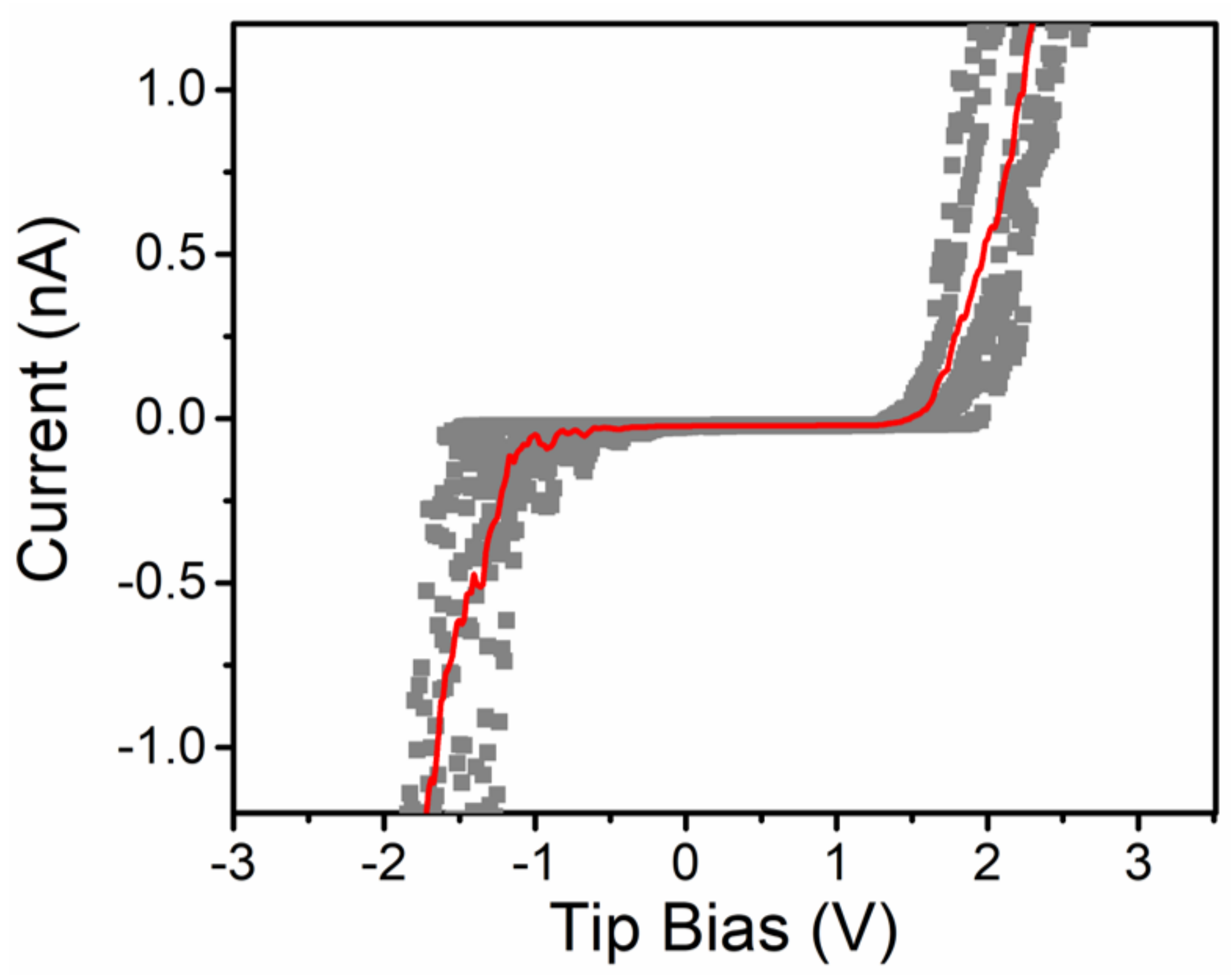
Tunneling transport through few layer hBN films was investigated using C-AFM. Figure 6 shows data from 9 I-V sweeps taken at 3 different spots across a sample. Across multiple spots the curves fall very closely to one another indicating the good uniformity of the film. The I-V curves show a small linear increase at low voltages due to tunneling followed by an exponential turn on beyond 1 V. At near zero voltages we determine a slope of 0.0015 nA/V corresponding to an average tunneling resistance of 133 kΩ-cm. Assuming a thickness of 2 nm (6 layers), these values fit very well with similar measurements on exfoliated flakes and films [40,41]. The high resistive nature indicates there potential usefulness for applications as insulating dielectric substrate without the need for transfer.
4. Summary
We have presented on MOCVD growth of multi-layer (3 to 8) hBN on Ni(111) from separate B(TEB) and N (NH3) precursors. Based on a collection of structural, chemical, and surface characterization techniques we find layers to be of excellent quality. Analysis of the geometry and orientation of hBN islands and edge features shows films are aligned to the substrate with the BN zigzag edge aligned to the <110> of Ni. Investigation of the growth process and surface chemistry reveals that when TEB is exposed to the surface first layered growth is disrupted, which is accompanied by the formation Ni-B and graphitic carbon upon this initial TEB exposure. Characterization of vertical electrical properties by C-AFM demonstrates films are high resistive (133 kΩ-cm) showing tunneling type conduction. This collective work demonstrates the feasibility of using MOCVD for growth of multi-layer hBN suitable as an insulating substrate without requiring transfer.
Author Contributions
G.S. and M.S. prepared the manuscript. G.S. grew samples, conducted characterization and analysis. G.G. and C.M. conducted XPS analysis. A.H. conducted electrical testing and analysis. M.S. planned research and preformed Raman analysis. All authors read and commented on the manuscript before submission.
Funding
This research was funded by the Air Force Office of Scientific Research under grant number FA9550-19RYCOR050.
Acknowledgments
The authors would like to thank Timothy Prusnick for his assistance with the collection and analysis of the Raman data. They would also like to thank the Utah NanoFab for their TEM and FIB contributions for this work.
Conflicts of Interest
The authors declare no conflict of interest.
References
- Gupta, A.; Sakthivel, T.; Seal, S. Recent development in 2D materials beyond graphene. Prog. Mater. Sci. 2015, 73, 44–126. [Google Scholar] [CrossRef]
- Kim, S.J.; Choi, K.; Kim, Y.; Hong, B.H. Materials for flexible, stretchable electronics: Graphene and 2D materials. Ann. Rev. Mater. Res. 2015, 45, 63–84. [Google Scholar] [CrossRef]
- Wang, Q.H.; Kalantar-Zadeh, K.; Kis, A.; Coleman, J.N.; Strano, M.S. Electronics and optoelectronics of two-dimensional transition metal dichalcogenides. Nat. Nanotechnol. 2012, 7, 699–712. [Google Scholar] [CrossRef] [PubMed]
- Novoselov, K.S.; Mishchenko, A.; Carvalho, A.; Castro Neto, A.H. 2D materials and van der Waals heterostructures. Science 2016, 353, aac9439. [Google Scholar] [CrossRef] [PubMed] [Green Version]
- Mas-Balleste, R.; Gomez-Navarro, C.; Gomez-Herrero, J.; Zamora, F. 2D materials: To graphene and beyond. Nanoscale 2011, 3, 20–30. [Google Scholar] [CrossRef] [PubMed]
- Dean, C.R.; Young, A.F.; Meric, I.; Lee, C.; Wang, L.; Sorgenfrei, S.; Watanabe, K.; Taniguchi, T.; Kim, P.; Shepard, L.K.; et al. Boron nitride substrates for high-quality graphene electronics. Nat. Nanotechnol. 2010, 5, 722–726. [Google Scholar] [CrossRef] [PubMed]
- Zomer, P.J.; Dash, S.P.; Tombros, N.; van Wees, B.J. A transfer technique for high mobility graphene devices on commercially available hexagonal boron nitride. Appl. Phys. Lett. 2011, 99, 232104. [Google Scholar] [CrossRef] [Green Version]
- Kobayashi, Y.; Kumakura, K.; Akasaka, T.; Makimoto, T. Layered boron nitride as a release layer for mechanical transfer of GaN-based devices. Nature 2012, 484, 223–227. [Google Scholar] [CrossRef]
- Levendorf, M.P.; Kim, C.-J.; Brown, L.; Huang, P.Y.; Havener, R.W.; Muller, D.A.; Park, J. Graphene and boron nitride lateral heterostructures for atomically thin circuitry. Nature 2012, 488, 627–632. [Google Scholar] [CrossRef]
- Shanmugam, M.; Jacobs-Gedrim, R.; Durcan, C.; Yu, B. 2D layered insulator hexagonal boron nitride enabled surface passivation in dye sensitized solar cells. Nanoscale 2013, 5, 11275–11282. [Google Scholar] [CrossRef]
- Zhang, J.; Yang, Y.; Lou, J. Investigation of hexagonal boron nitride as an atomically thin corrosion passivation coating in aqueous solution. Nanotechnology 2016, 27, 364004. [Google Scholar] [CrossRef] [PubMed]
- Doganov, R.A.; O’Farrell, E.C.T.; Koenig, S.P.; Yeo, Y.; Ziletti, A.; Carvalho, A.; Campbell, D.K.; Coker, D.F.; Watanabe, K.; Taniguchi, T.; et al. Transport properties of pristine few-layer black phosphorus by van der Waals passivation in an inert atmosphere. Nat. Commun. 2015, 6, 6647. [Google Scholar] [CrossRef] [PubMed]
- Song, L.; Ci, L.; Lu, H.; Sorokin, P.B.; Jin, C.; Ni, J.; Kvashnin, A.G.; Kvashnin, D.G.; Lou, J.; Yakobson, B.I.; et al. Large scale growth and characterization of atomic hexagonal boron nitride layers. Nano Lett. 2010, 10, 3209–3215. [Google Scholar] [CrossRef] [PubMed]
- Lee, K.H.; Shin, H.-J.; Lee, J.; Lee, I.; Kim, G.-H.; Choi, J.-Y.; Kim, S.-W. Large-scale synthesis of high-quality hexagonal boron nitride nanosheets for large-area graphene electronics. Nano Lett. 2012, 12, 714–718. [Google Scholar] [CrossRef] [PubMed]
- Kubota, Y.; Watanabe, K.; Tsuda, O.; Taniguchi, T. Hexagonal boron nitride single crystal growth at atmospheric pressure using Ni-Cr solvent. Chem. Mater. 2008, 20, 1661–1663. [Google Scholar] [CrossRef]
- Vuong, T.Q.P.; Cassabois, G.; Valvin, P.; Rousseau, E.; Summerfield, A.; Mellor, C.J.; Cho, Y.; Cheng, T.S.; Albar, J.D.; Eaves, L.; et al. Deep ultraviolet emission in hexagonal boron nitride grown by high-temperature molecular beam epitaxy. 2D Mater. 2017, 4, 021023. [Google Scholar] [CrossRef]
- Li, L.H.; Chen, Y.; Behan, G.; Zhang, H.; Petravic, M.; Glushenkov, A.M. Large-scale mechanical peeling of boron nitride nanosheets by low-energy ball milling. J. Mater. Chem. 2011, 21, 11862–11866. [Google Scholar] [CrossRef]
- Zhang, K.; Feng, Y.; Wang, F.; Yang, Z.; Wang, J. Two dimensional hexagonal boron nitride (2D-hBN): Synthesis, properties and applications. J. Mater. Chem. C 2017, 5, 11992–12022. [Google Scholar] [CrossRef]
- Yasui, H.; Awazu, K.; Ikenaga, N.; Sakudo, N. Synthesis and characterization of BN thin films prepared by plasma MOCVD with organoboron precursors. Vacuum 2008, 83, 582–584. [Google Scholar] [CrossRef]
- Siegel, G.; Ciobanu, C.V.; Narayanan, B.; Snure, M.; Badescu, S.C. Heterogeneous pyrolysis: A route for epitaxial growth of hBN atomic layers on copper using separate boron and nitrogen precursors. Nano Lett. 2017, 17, 2404–2413. [Google Scholar] [CrossRef]
- Chen, Y.; Liang, H.; Xia, X.; Zhang, H.; Shi, J.; Abbas, Q.; Du, G. Growth temperature impact on film quality of hBN grown on Al2O3 using non-catalyzed borazane CVD. J. Mater. Sci. Mater. Electron. 2017, 28, 14341–14347. [Google Scholar] [CrossRef]
- Stehle, Y.; Meyer, H.M., III; Unocic, R.R.; Kidder, M.; Polizos, G.; Datskos, P.G.; Jackson, R.; Smirnov, S.N.; Vlassiouk, I.V. Synthesis of hexagonal boron nitride monolayer: Control of nucleation and crystal morphology. Chem. Mater. 2015, 27, 8041–8047. [Google Scholar] [CrossRef]
- Kim, K.K.; Hsu, A.; Jia, X.; Kim, S.M.; Shi, Y.; Hofmann, M.; Nezich, D.; Rodriguez-Nieva, J.F.; Dresselhaus, M.; Palacios, T.; et al. Synthesis of monolayer hexagonal boron nitride on Cu foil using chemical vapor deposition. Nano Lett. 2012, 12, 161–166. [Google Scholar] [CrossRef] [PubMed]
- Goriachko, A.; Knapp, M.; Over, H. Self-assembly of a hexagonal boron nitride nanomesh on Ru(0001). Langmuir 2007, 23, 2928–2931. [Google Scholar] [CrossRef] [PubMed]
- Liu, Z.; Song, L.; Zhao, S.; Huang, J.; Ma, L.; Zhang, J.; Lou, J.; Ajayan, P.M. Direct growth of graphene/hexagonal boron nitride stacked layers. Nano Lett. 2011, 11, 2032–2037. [Google Scholar] [CrossRef]
- Liu, L.; Park, J.; Siegel, D.A.; McCarty, K.F.; Clark, K.W.; Deng, W.; Basile, L.; Idrobo, J.C.; Li, A.-P.; Gu, G. Heteroepitaxial growth of two-dimensional hexagonal boron nitride templated by graphene edges. Science 2014, 343, 163–167. [Google Scholar] [CrossRef]
- Kim, S.M.; Hsu, A.; Araujo, P.T.; Lee, Y.-H.; Palacios, T.; Dresselhaus, M.; Idrobo, J.-C.; Kim, K.K.; Kong, J. Synthesis of patched or stacked graphene and hBN flakes: A route to hybrid structure discovery. Nano Lett. 2013, 13, 933–941. [Google Scholar] [CrossRef]
- Hubacek, M.; Sato, T. The effect of copper on the crystallization of hexagonal boron nitride. J. Mater. Sci. 1997, 32, 3293–3297. [Google Scholar] [CrossRef]
- Ismach, A.; Chou, H.; Ferrer, D.A.; Wu, Y.P.; McDonnell, S.; Floresca, H.C.; Covacevich, A.; Pope, C.; Piner, R.; Kim, M.J.; et al. Towards the controlled synthesis of hexagonal boron nitride films. ACS Nano 2012, 6, 6378–6385. [Google Scholar] [CrossRef]
- Ebnonnasir, A.; Kodambaka, S.; Ciobanu, C.V. Strongly and weakly interacting configurations of hexagonal boron nitride on nickel. Surf. Rev. Lett. 2015, 22, 1550078. [Google Scholar] [CrossRef]
- Snure, M.; Vangala, S.; Shoaf, J.; Hu, J.; Paduano, Q. Influence of Cu film microstructure on MOCVD growth of BN. In Proceedings of the MRS, Boston, MA, USA, 29 November 2015; p. 1726. [Google Scholar]
- Kim, S.M.; Hsu, A.; Park, M.H.; Chae, S.H.; Yun, S.J.; Lee, J.S.; Cho, D.H.; Fang, W.J.; Lee, C.; Palacios, T.; et al. Synthesis of large-area multilayer hexagonal boron nitride for high material performance. Nat. Commun. 2015, 6, 8662. [Google Scholar] [CrossRef] [PubMed]
- Li, X.; Sundaram, S.; Gmili, Y.E.; Ayari, T.; Puybaret, R.; Patriarche, G.; Voss, P.L.; Salvestrini, J.P.; Ougazzaden, A. Large-area two-dimensional layered hexagonal boron nitride grown on sapphire by metalorganic vapor phase epitaxy. Cryst. Growth Des. 2016, 16, 3409–3415. [Google Scholar] [CrossRef]
- Chubarov, M.; Pedersen, H.; Hogberg, H.; Jensen, J.; Henry, A. Growth of high quality epitaxial rhombohedral boron nitride. Cryst. Growth Des. 2012, 12, 3215–3220. [Google Scholar] [CrossRef]
- Jeong, H.; Kim, D.Y.; Kim, J.; Moon, S.; Han, N.; Lee, S.H.; Okello, O.F.N.; Song, K.; Choi, S.-Y.; Kim, J.K. Wafer-scale and selective-area growth of high-quality hexagonal boron nitride on Ni(111) by metal-organic chemical vapor deposition. Sci. Rep. 2019, 9, 5736. [Google Scholar] [CrossRef] [PubMed]
- Kobayashi, Y.; Akasaka, T.; Makimoto, T. Hexagonal boron nitride grown by MOVPE. J. Cryst. Growth 2008, 310, 5048–5052. [Google Scholar] [CrossRef]
- Li, X.; Cai, W.; An, J.; Kim, S.; Nah, J.; Yang, D.; Piner, R.; Velamakanni, A.; Jung, I.; Tutuc, E.; et al. Large-area synthesis of high-quality and uniform graphene films on copper foils. Science 2009, 324, 1312–1314. [Google Scholar] [CrossRef]
- Lee, G.H.; Yu, Y.J.; Lee, C.; Dean, C.; Shepard, K.L.; Kim, P.; Hone, J. Electron tunneling through atomically flat and ultrathin hexagonal boron nitride. App. Phys. Lett. 2011, 99, 243114. [Google Scholar] [CrossRef] [Green Version]
- Glavin, N.R.; Jespersen, M.L.; Check, M.H.; Hu, J.; Hilton, A.M.; Fisher, T.S.; Voevdin, A.A. Synthesis of few-layer, large area hexagonal-boron nitride by pulsed laser deposition. Thin Solid Films 2014, 572, 245–250. [Google Scholar] [CrossRef]
- Auwärter, W. Hexagonal boron nitride monolayers on metal supports: Versatile templates for atoms, molecules and nanostructures. Surf. Sci. Rep. 2018, 74, 1–95. [Google Scholar] [CrossRef]
- Shi, Y.; Hamsen, C.; Jia, X.; Kim, K.K.; Reina, A.; Hofmann, M.; Hsu, A.L.; Zhang, K.; Li, H.; Juang, Z.-Y.; et al. Synthesis of few-layer hexagonal boron nitride thin film by chemical vapor deposition. Nano Lett. 2010, 10, 4134–4139. [Google Scholar] [CrossRef]
Figure 1.
hBN hilms on Ni(111). (a) Raman spectrum of an as-grown hBN few layer film on Ni(111). (b) Raman spectrum of an hBN film transferred to SiO2/Si substrate. (c) High-resolution XPS of the N 1s and B 1s peaks of an as-grown hBN on Ni(111) film. (d) Atomic force microscopy (AFM) image of the surface of a hBN on Ni(111) film. (e) TEM cross-sectional image of hBN on Ni(111).

Figure 2.
Alignment and stacking of hBN/Ni(111) films. (a) AFM height map image of hBN on Ni(111). (b) Phase image of the height map shown in (a). (c) Histogram of edge alignment of the triangular hBN grains. (d) Schematic showing stacking of hBN on Ni(111) having very close alignment.
Figure 2.
Alignment and stacking of hBN/Ni(111) films. (a) AFM height map image of hBN on Ni(111). (b) Phase image of the height map shown in (a). (c) Histogram of edge alignment of the triangular hBN grains. (d) Schematic showing stacking of hBN on Ni(111) having very close alignment.

Figure 3.
Surface analysis of hBN/Ni films vs growth time. (a) 1 min. growth height map. (b) 15 min. growth height map. (c) 30 min. growth height map. (d) 60 min. growth height map. (e) 1 min. growth phase map. (f) 15 min. growth phase map. (g) 30 min. growth phase map. (h) 60 min. growth phase map.

Figure 4.
Characterization of early exposure of individual precursors. (a) AFM image of a triethylborane (TEB) pre-exposed sample. (b) Raman spectrum of a TEB pre-exposed sample. (c) AFM image of a NH3 pre-exposed sample. (d) Raman spectrum of a NH3 pre-exposed sample.
Figure 4.
Characterization of early exposure of individual precursors. (a) AFM image of a triethylborane (TEB) pre-exposed sample. (b) Raman spectrum of a TEB pre-exposed sample. (c) AFM image of a NH3 pre-exposed sample. (d) Raman spectrum of a NH3 pre-exposed sample.
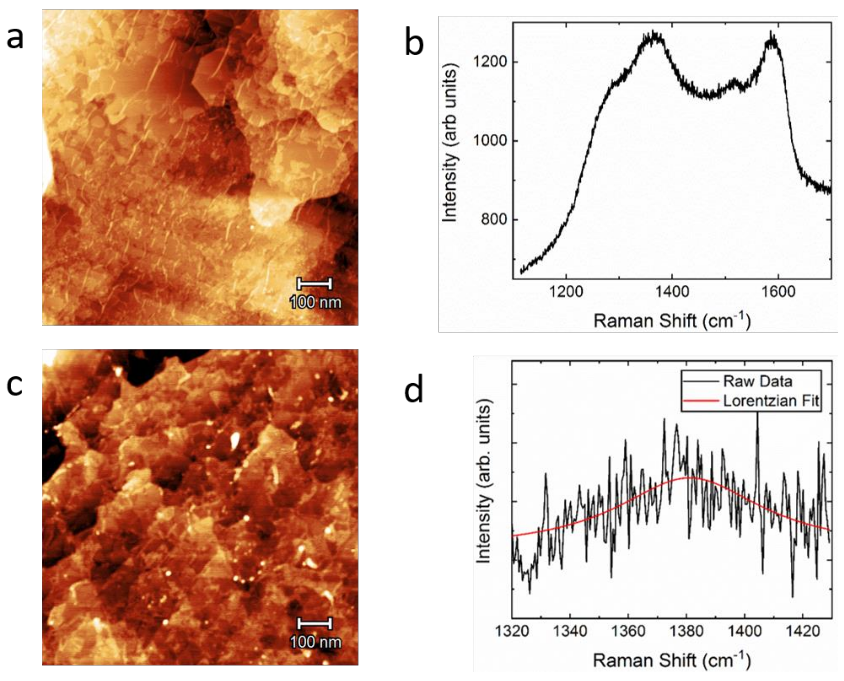
Figure 5.
XPS analysis of single precursor growths. (a) B 1s peak for a TEB growth. (b) N 1s data for a TEB growth. (c) C 1s peak for a TEB growth. (d) B 1s peak for a NH3 growth. (e) N 1s peak for a NH3 growth. (f) C 1s peak for a NH3 growth.
Figure 5.
XPS analysis of single precursor growths. (a) B 1s peak for a TEB growth. (b) N 1s data for a TEB growth. (c) C 1s peak for a TEB growth. (d) B 1s peak for a NH3 growth. (e) N 1s peak for a NH3 growth. (f) C 1s peak for a NH3 growth.

Figure 6.
I-V curves from conductive-probe AFM (C-AFM) measurements. Curves in gray are from nine different measurements at three different spots on a sample. The red curve is the average of the gray curves.
Figure 6.
I-V curves from conductive-probe AFM (C-AFM) measurements. Curves in gray are from nine different measurements at three different spots on a sample. The red curve is the average of the gray curves.
© 2019 by the authors. Licensee MDPI, Basel, Switzerland. This article is an open access article distributed under the terms and conditions of the Creative Commons Attribution (CC BY) license (http://creativecommons.org/licenses/by/4.0/).
Share and Cite
MDPI and ACS Style
Siegel, G.; Gryzbowcki, G.; Hilton, A.; Muratore, C.; Snure, M. Growth of Multi-Layer hBN on Ni(111) Substrates via MOCVD. Crystals 2019, 9, 339. https://doi.org/10.3390/cryst9070339
AMA Style
Siegel G, Gryzbowcki G, Hilton A, Muratore C, Snure M. Growth of Multi-Layer hBN on Ni(111) Substrates via MOCVD. Crystals. 2019; 9(7):339. https://doi.org/10.3390/cryst9070339
Chicago/Turabian StyleSiegel, Gene, Gordon Gryzbowcki, Albert Hilton, Christopher Muratore, and Michael Snure. 2019. "Growth of Multi-Layer hBN on Ni(111) Substrates via MOCVD" Crystals 9, no. 7: 339. https://doi.org/10.3390/cryst9070339
Note that from the first issue of 2016, this journal uses article numbers instead of page numbers. See further details here.