Crystal Structures of GaN Nanodots by Nitrogen Plasma Treatment on Ga Metal Droplets


Department of Materials Science and Engineering, National Dong Hwa University, Hualien 97401, Taiwan
*
Author to whom correspondence should be addressed.
Metals 2018, 8(6), 419; https://doi.org/10.3390/met8060419
Submission received: 20 April 2018
/
Revised: 30 May 2018
/
Accepted: 30 May 2018
/
Published: 4 June 2018
(This article belongs to the Special Issue Plasmas Processes Applied on Metals and Alloys)
Abstract
:Gallium nitride (GaN) is one of important functional materials for optoelectronics and electronics. GaN exists both in equilibrium wurtzite and metastable zinc-blende structural phases. The zinc-blende GaN has superior electronic and optical properties over wurtzite one. In this report, GaN nanodots can be fabricated by Ga metal droplets in ultra-high vacuum and then nitridation by nitrogen plasma. The size, shape, density, and crystal structure of GaN nanodots can be characterized by transmission electron microscopy. The growth parameters, such as pre-nitridation treatment on Si surface, substrate temperature, and plasma nitridation time, affect the crystal structure of GaN nanodots. Higher thermal energy could provide the driving force for the phase transformation of GaN nanodots from zinc-blende to wurtzite structures. Metastable zinc-blende GaN nanodots can be synthesized by the surface modification of Si (111) by nitrogen plasma, i.e., the pre-nitridation treatment is done at a lower growth temperature. This is because the pre-nitridation process can provide a nitrogen-terminal surface for the following Ga droplet formation and a nitrogen-rich condition for the formation of GaN nanodots during droplet epitaxy. The pre-nitridation of Si substrates, the formation of a thin SiNx layer, could inhibit the phase transformation of GaN nanodots from zinc-blende to wurtzite phases. The pre-nitridation treatment also affects the dot size, density, and surface roughness of samples.
1. Introduction
Group-III nitride-based semiconductors (InN, GaN, and AlN) have very wide bandgaps from 0.64 to 6.2 eV for various applications in optoelectronics and electronics [1]. Gallium nitride, with a direct bandgap of 3.4 eV, which shows high carrier mobility and high thermal conductivity, has been successful applied in commercialized devices, such as light emitting diodes (LED) and high electron mobility transistors (HEMT) [2,3]. Moreover, for the quantum computing applications, nanostructures of GaN have large exciton binding energy and confinement potential for devices, such as single-photon emitters [4] and single-electron transistors [5]. In particular, GaN quantum dots are promising materials in these devices [6].
For the fabrication techniques of GaN, GaN thin films can be epitaxially grown by molecular beam epitaxy (MBE), metal-organic chemical vapor deposition (MOCVD), pulsed laser deposition (PLD), and Hydride vapor-phase epitaxy (HVPE) [7,8,9,10,11]. Once the epi-layers have the lattice mismatch with two-dimensional wetting layers or substrates, self-assembled GaN nanodots can form due to the strain relaxation; this method is called the Stranski-Krastanov (SK) mode of epitaxial growth [12,13]. Among these techniques, MBE procedure is performed in an ultra-high vacuum chamber in order to minimize contamination and in a lower-temperature growth condition. Other advantages of MBE are its capability to create heterostructures with sharp interfaces, and also to form metastable phase as zinc-blende structure of GaN. For another growth method of semiconductor nanostructures, droplet epitaxy mode using an MBE system was first proposed by Koguchi in 1990 [14,15]. Therefore, the study of droplet epitaxy technique for GaN nanodots was initiated, which is the method of first forming Ga metal droplets in ultra-high vacuum, followed by the treatment of a nitrogen plasma source [16]. There are some advantages of droplet epitaxy by plasma-assisted MBE systems. For instance, self-organized GaN nanodots can be grown directly on various substrates. Density of GaN nanodots can be controlled by the growth parameters. Metastable zinc-blende structure can be performed in the GaN nanodots on sapphires by droplet epitaxy [17,18,19,20].
For the crystal structure of GaN nanostructures, wurtzite GaN is the thermodynamically stable phase, which suffers from the presence of a large built-in electric field, called the quantum confined Stark effect, that may degrade the device performance [21,22]. On the other hand, the metastable zinc-blende (cubic) phase of GaN has no polarization fields. The polarization field effect, called the piezoelectric field effect, significantly affects the band structures and optical gain of optoelectronic devices. The radiative recombination time of cubic GaN quantum dots is two orders of magnitude higher than the one for wurtzite GaN quantum dots. The mobility of electrons and holes in a zinc-blende GaN is also intrinsically higher than in a wurtzite GaN due to lower phonon scattering in cubic crystals [23]. Up to now, most of the reports on the growth of cubic GaN nanodots have been proposed by the method of SK mode [24,25,26]. For the growth mode of droplet epitaxy, Wang et al. reported the mixture phases of wurtzite and zinc-blende on a sapphire substrate at the substrate temperature of 710 °C [18]. As’s group reported cubic GaN quantum dots grown on 3C-AlN (001) substrates [27]. Studies on the phase transformation of GaN nanodots on silicon by droplet epitaxy technique are still rare. In this work, we focus on the investigation the crystal structures of GaN nanodots on Si (111) substrates fabricated by nitrogen plasma nitridation on the Ga metal droplets. The microstructure and crystal structures of GaN nanodots were characterized by transmission electron microscopy (TEM). The growth parameters of GaN nanodots, such as substrate temperatures and surface pre-nitridation treatment, influence on the crystal phases of GaN nanodots. Nonpolar GaN nanodots with cubic crystal structure can be performed on Si substrates by droplet epitaxy for the future applications in solid state quantum devices.
2. Materials and Methods
GaN nanodots grown by the method of droplet epitaxy were carried out in our ULVAC MBE system with a radio frequency (RF) nitrogen plasma source [19]. Two inch Si (111) wafers were cleaned using acetone to remove organic impurities and using 10% HF solution to remove the native oxide. After the chemical cleaning, one Si wafer was immediately put into MBE chamber with the base pressure of 1.0 × 10⁻⁷ Pa. Then, Si substrates were heated to the temperature 850 °C for 20 min. After the thermal cleaning, the temperature of Si substrate was set to 500 or 550 °C for droplet epitaxy. For the droplet epitaxy process, nanoscale Ga metal droplets were initially formed on Si substrate at beam equivalent pressure 1.9 × 10⁻⁴ Pa for the duration of 1 min by a Knudsen cell with 99.999999% Ga metal. Ga adatoms had high sticking coefficients on the substrate at lower growth temperature. At elevated temperatures, surface Ga accumulation was less effective since Ga atoms can evaporate from the surface [28]. The accumulation of Ga atoms had high surface free energy to form nanoscale Ga droplets according to the Volmer-Weber (VW) growth model [29]. Subsequently, the droplets were converted into GaN nanodots by using a nitrogen plasma source, called nitridation process. The parameters of nitridation were operated at an RF forward power of 500 W and N2 flux of 2 sccm for 5 or 10 min. In addition, the pre-nitridation treatment at temperature 600 °C for 60 min on Si wafers was optionally conducted before the thermal evaporation of Ga metal droplets. The growth parameters of four samples are summarized in Table 1. MBE system was equipped with an in-situ reflection high-energy electron diffraction (RHEED), which was employed for the observation of surface condition during the process of droplet epitaxy. RHEED patterns of samples C1 and C2 are shown in Figure 1. The flat and reconstructed Si (111) surfaces can be obtained after thermal cleaning in Figure 1a,d, which showed long-streak patterns. After the pre-nitridation treatment on Si, the RHEED patterns changed from striped to foggy due to the formation of amorphous nitride layer on Si, shown in Figure 1b. After the formation of Ga droplets, the pattern of surface was still foggy (not shown) which indicated an amorphous structure on the surface. Then, nitridation process led to the formation of GaN nanodots which showed the ring-centered pattern in Figure 1c. For the sample without the pre-nitridation process (C2), the RHEED pattern became foggy after the formation of Ga droplets, shown in Figure 1e. After the nitridation process, the formation of GaN nanodots also showed the ring-centered pattern in Figure 1f, indicating the polycrystalline GaN nanodots on Si [30].
After the formation of GaN nanodots, surface morphology of the samples was examined using the images generated by field-emission scanning electron microscopy (SEM, JSE-7000F, JEOL, Tokyo, Japan) with accelerating voltage 15 KV. According to the observation of SEM, densities of GaN nanodots could be obtained. The surface roughness of samples was investigated by atomic force microscopy (AFM, C3000, Nanosurf, Liestal, Switzerland). The surface chemical composition of samples was studied by X-ray photoelectron spectroscopy (XPS, K-Alpha, Thermo Scientific, Waltham, MA, USA). For the observation of GaN nanodots microstructure and crystal structures, high-resolution TEM images, and selective-area diffraction patterns were performed by using JEOL JEM-3010 with accelerating voltage 300 KV. The TEM specimen were prepared by Ar ion milling with an accelerating voltage of 5 KeV for the cross-section and plane-view TEM observations.
3. Results and Discussion
In the left column of Figure 2, SEM images showed GaN nanodots on the surface of Si (111) in the magnification of 50,000, and their densities in the area of 5.65 μm2 were calculated from the SEM images as 5.72 × 1010 cm−2, 2.57 × 1010 cm−2, 5.61 × 1010 cm−2, and 5.01 × 1010 cm−2 for samples C1, C2, C3, and C4. To compare C1 with C2 or C3 with C4, the pre-nitridation treatment of Si surface made the density of GaN nanodots increase. C1 and C3 samples with pre-nitridation had higher density than the C2 and C4 samples without pre-nitridation, respectively. Moreover, the cross-section TEM images of GaN nanodots in the range of 500 nm are shown in the right column of Figure 2. The average diameters of GaN nanodots were calculated from the TEM images as 21.9 nm, 24.5 nm, 15.1 nm, and 18.3 nm for C1, C2, C3, and C4, respectively. The pre-nitridation treatment made the size of GaN nanodots decrease slightly. In brief, the surface conditions of Si (111) can be modified by the substrate pre-nitridaiton process, as shown in the observation of in-situ RHEED, the nitrogen-terminal surface could influence the sticking coefficient of Ga atoms or the surface diffusion of Ga atoms. The surface-sticking coefficients of Ga atoms over N atoms can be higher than Ga atoms over Si atoms according to the chemical surface stability. The stronger bonding could reduce the surface diffusion length of Ga atoms during the formation of Ga droplets [31,32]. Therefore, we found an increase of density and a decrease of average diameter of GaN nanodots for the samples with nitrogen plasma pre-nitridation treatment (C1 and C3).
To further analyze their surface roughness, AFM images in an area of 5 μm × 5 μm of four samples are shown in Figure 3. The average roughness of samples C1, C2, C3, and C4 are 2.56, 3.04, 1.34, and 1.65 nm, respectively. The samples without pre-nitridation treatment (C2 or C4) had higher surface roughness value than the ones with pre-nitridation (C1 or C3). This is because the larger size and lower density of GaN nanodots on Si which can perform higher surface roughness of samples. The observation of AFM was consistent to the results of SEM and TEM in Figure 2.
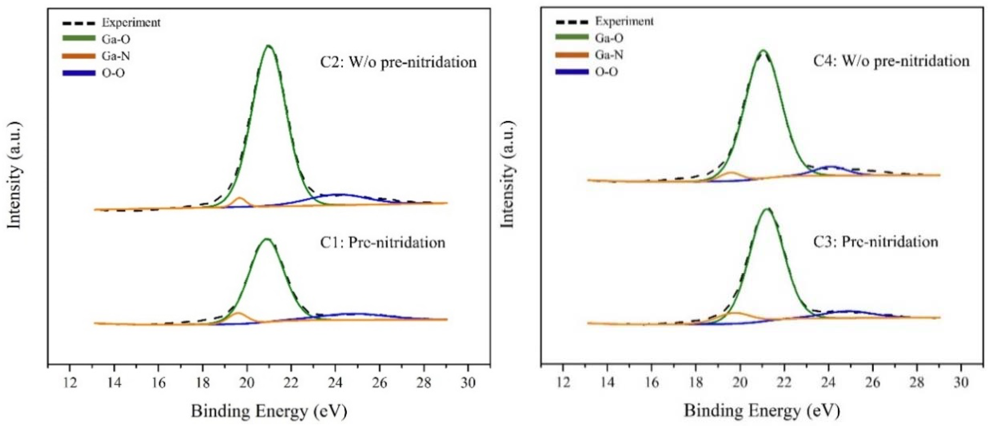
Since the pre-nitirdation treatment of Si (111) influenced the growth of GaN nanodots, we went forward to investigate the surface chemical composition using the measurements of XPS. Figure 4 shows the de-convoluted Ga-3d XPS spectra of GaN nanodots on Si (111) for samples C1, C2, C3, and C4. The XPS spectra were divided into three major components: Ga–O bonding with peak energy around 20.7 eV, Ga–N bonding with peak energy around 19.7 eV, and O–O bonding with the peak energy around 25.0 eV, obtained using the software Thermo Avantage (version 4, Thermo Scientific, Waltham, MA, USA). The samples with pre-nitridation treatment (C1 and C3) had relatively stronger peak intensities of Ga–N bonding due to more nitrogen provided for the formation of GaN nanodots. Meanwhile, we found high amount of oxygen chemisorptions on the surface of samples [33]. The strong Ga–O and weak O–O bonds came from the oxidation of nanodots on exposure to the air due to strong difference the electro negativity between Ga and O atoms [21]. This was because the uncompleted crystallization of Ga metal droplets could have existed after nitrogen plasma nitridation. When the nitridation time increased for samples C3 and C4, the peak intensity of Ga–N bonding was stronger due to the formation of the GaN crystal being more complete.
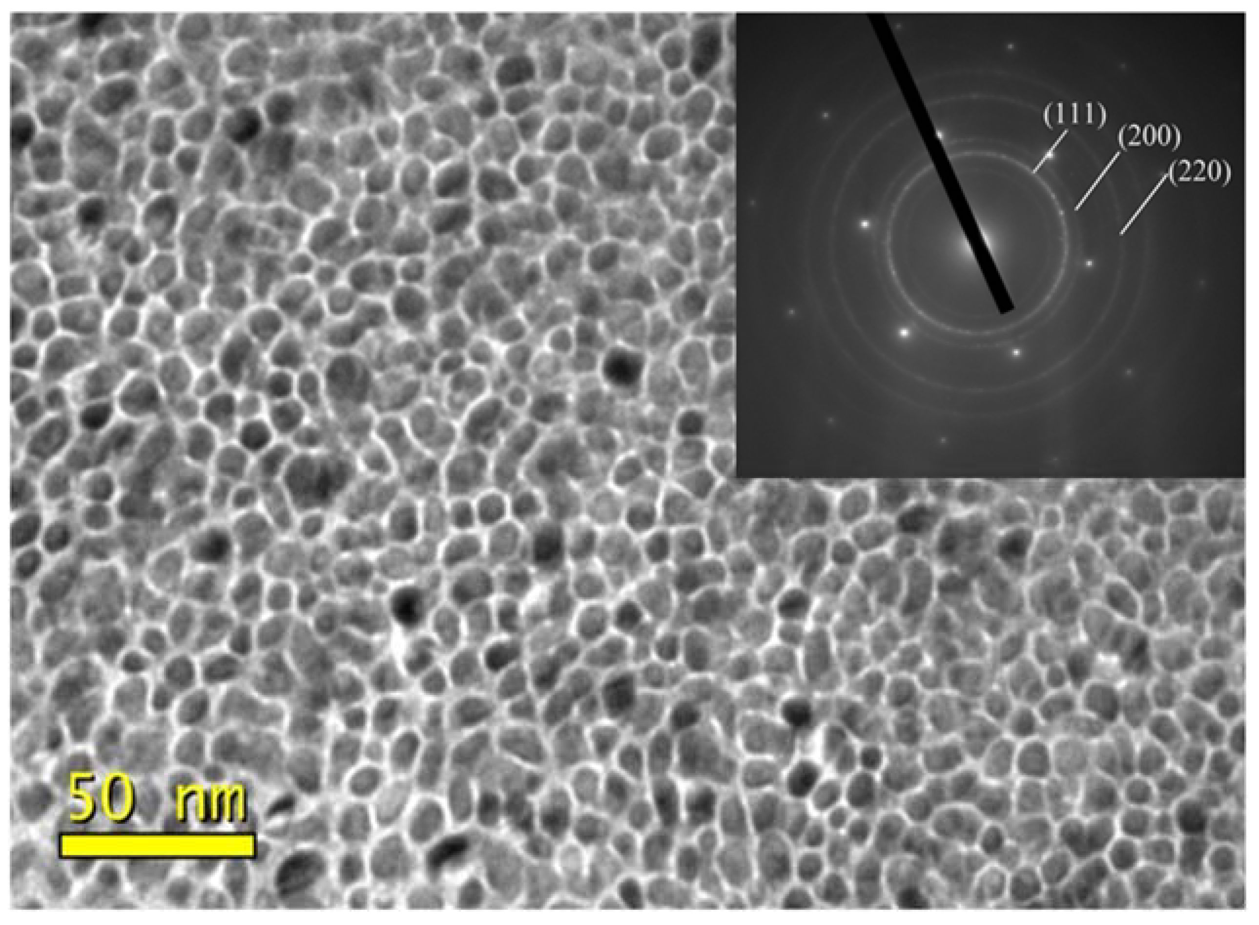
In order to identify the crystal structures of GaN nanodots, we prepared the specimens for the cross-section images of high-resolution transmission electron microscopy (HRTEM) and analyzed the crystal planes using the software Digital Micrograpy (version 1, Gatan, Pleasanton, CA, USA). The fast Fourier transformation (FFT) of the original HRTEM images was conducted on a single GaN nanodot, which can provide the simulated diffraction patterns. And then, the inverse fast Fourier transformation (IFFT) of the simulated diffraction patterns provided a clearer crystal structure of a single GaN nanodot. Finally, crystal planes can be identified according to the database of software [34]. Moreover, for the TEM observations of multiple GaN nanodots, we prepared the specimens for plane-view TEM images as shown in Figure 5 and analyzed the selective area diffraction (SAD) patterns of GaN nanodots at a magnification of 500,000. The d-space of ring-like patterns can provide the planes for each ring using the software CSpot (version 1, CrystOrient, Zabierzów, Poland) with the aid of a crystallography open database [35]. Figure 5 shows the plane-view TEM image of sample C1 and its ring-like diffraction pattern in the inset. The ring-like pattern came from the polycrystalline GaN nanodots, which was consistent with the results of RHEED observations. In the TEM images, we could also find that the individual GaN dot could contain different misoriented nano-crystals.
Figure 6a,b shows cross-section HRTEM images of a single GaN nanodot, and Figure 6c,d shows the SAD patterns of GaN nanodots for samples C1 and C2, respectively. According to the analysis using TEM software, the crystal planes of a single GaN nanodot could be identified, and the phase of GaN nanodots could be investigated by the polycrystalline ring-like patterns. For the sample C1, the (200) plane of zinc-blende GaN is shown in Figure 6a, and the cubic structure of GaN nanodots with planes (111), (200), and (220) is shown in Figure 6c. Cubic GaN nanodots could be obtained on Si (111) by the growth parameters of sample C1. On the contrary, we verified the TEM images of sample C2. The (101) and (002) planes of wurtzite structure are shown in Figure 6b, and the ring patterns with planes (100), (002) and (101) for the wurtzite crystal structure of GaN nanodots are shown in Figure 6d. According to the TEM results of samples C1 and C2, the pre-nitridation treatment on Si (111) could inhibit the phase transformation from metastable zinc-blende to stable wurtzite structures. For the microstructures of GaN films grown by MBE, the nitrogen-rich growth condition showed the existence of zinc-blende GaN phase [36]. The pre-nitridation treatment could serve as a larger nitrogen source for the formation of GaN nanodots. Therefore, the cubic GaN nanodots dominated in the sample C1.
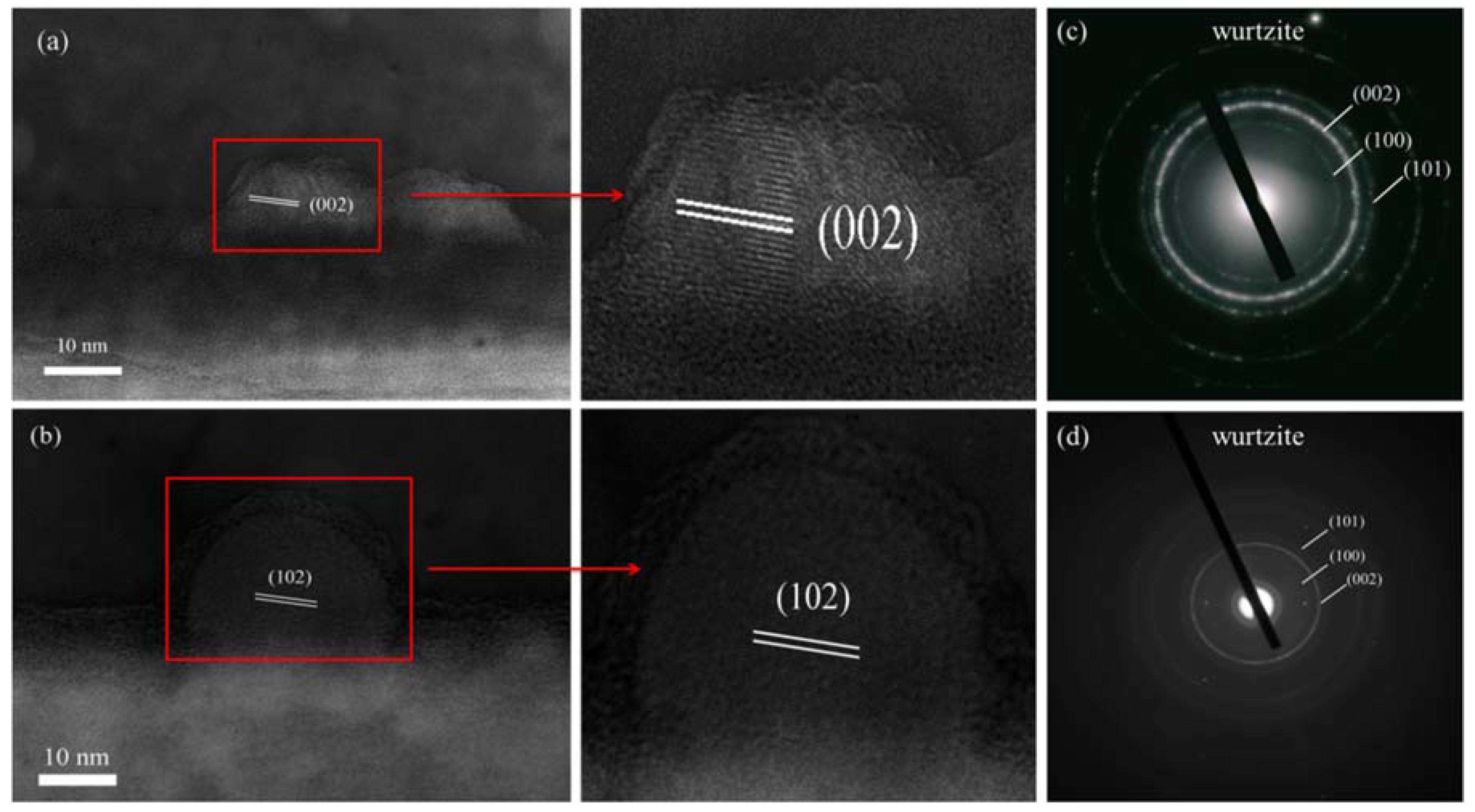
To further investigate the effect of thermal budget on the crystal structures of GaN nanodots, Figure 7a,b shows cross-section HRTEM images of a single GaN nanodot, and Figure 7c,d shows the SAD patterns of GaN nanodots for samples C3 and C4, respectively. The (002) and (102) planes of wurtzite structure are shown in Figure 7a,b, and the ring-like patterns with planes (100), (002) and (101) both show the wurtzite crystal structure of GaN nanodots in Figure 7c,d. The higher substrate temperature of droplet epitaxy could lead to GaN nanodots phase transformation to wurtzite crystal structure. When the substrate temperature was raised during droplet epitaxy, high surface migration occurred, which improved the quality of the growth front of GaN and it became favorable to form the more thermodynamically equilibrated wurtzite phase [31,36].
4. Conclusions
GaN nanodots were fabricated on Si (111) by droplet epitaxy using a nitrogen plasma-assisted MBE system. Polycrystalline GaN nanodots were shown by the characterizations of in-situ RDEED and TEM. Uncompleted crystallization of the Ga metal droplets were observed from the measurement using XPS. The phase transformation of GaN nanodots from metastable zinc-blende crystal structure to stable wurtzite crystal structure could be inhibited by the surface modification of nitrogen plasma (i.e., pre-nitridation treatment). The pre-nitridation treatment also influenced the size and density of GaN nanodots. The nitrogen-terminal Si surface could not only change the sticking coefficient or the surface diffusion of Ga atoms, but also could provide the nitrogen-rich condition for the existence of zinc-blende phase. On the other hand, the stable wurtzite structure of GaN nandots could be found at higher growth temperatures. This was because the phase transformation of crystal structures depended on the activation free energy barrier. The higher temperature growth could decrease the energy barrier of phase transformation. In this report, we focused on the investigation of GaN-nanodot crystal structures. Nonpolar GaN nanodots with cubic crystal structure could be synthesized during the process of droplet epitaxy, which could have future applications of GaN nanodots for solid state quantum devices.
Author Contributions
I.-S.Y. designed the experiments and wrote the manuscript; Y.-Z.S. performed the experiments and analyzed the data.
Funding
This research was funded by Ministry of Science and Technology Taiwan (MOST 106-2221-E-259-010) and ULVAC Taiwan (NDHU 106A605).
Acknowledgments
The authors acknowledge Ministry of Science and Technology Taiwan and ULVAC Taiwan for financially supporting this study and publication. The authors also would like to acknowledge Micheal Chen and Stanley Wu of ULVAC Taiwan for the maintenance of PA-MBE system.
Conflicts of Interest
The authors declare no conflicts of interest.
References
- Wu, J. When group-III nitrides go infrared: New properties and perspectives. J. Appl. Phys. 2009, 106, 011101. [Google Scholar] [CrossRef]
- Nakamura, S.; Pearton, S.; Fasol, G. The Blue Laser Diode, 2nd ed.; Springer: Berlin, Germany, 2000. [Google Scholar]
- Su, M.; Chen, C.; Rajan, S. Prospects for the application of GaN power devices in hybrid electric vehicle drive systems. Semicond. Sci. Technol. 2013, 28, 074012. [Google Scholar] [CrossRef]
- Kako, S.; Holmes, M.; Sergent, S.; Burger, M.; As, D.J.; Arakawa, Y. Single-photon emission from cubic GaN quantum dots. Appl. Phys. Lett. 2014, 104, 011101. [Google Scholar] [CrossRef]
- Chou, H.T.; Goldhaber-Gordon, D.; Schmult, S.; Manfra, M.J.; Sergent, A.M.; Molnar, R.J. Single-electron transistors in GaN/AlGaN heterostructures. Appl. Phys. Lett. 2006, 89, 033104. [Google Scholar] [CrossRef]
- D’Amico, I.; Biolatti, E.; Rossi, F.; Derinaldis, S.; Rinaldis, R.; Cingolani, R. GaN quantum dot based quantum information/computing processing. Superlattices Microstruct. 2002, 31, 117–125. [Google Scholar] [CrossRef]
- Novikov, S.V.; Kent, A.J.; Foxon, C.T. Molecular beam epitaxy as a growth technique fpr achieving free-standing zinc-blende GaN and wurtzite AlxGa1−xN. Prog. Cryst. Growth Charact. Mater. 2017, 63, 25–39. [Google Scholar] [CrossRef]
- Susanto, I.; Kan, K.Y.; Yu, I.S. Temperature effects for GaN films grown on 4H-SiC substrate with 40 miscutting orientation by plasma-assisted molecular beam epitaxy. J. Alloys Compd. 2017, 723, 21–29. [Google Scholar] [CrossRef]
- Nakamura, S. GaN growth using GaN buffer layer. Jpn. J. Appl. Phys. 1991, 30, L1705–L1707. [Google Scholar] [CrossRef]
- Sudhir, G.S.; Fujii, H.; Wong, W.S.; Kisielowski, C.; Newman, N.; Dieker, C.; Liliental-Weber, Z.; Rubin, M.D.; Weber, E.R. Pulsed laser deposition of aluminum nitride and gallium nitride thin films. Appl. Surf. Sci. 1998, 127–129, 471–476. [Google Scholar] [CrossRef]
- Paskova, T.; Darakchieva, V.; Valcheva, E.; Paskov, P.P.; Ivanov, I.G.; Monemar, B.; Böttcher, T.; Roder, C.; Hommel, D. Hydride vapor-phase epitaxial GaN thick films for quasi-substrate applications: Strain distribution and wafer bending. J. Electron. Mater. 2004, 33, 389–394. [Google Scholar] [CrossRef]
- Brown, J.; Wu, F.; Petroff, P.M.; Speck, J.S. GaN quantum dot density control by rf-plasma molecular beam epitaxy. Appl. Phys. Lett. 2004, 84, 690–692. [Google Scholar] [CrossRef] [Green Version]
- Carlsson, N.; Seifert, W.; Petersson, A.; Castrillo, P.; Pistol, M.E.; Samuelson, L. Study of the two-dimensional–three-dimensional growth mode transition in metal-organic vapor phase epitaxy of GaInP/InP quantum-sized structures. Appl. Phys. Lett. 1994, 65, 3039. [Google Scholar] [CrossRef]
- Koguchi, N.; Tasahashi, S.; Chikyow, T. New MBE method for InSb quantum well boxes. J. Cryst. Growth 1991, 111, 688–692. [Google Scholar] [CrossRef]
- Wang, Z.M.; Holmes, K.; Mazur, Y.I.; Ramsey, K.A.; Salamo, G.J. Self-organization of quantum-dot pairs by high-temperature droplet epitaxy. Nanoscale Res. Lett. 2006, 1, 57–61. [Google Scholar] [CrossRef] [Green Version]
- Wu, C.L.; Chou, L.J.; Gwo, S. Size- and shape-controlled GaN nanocrystals grown of Si(111) substrate by reactive epitaxy. Appl. Phys. Lett. 2004, 85, 2071–2073. [Google Scholar] [CrossRef]
- Kondo, T.; Saitoh, K.; Yamamoto, Y.; Maruyama, T.; Naritsuka, S. Fabrication of GaN dot structures on Si substrates by droplet epitaxy. Phys. Stat. Sol. A 2006, 1700–1703. [Google Scholar] [CrossRef]
- Wang, Y.; Ozcan, A.S.; Sanborn, C.; Ludwig, K.F.; Bhattacharyya, A.; Chandrasekran, R.; Moustakas, T.D.; Zhou, L.; Smith, D.J. Real-time X-ray studies of gallium nitride nanodot formation by droplet heteroepitaxy. J. Appl. Phys. 2007, 102, 073522. [Google Scholar] [CrossRef]
- Yu, I.S.; Chang, C.P.; Yang, C.P.; Lin, C.T.; Ma, Y.R.; Chen, C.C. Characterization and density control of GaN nanodots on Si (111) by droplet epitaxy using plasma-assisted molecular beam epitaxy. Nanoscale Res. Lett. 2014, 9, 682. [Google Scholar] [CrossRef] [Green Version]
- Miller, D.A.B.; Chemla, D.S.; Damen, T.C.; Gossard, A.C.; Wiegmann, M.; Wood, T.H.; Burrus, C.A. Band-edge electroabsorption in quantum well structures: The quantum-confined stark effect. Phys. Rev. Lett. 1984, 53, 2173. [Google Scholar] [CrossRef]
- Naritsuka, S.; Kondo, T.; Otsubo, H.; Saitoh, K.; Yamamoto, Y.; Maruyama, T. In situ annealing of GaN dot structures grown by droplet epitaxy on (111) Si substrates. J. Cryst. Growth 2007, 300, 118–122. [Google Scholar] [CrossRef]
- Qin, H.; Luan, X.; Feng, C.; Yang, D.; Zhang, G. Mechanical, thermodynamic and electronic properties of wurtzite and zinc-blende GaN crystals. Materials 2017, 10, 1419. [Google Scholar] [CrossRef]
- Simon, J.; Pelekanos, N.T.; Adelmann, C.; Martinez-Guerrero, E.; André, R.; Daudin, B.; Dang, L.S.; Mariette, H. Direct comparison of recombination dynamics in cubic and hexagonal GaN/AlN quantum dots. Phys. Rev. B 2003, 68, 035312. [Google Scholar] [CrossRef]
- Martinez-Guerrero, E.; Chabuel, F.; Daudin, B.; Rouviere, J.L.; Mariette, H. Control of the morphology transition for the growth of cubic GaN/AlN nanostructures. Appl. Phys. Lett. 2002, 81, 5117. [Google Scholar] [CrossRef]
- Gogneau, N.; Jalabert, D.; Monroy, E.; Shibata, T.; Tanaka, M.; Daudin, B. Structure of GaN quantum dots grown under modified Stranski-Krastanow conditions on AlN. J. Appl. Phys. 2003, 94, 2254–2261. [Google Scholar] [CrossRef]
- Niu, L.; Hao, Z.; Hu, J.; Hu, Y.; Wang, L.; Luo, Y. Improving the emission efficiency of MBE-grown GaN/AlN QDs by strain control. Nanoscale Res. Lett. 2011, 6, 611. [Google Scholar] [CrossRef] [Green Version]
- Schupp, T.; Meisch, T.; Neuschl, B.; Feneberg, M.; Thonke, K.; Lischka, K.; As, D.J. Droplet epitaxy of zinc-blende GaN quantum dots. J. Cryst. Growth 2010, 312, 3235–3237. [Google Scholar] [CrossRef]
- Kawaharazuka, A.; Yoshizaki, T.; Hiratsuka, T.; Horikoshi, Y. Effect of surface Ga accumulation on the growth of GaN by molecular beam epitaxy. Phys. Status Solidi C 2010, 7, 342–346. [Google Scholar] [CrossRef]
- Copel, M.; Reuter, M.C.; Kaxiras, E.; Tromp, R.M. Surfactants in epitaxial growth. Phys. Rev. Lett. 1989, 63, 632–635. [Google Scholar] [CrossRef]
- Andrieu, S.; Frechard, P. What information can be obtained by RHEED applied on polycrystalline films? Surf. Sci. 1996, 360, 289–296. [Google Scholar] [CrossRef]
- Wang, K.; Singh, J.; Pavlidis, D. Theoretical study of GaN growth: A Monte Carlo approach. J. Appl. Phys. 1994, 76, 3502–3510. [Google Scholar] [CrossRef]
- Lymperakis, L.; Neugebauer, J. Large anisotropic adatom kinetics on nonpolar GaN surfaces: Consequences for surface morphologies and nanowire growth. Phys. Rev. B 2009, 79, 241308. [Google Scholar] [CrossRef]
- Monu, M.; Krishna, T.C.S.; Neha, A.; Mandeep, K.; Sandeep, S.; Govind, G. Pit assisted oxygen chemisorptions on GaN surface. Phys. Chem. Chem. Phys. 2015, 17, 15201–15208. [Google Scholar] [CrossRef]
- Chen, H.J.Y.; Su, Y.Z.; Yang, D.L.; Huang, T.W.; Yu, I.S. Effects of substrate pre-nitridation and post-nitridation processes on InN quantum dots with crystallinity by droplet epitaxy. Surf. Coat. Technol. 2017, 324, 491–497. [Google Scholar] [CrossRef]
- CrystOrient. Available online: http://www.crystorient.com/ (accessed on 3 April 2018).
- Romano, L.T.; Krusor, B.S.; Singh, R.; Moustakas, T.D. Structure of GaN films grown by molecular beam epitaxy on (0001) sapphire. J. Electron. Mater. 1997, 26, 285–289. [Google Scholar] [CrossRef]
Figure 1.
In-situ reflection high-energy electron diffraction (RHEED) observations: (a) C1 sample after thermal cleaning; (b) C1 sample after pre-nitridation on Si surface; (c) C1 sample after nitridation process (i.e., the formation of GaN nanodots); (d) C2 sample after thermal cleaning; (e) C2 sample after Ga droplets; and (f) C2 sample after nitridation process (i.e., the formation of GaN nanodots).
Figure 2.
SEM images (left column) and cross-section TEM images (right column) of GaN nanodots for samples C1, C2, C3 and C4.
Figure 2.
SEM images (left column) and cross-section TEM images (right column) of GaN nanodots for samples C1, C2, C3 and C4.

Figure 3.
Atomic force microscopy (AFM) images and average roughness of four samples: C1, C2, C3, and C4.
Figure 3.
Atomic force microscopy (AFM) images and average roughness of four samples: C1, C2, C3, and C4.

Figure 4.
De-convoluted Ga-3d X-ray photoelectron spectroscopy (XPS) spectra of GaN nanodots on Si (111) for samples C1, C2, C3, and C4.
Figure 4.
De-convoluted Ga-3d X-ray photoelectron spectroscopy (XPS) spectra of GaN nanodots on Si (111) for samples C1, C2, C3, and C4.

Figure 5.
Plane-view TEM images of sample C1 and its diffraction pattern in the inset.

Figure 6.
Cross-section HRTEM images of a single GaN nanodot: Sample with pre-nitridation C1 (a) and sample without pre-nitridation C2 (b); Selective-area diffraction patterns of GaN nanodots: sample C1 (c), and sample C2 (d).
Figure 6.
Cross-section HRTEM images of a single GaN nanodot: Sample with pre-nitridation C1 (a) and sample without pre-nitridation C2 (b); Selective-area diffraction patterns of GaN nanodots: sample C1 (c), and sample C2 (d).
Figure 7.
Cross-section HRTEM images of a single GaN nanodot: sample C3 (a) and sample C4 (b); Selective-area diffraction patterns of GaN nanodots: sample C3 (c) and sample C4 (d).
Figure 7.
Cross-section HRTEM images of a single GaN nanodot: sample C3 (a) and sample C4 (b); Selective-area diffraction patterns of GaN nanodots: sample C3 (c) and sample C4 (d).


Table 1.
The growth parameters of four samples.
| Sample | C1 | C2 | C3 | C4 |
|---|---|---|---|---|
| Pre-nitridation | Yes | No | Yes | No |
| Substrate temperature | 500 °C | 500 °C | 550 °C | 550 °C |
| Nitridation time | 5 min | 5 min | 10 min | 10 min |
© 2018 by the authors. Licensee MDPI, Basel, Switzerland. This article is an open access article distributed under the terms and conditions of the Creative Commons Attribution (CC BY) license (http://creativecommons.org/licenses/by/4.0/).
Share and Cite
MDPI and ACS Style
Su, Y.-Z.; Yu, I.-S. Crystal Structures of GaN Nanodots by Nitrogen Plasma Treatment on Ga Metal Droplets. Metals 2018, 8, 419. https://doi.org/10.3390/met8060419
AMA Style
Su Y-Z, Yu I-S. Crystal Structures of GaN Nanodots by Nitrogen Plasma Treatment on Ga Metal Droplets. Metals. 2018; 8(6):419. https://doi.org/10.3390/met8060419
Chicago/Turabian StyleSu, Yang-Zhe, and Ing-Song Yu. 2018. "Crystal Structures of GaN Nanodots by Nitrogen Plasma Treatment on Ga Metal Droplets" Metals 8, no. 6: 419. https://doi.org/10.3390/met8060419
Note that from the first issue of 2016, this journal uses article numbers instead of page numbers. See further details here.