Microstructure and Wear Resistance of Ti6Al4V Coating Fabricated by Electro-Spark Deposition

College of Mechanical Engineering, Zhejiang University of Technology, Hangzhou 310014, China
*
Author to whom correspondence should be addressed.
Metals 2019, 9(1), 23; https://doi.org/10.3390/met9010023
Submission received: 26 November 2018
/
Revised: 16 December 2018
/
Accepted: 19 December 2018
/
Published: 27 December 2018
(This article belongs to the Special Issue Rapid Solidification Processing)
Abstract
:In this study, a Ti6Al4V coating with a large thickness of more than 550 µm was successfully deposited onto the surface of Ti6Al4V substrate by electro-spark deposition. The microstructure, phase composition, microhardness and wear resistance of the deposited coating were investigated by scanning electron microscope (SEM), X-ray diffraction (XRD), Vickers hardness and wear tester, respectively. The results show that the deposited coating is mainly composed of α’ martensite. The interface between the deposited coating and the underlying substrate is even and consecutive, which implies that a good metallurgical bond was obtained. The average hardness of the deposited coating is ~540 HV, which is about 1.6 times that of the substrate. The wear resistance of deposited coatings is obviously superior to the substrate. Under same conditions, the friction coefficient of the deposited coating decreases by about 0.19. The cumulative mass loss of the coating specimens is only about 1.58 mg in 20 min tests, while the mass loss of the substrate is ~3.6 mg. The analysis indicates that the improvement on wear resistance can be mainly attributed to the high hardness of the deposited coating, i.e., the hardened coating relieves the micro-cutting and adhesive wear in wear processes.
1. Introduction
High specific strength, good corrosion resistance, excellent biocompatibility and good high temperature mechanical properties of titanium alloys have resulted in a diversified range of successful applications for meeting the demand of marine, nuclear, medical and aerospace industries [1,2,3,4]. However, titanium alloys tend to be damaged during service because of their poor tribological properties [5,6,7]. Thus, the development of anti-wear repair technology of titanium alloy is particularly important. Traditional repair method such as laser cladding usually requires expensive equipment/specific studio and is often difficult to process those camber or complex-shaped components with small dimension [8]. On the contrary, electro-spark deposition (ESD) is a kind of practical and economical repair technology [9,10]. In deposition, the repair material is used as the electrode (anode) and the worn component is usually used as the substrate (cathode). Due to the electrical energy stored in the capacitor, a discharge channel can generate expeditiously when the distance between the electrode and the substrate is sufficiently small. Within an extremely short period, the adjoining zones of the electrode and substrate are heated due to the micro-arc discharge and reach a high temperature that is usually over the melting point. At the same time, the molten material falls from the electrode, moves toward the substrate and finally spreads on the substrate surface to form metallurgical deposited layers [11].
Electro-spark deposition can deal with camber or complex surface and shows some attractive advantages such as small heat-affected zone, metallurgical bond interface and excellent effect–cost ratio. In fact, ESD technology not only can perfectly repair the damaged surfaces of components, but can also improve the surface performance. For instance, some ESD coatings can prolong the service life of different components by using high-temperature oxidation-resistant material, hardening material, corrosion-resistant material or wear-resistant material [12,13,14,15].
Over the last few decades, many excellent research results have been reported on component repair by electro-spark deposition. However, the report on the restoration of titanium alloy components by electro-spark deposition is extremely rare because the high-quality repair coating of titanium alloy with large thickness is hard to fabricate under conventional conditions. Fortunately, with the improvements on ESD equipment and shielding gas system, high-quality ESD coatings of titanium alloy with a thickness over 550 µm have been successfully obtained in our experiments recently. In this paper, some interesting results, namely the microstructure, phase composition, microhardness and wear resistance of these Ti6Al4V deposited coatings, are preliminarily reported. These results may lead to an increasing interest in the investigation of increasing service life and decreasing cost in overhaul, and also provide a guideline for the further industrial application.
2. Materials and Methods
2.1. Materials
The substrate material and the electrode material were both Ti6Al4V alloy. The chemical composition (in wt. %) was: 0.02% C, 6.0% Al, 4.0% V, 0.06% Fe, 0.08% O, 0.02% N and balance Ti.
The size of the substrate samples was 12 mm × 8 mm × 4 mm. The electrodes were cut into short rods with diameter of 2 mm and length of 30 mm. The surfaces of the substrate samples and the electrodes were ground with 800 grit SiC abrasive paper and then cleaned with acetone.
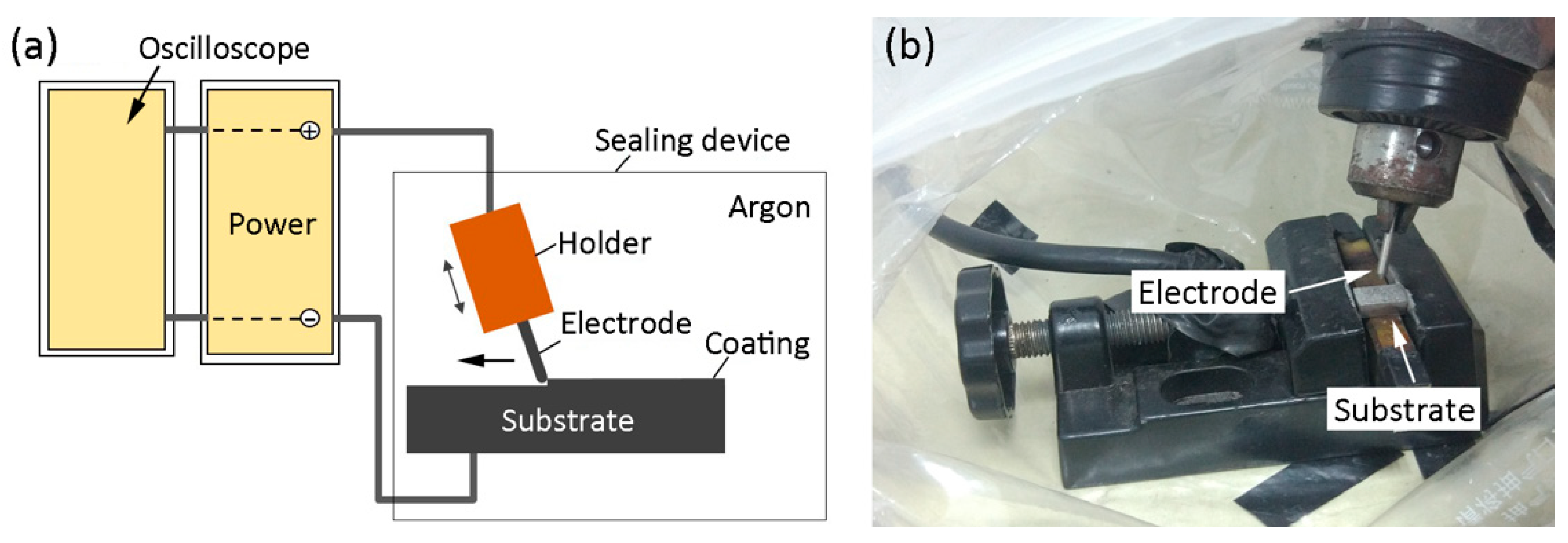
The experiments were carried out with a 3H-ES-6G type ESD equipment (Institute of Metal Research, Shenyang, China). The deposition was performed with the output voltage of 40–80 V and the pulse repetition frequency of 50–500 Hz. A new type Ar-rich sealed protective system, in which the residual oxygen concentration was in the range of 0.04–0.06%, was used for protecting the deposit zone. The rotate speed of the electrode was about 600 r/min. The schematic diagram of the ESD system and the experimental setup are shown in Figure 1.
2.2. Microstructural Characterization and Microhardness
After deposition, the specimens were cut from transverse cross-sections of the deposited coating. Metallographic samples were mounted, polished, and etched by 0.5% HF in line with standard procedures. The scanning electron microscope (SEM, Tescan, Brno, Czech Republic) were employed to characterize and investigate the cross-sectional morphology and microstructure of the coating. The phase composition of the deposited coating was analyzed by the X’Pert Pro type X-ray diffraction (XRD, PNAlytical, Alemlo, The Netherlands) with accelerating voltage of 40 kV, beam current of 40 mA, 2θ-angle scan range of 30°–90°, angular scanning step of 0.05° and counting time per step of 0.8 s. The microhardness was measured with a HX-1000 type micro-hardness tester (Shanghai Optical Instrument Factory, Shanghai, China) under the applied load of 50 g and the load time of 15 s.
2.3. Simulation
2.3.1. Governing Equation
For the transient, non-linear thermal analysis of single ESD process, discharge spark channels were considered to be cylindrical column. According to the heat transfer theory, a Fourier heat conduction equation was taken as the governing equation [16]:
where ρ is the density, kg·m−3; cp is the specific heat, J·kg−1·°C−1; T is the temperature, °C; t is the time, s; λ is the thermal conductivity, W·m−1·°C−1; and r and z are the coordinates of cylindrical work domain, respectively.
2.3.2. Initial Conditions and Boundary Conditions
Gaussian heat flux, which is a function of discharge time and radial distance, was used to simulate the heat flow of a single discharge. The Gaussian heat flux is shown in Equation (2) [16]:
where H(r,t) is heat flux, r is the radial distance from the plasma center, t is the discharge time, U is discharge voltage, I is discharge current and k is the fraction of plasma energy to the substrate, which was chosen as 45%. Shape coefficient of Gaussian curve (m) was set to 0.5. R(t) was the time-dependent plasma radius [17].
In the heat transfer analysis, the initial temperature of the entire model was assumed to be consistent with the environment temperature (T0 = 20 °C). The boundary conditions on the top surface were divided into two cases:
when 0 ≤ r ≤ R(t),
and when r ≥ R(t),
where hc is the coefficient of heat convection and was set to 100 W·m−2·°C−1.
The other three sides of the surfaces of the model were thermostatic surfaces, thus the discharge point was small and the area was far from the discharge point.
2.3.3. Finite Element Model and Material Properties
The ABAQUS/standard was chosen for simulating the temperature variation of single thin deposited layer during deposition process. Figure 2a,b shows the meshes of the model, which consisted of four-node finite elements. Two typical thin deposited layers based on actual samples, namely Type I (Figure 2a) and Type II (Figure 2b), were considered. The dimension of the model was determined by half of the true size of the specimens, and the simulation conditions were chosen based on the studies of actual deposition experiments.
A few assumptions were made for the simulation:
- Heat flux of individual electrical discharge had a Gaussian distribution, which was a function of time and space.
- In the heat transfer analysis, heat conduction and convection were considered, while radiation was ignored.
- Material properties were homogeneous on temperature.
Table 1 lists the physical properties of Ti6Al4V alloy with temperature change.
2.4. Evaluation of Wear Resistance
Sliding wear tests of the ESD coating were carried out on a Cetr-UMT-3 Multi-Specimen Test System (Center for Tribology, Campbell, CA, USA) at room temperature in air. A ball of GCr15 (6 mm in diameter) was used as the counter pair. The coating specimens were allowed with a sliding speed of 40 mm/s under a load of 5 N, and the test time was 20 min. The wear rate was calculated by the following formula:
where W is the wear rate, cm2•N−1; M is the wear loss, mg; ρ is the density, g·cm−3; F is the contact force, N; and L is the wear track, cm. The electronic analytical balance (0.1 mg) was used to measure the mass loss.
3. Results and Discussion
3.1. Cross-Sectional Morphology
The typical cross-sectional morphology of the deposited coating is shown in Figure 3. Figure 3a shows that the average thickness of the coating along the cross section is over 550 µm. The interface between the deposited coating and the substrate is even and flawless (Figure 3b), which indicates that a good metallurgical bond was obtained. In fact, the main formation mechanism of ESD coating is drop transfer. In deposition, the discharge periodically generates between the electrode and the substrate and heats the adjoining zones of both the electrode and the substrate over melting point expeditiously. At the same time, the molten material falls from the electrode, move towards the substrate and finally spread onto the substrate surface to form thin deposited layer [11], which is diagrammatically displayed in Figure 4. The thick deposited coatings shown in Figure 3a are constituted of many thin deposited layers above. In solidification of each drop transfer, the droplet and the thin molten pool on the substrate surface fuse into one thin deposited layer, which is the reason the good metallurgical bond was obtained (Figure 3b).
A further observation on the cross-section with high magnification is shown in Figure 5. It can be observed that there are some defects, such as voids and inclusions, in the coating. The formation of voids and inclusions can be mainly attributed to the rapid cooling characteristics of ESD process. High cooling rate results in high solidification rate, which sometimes lead to the appearance of incomplete fusion between different thin deposited layers. In addition, the formation of voids is also related to the mixing and generation of gases in deposition [18].
3.2. Microstructure
Figure 6 shows the typical microstructure of the deposited coating displayed in Figure 3a. The deposited coating is mainly composed of acicular phases. The crystallographic structures were analyzed using X-ray diffraction (XRD) with 2θ range from 30° to 90°. Figure 7 shows the XRD patterns of the deposited coating that can be indexed as close-packed hexagonal structure according to the relevant PDF card. In electro-spark deposition, the deposited material undergoes rapid melt and subsequent ultra-rapid solidification, which might cause the formation of close-packed hexagonal martensite.
In solidification, the degree of martensite transformation is related to the cooling rate below β transus temperature. A cooling rate of thin deposited layers above 410 °C/s will allow the formation of a completely martensitic structure, while a cooling rate below 410 °C/s will result in mixed microstructures of martensitic α’, massive α and various diffusion controlled α [19]. Figure 8a shows the temperature evolution of Points A and B shown in Figure 2. The temperature profiles show rapid rise and fall characteristics, which correspond to the rapid heating and cooling phenomena in ESD process. The cooling rate is shown in Figure 8b. For both Type I and Type II thin deposited layers shown in Figure 2, the cooling rate is always above the critical cooling rate of β to α’ phase transformation (410 °C/s), which results in the formation of a large amount of α’ martensite. The crystal structure variation of this transformation from body centered cubic (bcc) to close-packed hexagonal (hcp) is shown in Figure 9. In addition, the diffraction peak broadening displayed in Figure 7, which can be attributed to the diffuse scattering of the microcrystal, also confirms the presence of α’ martensite in the coating [20,21].
3.3. Microhardness
The microhardness was tested on the cross section of the specimen after ESD treatment. The distribution curve is shown in Figure 10. It can be seen that the hardness distribution of the deposited coating is uneven. The average hardness of the coating is about 540 HV0.05, which is higher than that of the substrate (about 330 HV0.05). The increase on hardness of the deposited coating partially relates to the characteristics of ESD technology and the structural changes. Firstly, electro-spark deposition provides a high solidification rate, which results in the increase of nucleation rate and microstructure refine. Secondly, the formation of metastable structure during rapid solidification can improve the solid solution strengthening effect. Therefore, rapid cooling and subsequent martensitic transformation can improve the performance of many titanium alloys [22].
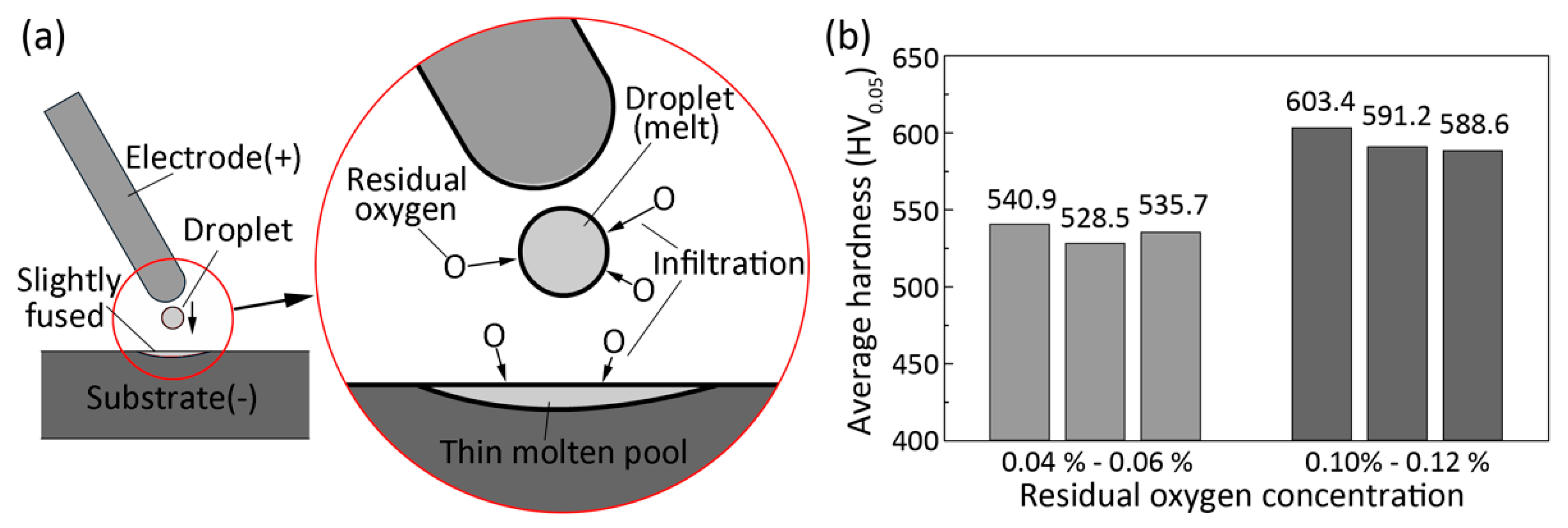
However, because of the small lattice distortion of acicular martensitic α’ structure in titanium alloy, the strengthening effect is slight [23]. The solid solution of oxygen in deposited coating is also a conceivable origin for hardness improving. In deposition process, the droplets and the thin molten pool are both in the liquid state and exposed to the shielding atmosphere, which is diagrammatically illustrated in Figure 11a. According to the Ti-O phase diagram [24], the oxygen can easily dissolve into the liquid Ti under high temperature. During the following rapid solidification, the dissolved oxygen cannot escape sufficiently and will exist in the solidified thin deposited layers. Additionally, the fact that the oxygen can be absorbed intensely by high temperature (>600 °C) titanium alloy has been widely reported in the past few decades. In experiment, the measured value of residual oxygen concentration in shielding atmosphere is 0.04–0.06%. This concentration of residual oxygen in shielding atmosphere is insufficient to form massive metal oxide, which has been substantiated in the XRD results shown in Figure 7. As a candidate, the solid solution became the main existing form because the solubility of oxygen in solid titanium is higher than 10 wt. % under high temperature (>800 °C) [24]. As is well known, the solid solution of oxygen can dramatically harden the matrix phase of titanium alloys [25]. In titanium, the lattice parameters of the hexagonal close packed crystal structure are a = 0.295 nm and c = 0.468 nm, giving a c/a ratio of 1.587. For an ideally close packed hexagonal lattice, the c/a ratio is 1.633. Compared to the ideally packed hexagonal crystal structure, the reduced c/a ratio leads to a larger spacing between prism planes, which is beneficial to plastic deformation. However, the insertion of interstitially dissolved atom O in the hcp lattice slightly increases the c/a ratio. As a result, the plastic deformation becomes difficult and the hardness increases.
To verify the hypothesis above, contrast tests with different residual oxygen concentration in shielding atmosphere (other parameters and conditions are same) were performed. The results are shown in Figure 11b. For each residual oxygen concentration, three parallel samples were tested and the average hardness was adopted to make the results reliable. It is evident that high concentration of residual oxygen results in high hardness. These results indicate that the oxygen plays an important role in the hardening of deposited coating.
In fact, existing research results have indicated that the strengthening effect of martensitic transformation in Ti6Al4V alloy is not intense and the hardness is usually not more than 450 HV. These results above imply that the solution of oxygen from the argon-rich atmosphere to the micro molten pool is another conceivable reason for explaining why the deposited coating is hardened.
3.4. Wear Resistance
The variations of the mass loss with test time for the deposited coating and the substrate are shown in Figure 12a. The cumulative mass loss of the deposited coating specimen was about 1.58 mg, while the mass loss of the substrate specimen was about 3.6 mg. For convenience, the mass loss has been translated to the wear rate, which is also shown in Figure 12a with a special coordinate axis on the right part. The wear rate of the deposited coating is about 2.23 times higher than that of the substrate, which implies that the deposited coatings possess better wear resistance than Ti6Al4V substrate.
According to the Archard theory, the wear loss M of specimens is calculated as [26,27]:
where F is the contact force (N), x is the wear track (mm), H is the hardness (HV) and k is the dimensionless wear coefficient. Therefore, the wear loss is proportional to the contact force and the wear track, and is inversely proportional to the surface hardness of the specimens.
The curves of friction coefficients are shown in Figure 12b. At the first stage of wear test, the friction coefficients of both the deposited coating and the substrate quickly increased to create a trace on the surface. After the trace occurred on the surface, the average friction coefficients of the deposited coating specimen and the substrate specimen gradually stabilized at 0.76 and 0.57, respectively. The friction coefficient of the deposited coating is permanently less than that of the Ti6Al4V substrate. In addition, the fluctuation range of deposited coating is relatively small, which implies that the deposited coating has a relatively stable friction resistance. On the contrary, the fluctuation range of the friction coefficient of substrate specimen is large.
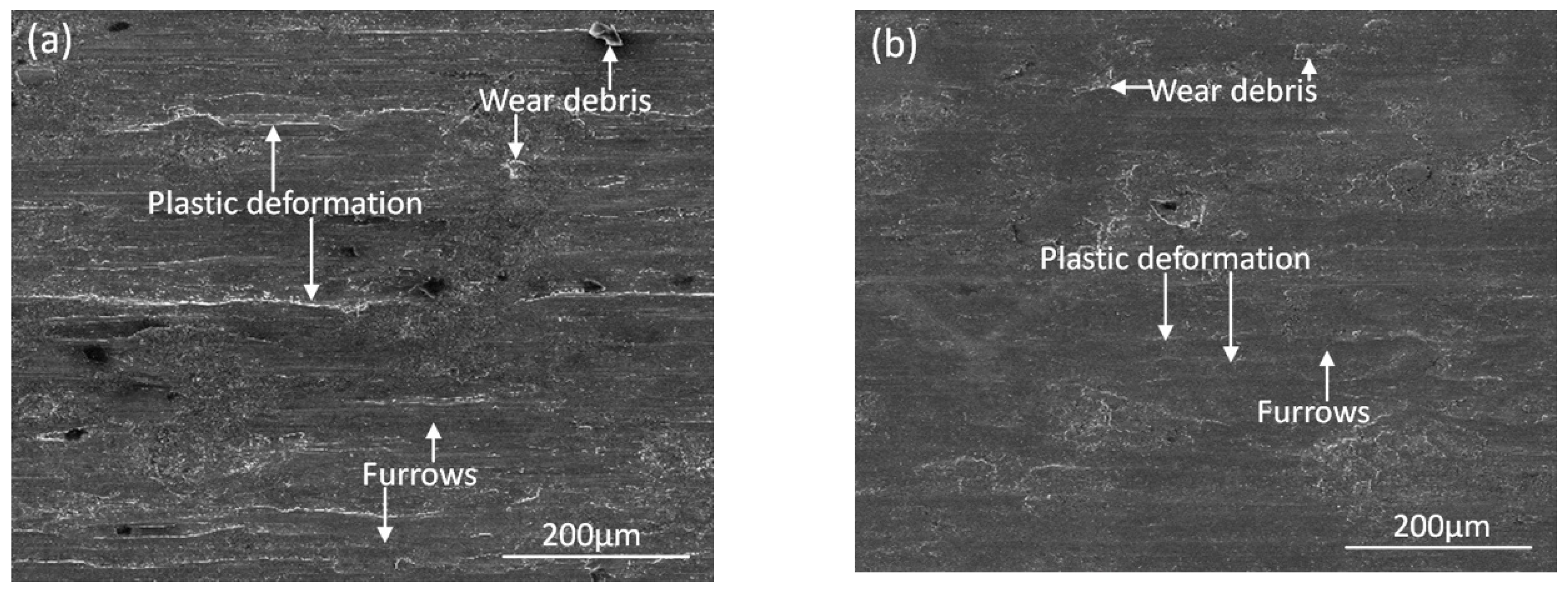
Figure 13 shows the worn surface of the substrate and the deposited coating specimens. As displayed in Figure 13a, furrows and wear debris on the wear track of the substrate specimen could be observed. This morphology displays typical characteristics of micro-cutting and adhesive wear. In sliding wear process, the load is transmitted to the worn surface normally and tangentially by contact point, and shear stress and normal stress generate on the micro-embossment of the substrate surface. Due to the reciprocating effect of the load, the micro-embossment of the surface can produce plastic deformation and fracture under the action of shear stress, forming wear debris. At the same time, the normal stress transmitted along the normal direction causes scratches and groove on the surface of the substrate. The metal on both sides of the groove undergo plastic deformation and accumulation. In the subsequent wear process, the accumulated debris is flattened again and eventually leads to micro-cutting and adhesion wear.
The worn surface of the deposited coating specimen is shown in Figure 13b. The plastic deformation, furrow and wear debris indicate that the wear mechanism of the deposited coating is similar to the substrate. Compared with the substrate specimen, the friction traces of the coating surface are relatively shallow, which implies that the deposited coating possess better wear resistance. The enhancement on hardness of the deposited coating is the main reason for the improvement of wear resistance for that better deformation resistance was obtained. In addition, the improvement on wear resistance of the deposited coating can also be partially attributed to the grain refinement and the martensite transformation, which mildly improved the deformation resistance of the coating further. As a comparison, adhesion wear is prone to occur on the substrate specimen surface under the same conditions due to the low hardness, which is the conceivable reason for the phenomenon that the wear of substrate is relatively serious and the fluctuation of the friction coefficient is acute.
4. Conclusions
In this present work, electro-spark deposition was applied to the fabrication of Ti6Al4V deposited coatings. The microstructure, phase composition, microhardness and wear resistance of these deposited coatings were investigated. The following main conclusions can be drawn:
- (1)
- The Ti6Al4V coating with a thickness of more than 550 µm was successfully prepared by electro-spark deposition. The interface between the deposited coating and the underlying substrate is even and consecutive, which implies that a good metallurgical bond was obtained.
- (2)
- The deposited coating is mainly composed of α’ martensite. The average hardness of the ESD coating is 540 HV which is about 1.6 times that of the substrate.
- (3)
- The deposited coating shows better wear resistance, thus the cumulative mass loss was less than that of the substrate and the friction coefficient decreased by 0.19. The enhancement on hardness of the deposited coatings is the main reason for this improvement of wear resistance.
Author Contributions
Conceptualization, W.W.; Methodology, W.W.; Software, C.H.; Validation, W.W. and C.H.; Formal analysis, C.H.; Investigation, W.W.; Writing—Original Draft Preparation, W.W. and C.H.; Writing—Review and Editing, W.W. and C.H.; Supervision, W.W.; and Funding Acquisition, W.W.
Funding
This work was supported by the Natural Science Foundation of Zhejiang Province (LY14E050008).
Conflicts of Interest
The authors declare no conflict of interest.
References
- Makama, Z.; Doble, I.; Nicolson, D.; Webb, M.E.; Beech, I.B.; Campbell, S.A.; Smith, J.R. Surface preparation of stainless steel 316L, bronze CW451K and titanium Ti6Al4V for bonding to polyurethane in marine cable connector assemblies. Trans. Inst. Met. Finish. 2011, 89, 237–243. [Google Scholar] [CrossRef]
- Balasubramanian, M.; Jayabalan, V.; Balasubramanian, V. A mathematical model to predict impact toughness of pulsed-current gas tungsten arc-welded titanium alloy. Int. J. Adv. Manuf. Technol. 2008, 35, 852–858. [Google Scholar] [CrossRef]
- Cvijović-Alagić, I.; Gubeljak, N.; Rakin, M.; Cvijović, Z.; Gerić, K. Microstructural morphology effects on fracture resistance and crack tip strain distribution in Ti–6Al–4V alloy for orthopedic implants. Mater. Des. 2014, 53, 870–880. [Google Scholar] [CrossRef]
- Ceschini, L.; Lanzoni, E.; Martini, C.; Prandstraller, D.; Sambogna, G. Comparison of dry sliding friction and wear of Ti6Al4V alloy treated by plasma electrolytic oxidation and PVD coating. Wear 2008, 264, 86–95. [Google Scholar] [CrossRef]
- Lütjering, G. Influence of processing on microstructure and mechanical properties of (α+β) titanium alloys. Mater. Sci. Eng. A 1998, 243, 32–45. [Google Scholar] [CrossRef]
- Yetim, A.F.; Celik, A.; Alsaran, A. Improving tribological properties of Ti6Al4V alloy with duplex surface treatment. Surf. Coat. Technol. 2010, 205, 320–324. [Google Scholar] [CrossRef]
- Liu, Y.; Wang, D.P.; Deng, C.Y.; Huo, L.X.; Wang, L.J.; Cao, S. Feasibility study on preparation of coatings on Ti–6Al–4V by combined ultrasonic impact treatment and electrospark deposition. Mater. Des. 2014, 63, 488–492. [Google Scholar] [CrossRef]
- Obadele, B.A.; Andrews, A.; Olubambi, P.A.; Mathew, M.T.; Pityana, S. Effect ofZrO2 addition onthedryslidingwearbehavioroflaserclad Ti6Al4V alloy. Wear 2015, 328–329, 295–300. [Google Scholar] [CrossRef]
- Korkmaz, K. Investigation and characterization of electrospark deposited chromium carbide-based coating on the steel. Surf. Coat. Technol. 2015, 272, 1–7. [Google Scholar] [CrossRef]
- Çakir, A.; Yilmaz, M.S.; Ribalko, A.; Korkmaz, K. A Study on modification of micro-alloy steel surfaces with different hard materials via electro-spark deposition method. Acta Phys. Polonica A 2015, 127, 1410–1413. [Google Scholar] [CrossRef]
- Reynolds, J.L.; Holdren, R.L.; Brown, L.E. Electro-spark deposition. Adv. Mater. Process. 2003, 161, 35–37. [Google Scholar]
- Li, Z.W.; Gao, W.; Yoshihara, M.; He, Y.D. Improving oxidation resistance of Ti3Al and TiAl intermetallic compounds with electro-spark deposit coatings. Mater. Sci. Eng. A 2003, 347, 243–252. [Google Scholar] [CrossRef]
- Tang, J.M. Mechanical and tribological properties of the TiC–TiB2compositecoating deposited on 40Cr-steel by electro spark deposition. Appl. Surf. Sci. 2016, 365, 202–208. [Google Scholar] [CrossRef]
- Wei, X.; Chen, Z.G.; Zhong, J.; Wang, L.; Hou, Z.W.; Zhang, Y.; Tan, F.L. Facile preparation of nanocrystalline Fe2B coating by direct electrospark deposition of coarse-grained Fe2B electrode material. J. Alloys Compd. 2017, 717, 31–40. [Google Scholar] [CrossRef]
- Liu, D.Y.; Gao, W.; Li, Z.W.; Zhang, H.F.; Hu, Z.Q. Electro-spark deposition of Fe-based amorphous alloy coatings. Mater. Lett. 2007, 61, 165–167. [Google Scholar] [CrossRef]
- Patel, M.R.; Barrufet, M.A.; Eubank, P.T.; DiBitonto, D.D. Theoretical models of the electrical discharge machining process. II. The anode erosion model. J. Appl. Phys. 1989, 66, 4104–4111. [Google Scholar] [CrossRef]
- Liu, J.F.; Guo, Y.B. Thermal modeling of EDM with progression of massive random electrical discharges. Procedia Manuf. 2016, 5, 495–507. [Google Scholar] [CrossRef]
- Lee, H.T.; Tai, T.Y. Relationship between EDM parameters and surface crack formation. J. Mater. Process. Technol. 2003, 142, 676–683. [Google Scholar] [CrossRef]
- Ahmed, T.; Rack, H.J. Phase transformations during cooling in α+β titanium alloys. Mater. Sci. Eng. A 1998, 243, 206–211. [Google Scholar] [CrossRef]
- Xie, Y.J.; Wang, M.C. Epitaxial MCrAlY coating on a Ni-base superalloy produced by electrospark deposition. Surf. Coat. Technol. 2006, 201, 3564–3570. [Google Scholar] [CrossRef]
- Jain, P.; Mandal, T.; Prakash, P.; Garg, A.; Balani, K. Electrophoretic deposition of nanocrystalline hydroxyapatite on Ti6Al4V/TiO2 substrate. J. Coat. Technol. Res. 2013, 10, 263–275. [Google Scholar] [CrossRef]
- Sundaresan, S.; Ram, G.D.J. Use of magnetic arc oscillation for grain refinement of gas tungsten arc welds in α–β titanium alloys. Sci. Technol. Weld. Join. 2013, 4, 151–160. [Google Scholar] [CrossRef]
- Huang, Z.Y.; Guo, Z.J.; Wen, G.P.; Li, Q. Mechanical properties of TC4 alloy annealed with different processes. Heat Treat. Met. 2015, 40, 175–179. (In Chinese) [Google Scholar] [CrossRef]
- Tang, R.Z.; Tian, R.Z. Binary Alloy Phase Diagrams and Crystal Structure of IntermediadePhase, 1st ed.; Central South University Press: Changsha, China, 2009; p. 909. (In Chinese) [Google Scholar]
- Na, T.W.; Kim, W.R.; Yang, S.M.; Kwon, O.; Park, J.M.; Kim, G.H.; Jung, K.H.; Lee, C.W.; Park, H.K.; Kim, H.G. Effect of laser power on oxygen and nitrogen concentration of commercially pure titanium manufactured by selective laser melting. Mater. Charact. 2018, 143, 110–117. [Google Scholar] [CrossRef]
- Archard, J.F. Contact and rubbing of flat surfaces. J. Appl. Phys. 1953, 24, 981–988. [Google Scholar] [CrossRef]
- Archard, J.F.; Hirst, W. The wear of metals under unlubricated conditions. Proc. R. Soc. Lond. A 1956, 236, 397–410. [Google Scholar] [CrossRef]
Figure 1.
Schematic diagram of electro-spark deposition system (a); and the experimental setup (b).

Figure 2.
FEM mesh of the model: (a) typical thin deposited Layer I (Type I); and(b) typical thin deposited Layer II (Type II).
Figure 2.
FEM mesh of the model: (a) typical thin deposited Layer I (Type I); and(b) typical thin deposited Layer II (Type II).
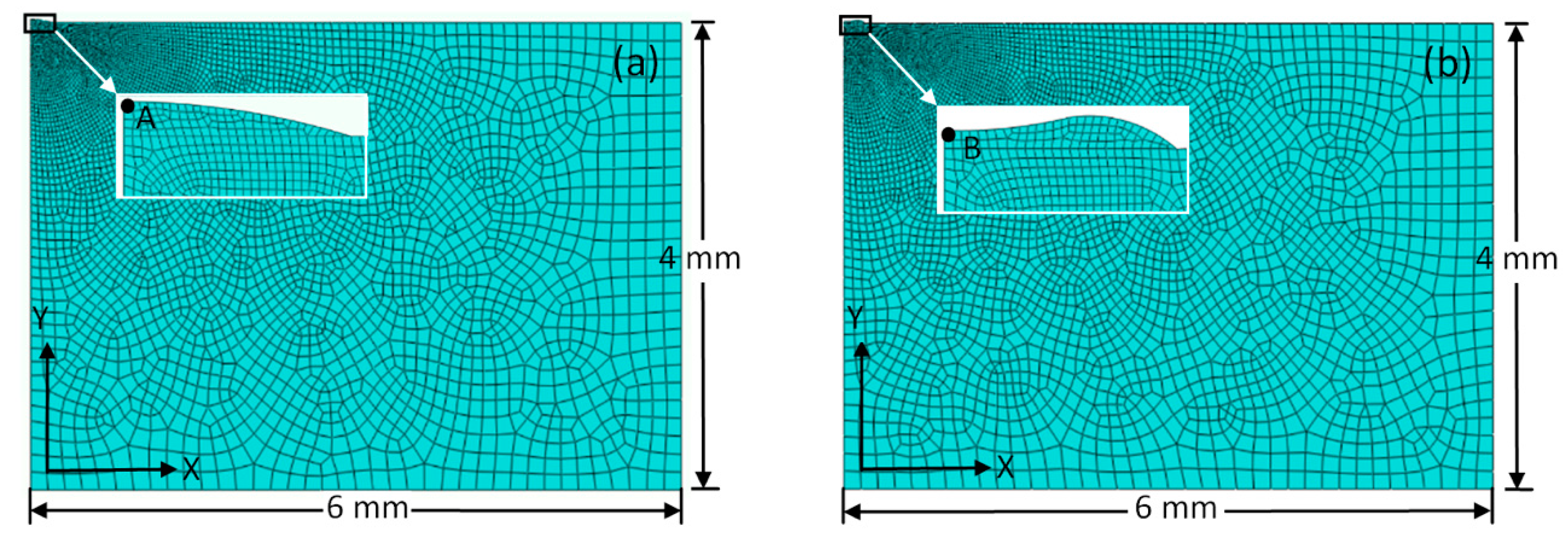
Figure 3.
Cross-sectional morphology of the Ti6Al4V deposited coating: (a) general view; and (b) the interface.
Figure 3.
Cross-sectional morphology of the Ti6Al4V deposited coating: (a) general view; and (b) the interface.
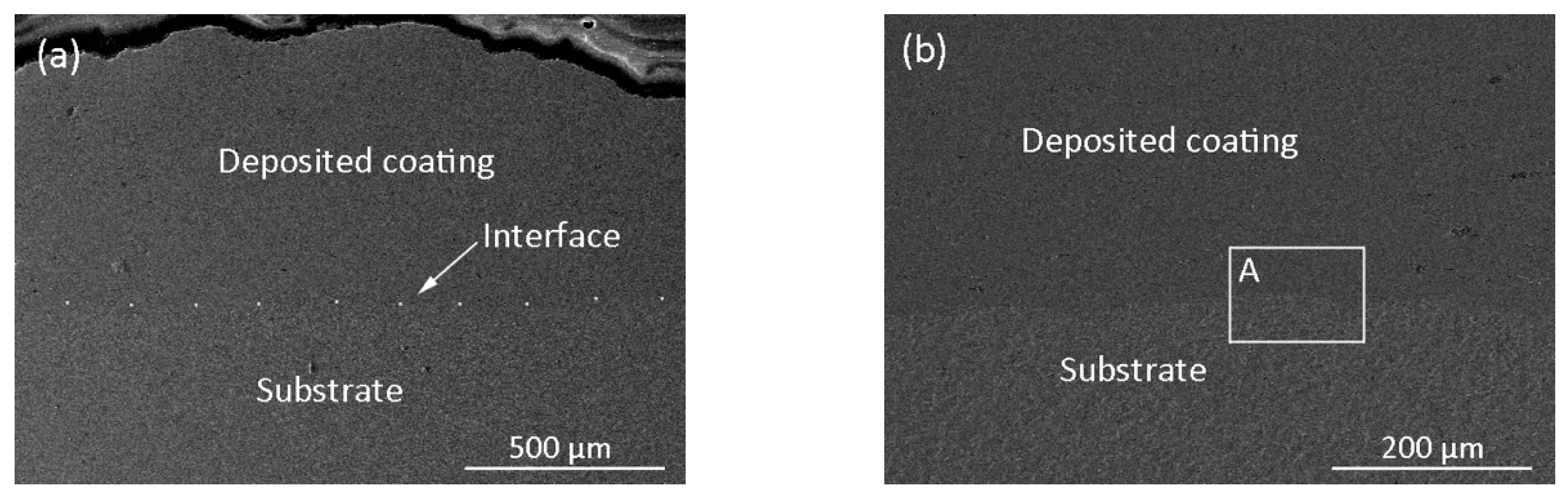
Figure 4.
Droplet transition process.
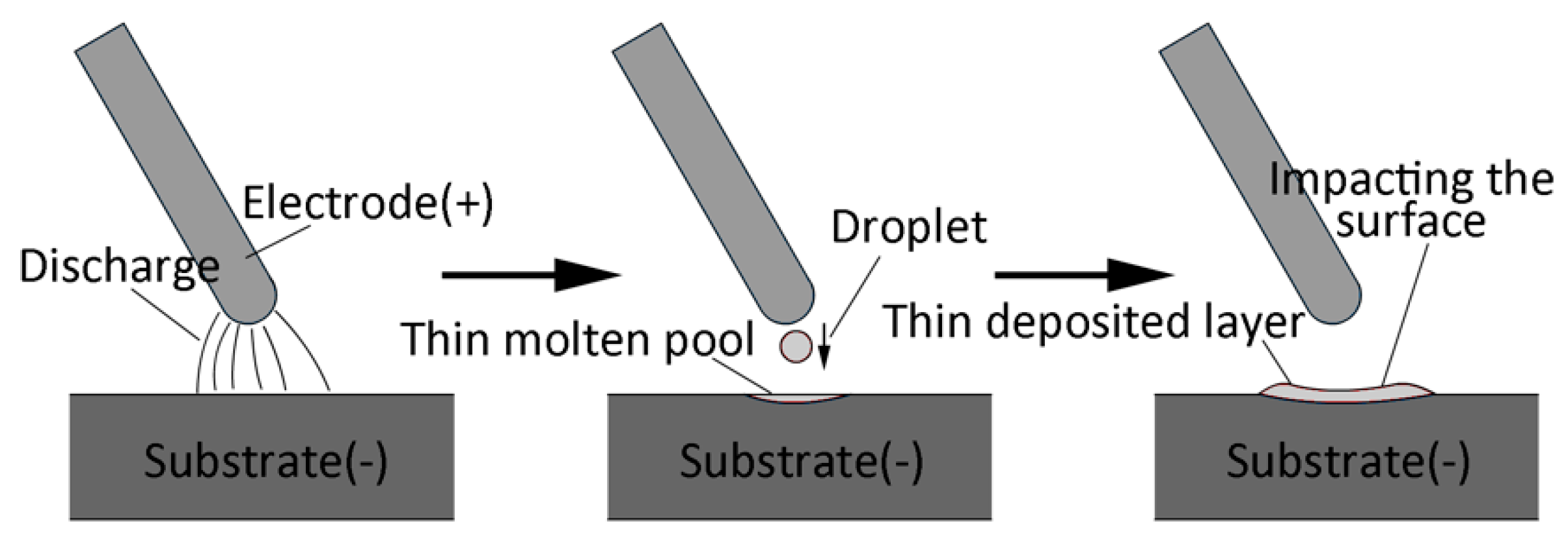
Figure 5.
Magnification of marked region “A” in Figure 2b.
Figure 5.
Magnification of marked region “A” in Figure 2b.
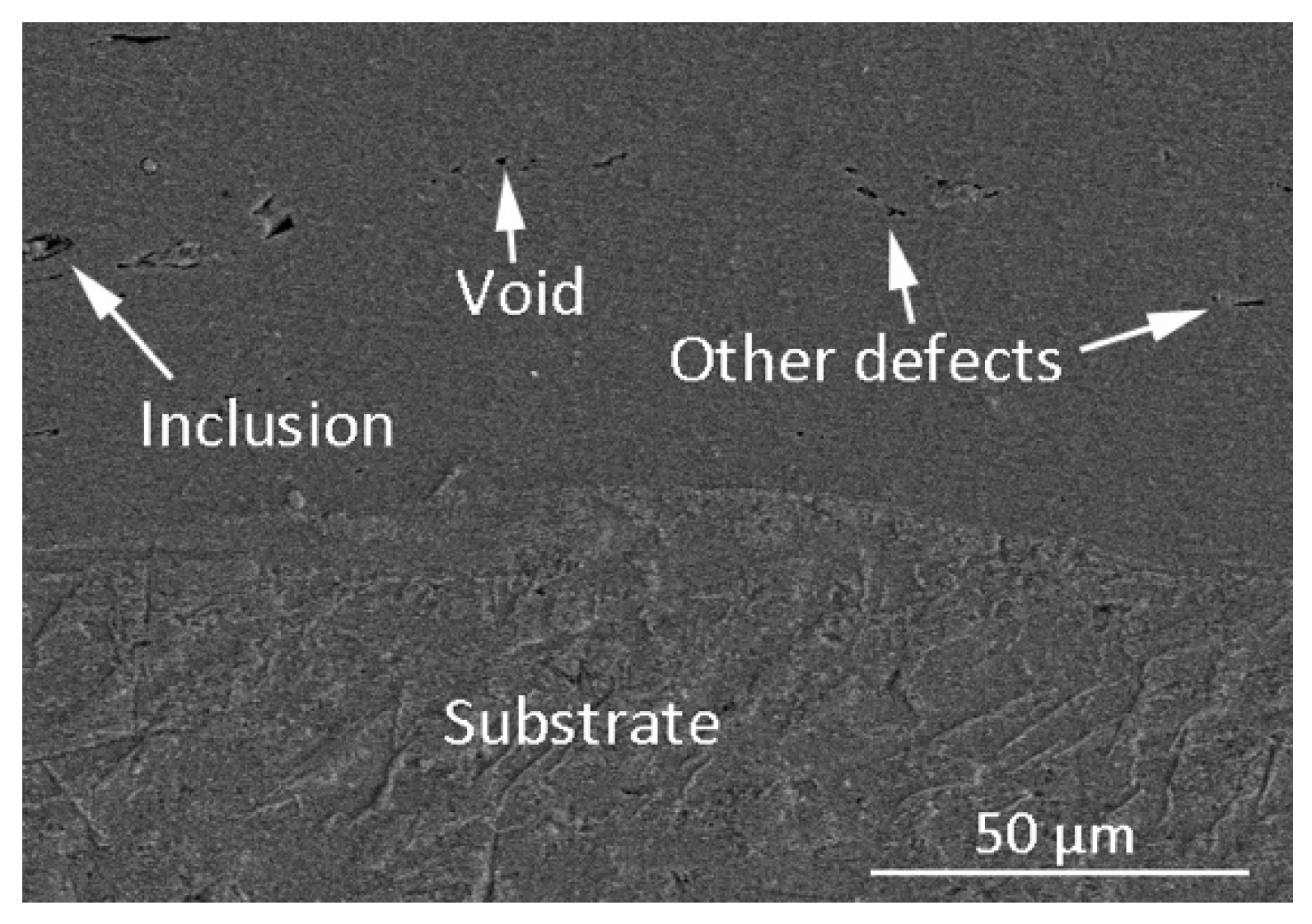
Figure 6.
Microstructure of the Ti6Al4V deposited coating.
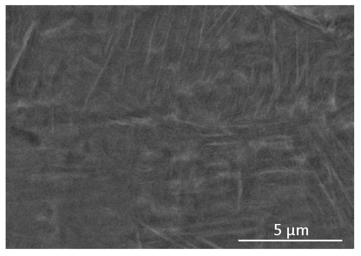
Figure 7.
XRD pattern of Ti6Al4V deposited coating.
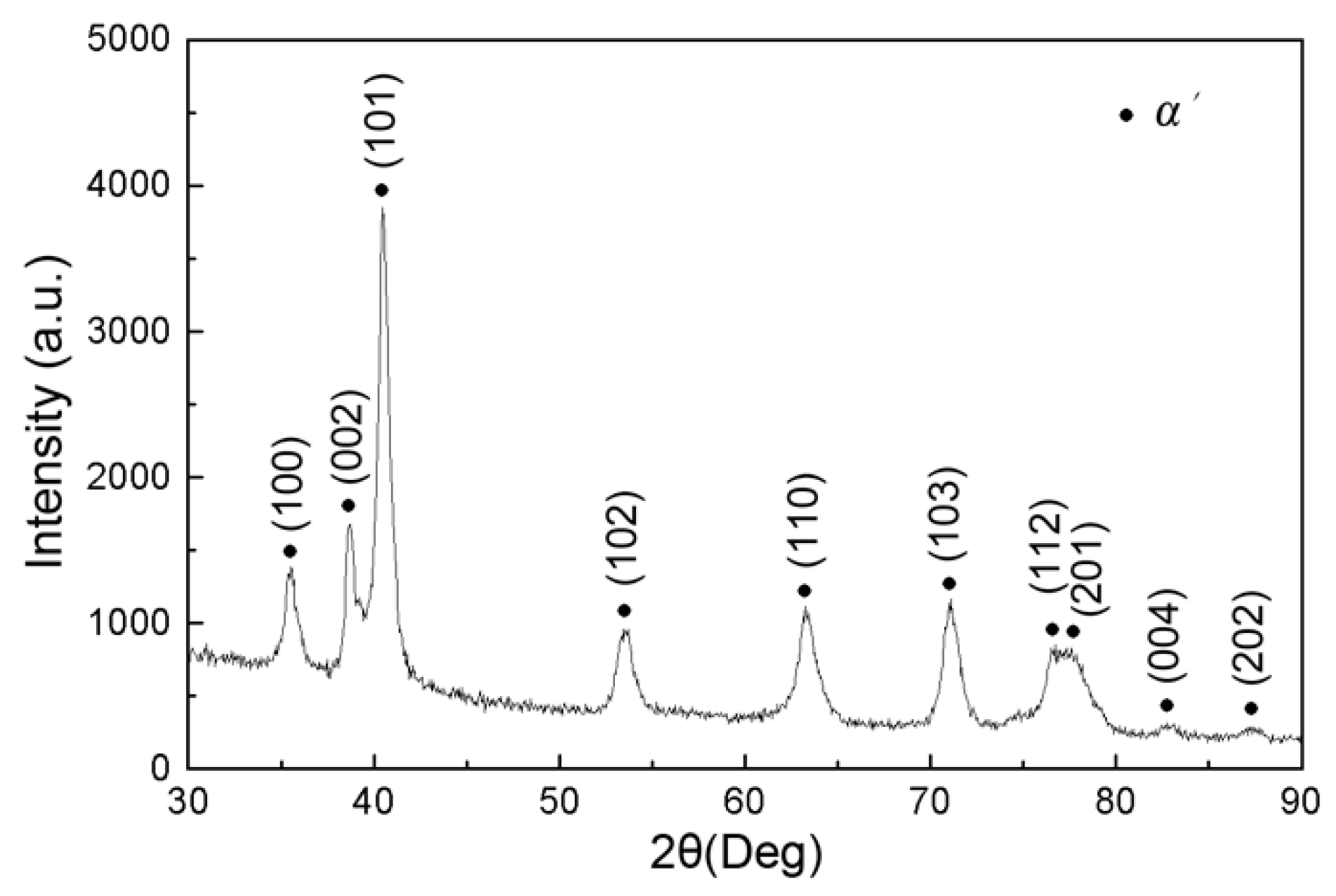
Figure 8.
Temperature evolution (a); and cooling rate (b) of Points A and B shown in Figure 2.
Figure 8.
Temperature evolution (a); and cooling rate (b) of Points A and B shown in Figure 2.
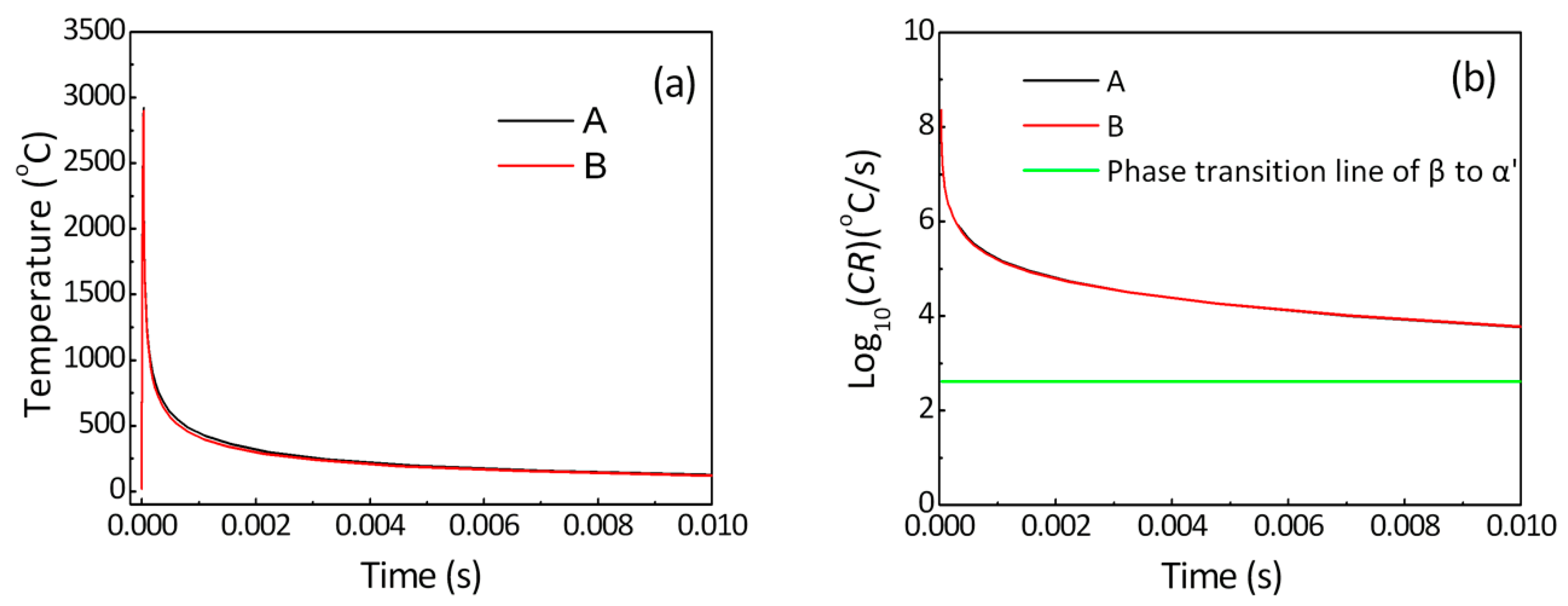
Figure 9.
Crystal structure variation of martensite transformation (from bcc to hcp).
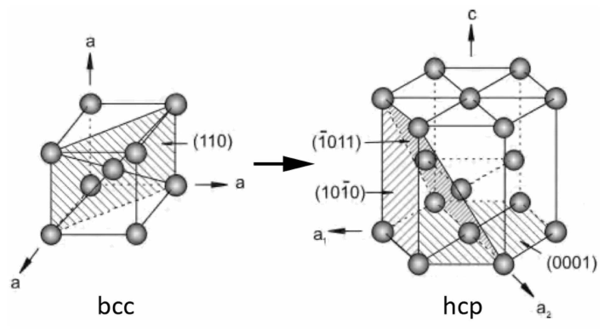
Figure 10.
Microhardness distribution along the depth direction.
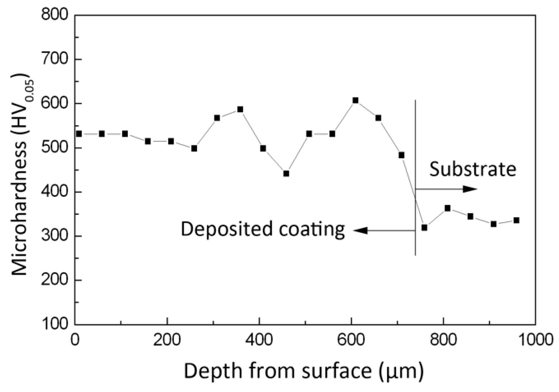
Figure 11.
The infiltration of residual oxygen in deposition process (a); and the results of contrast testswith different residual oxygen concentration in shielding atmosphere (b).
Figure 11.
The infiltration of residual oxygen in deposition process (a); and the results of contrast testswith different residual oxygen concentration in shielding atmosphere (b).

Figure 12.
The comparison of wear test for deposited coating and substrate: (a) mass losses; and (b) friction coefficients.
Figure 12.
The comparison of wear test for deposited coating and substrate: (a) mass losses; and (b) friction coefficients.
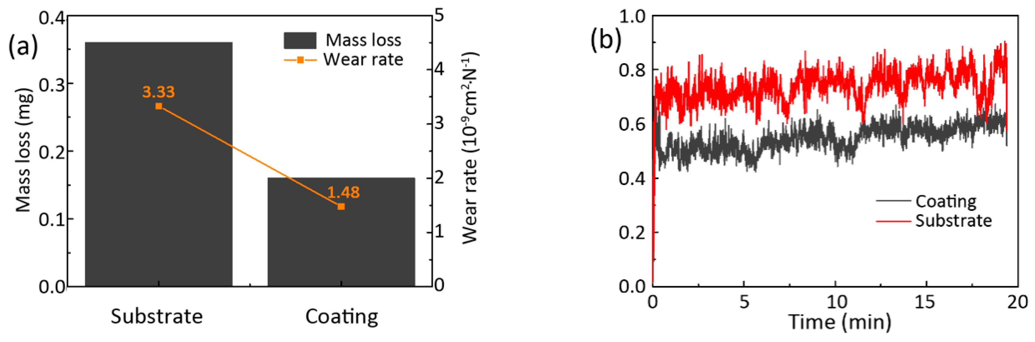
Figure 13.
The typical micrograph of the worn surface: (a) substrate specimen; and (b) deposited coating specimen.
Figure 13.
The typical micrograph of the worn surface: (a) substrate specimen; and (b) deposited coating specimen.

Table 1.
Physical properties of Ti6Al4V alloy.
| Temperature (°C) | Density (Kg/m3) | Coefficient of Thermal Expansion (per °C) | Thermal Conductivity (W/m °C) | Specific Heat (J/kg °C) |
|---|---|---|---|---|
| 20 | 4500 | 8.6 × 10⁻⁶ | 7.95 | 611 |
| 500 | 4410 | 9.7 × 10⁻⁶ | 11.8 | 703 |
| 1000 | 4350 | 10.2 × 10⁻⁶ | 15.5 | 1030 |
| 1500 | 4330 | 10.6 × 10⁻⁶ | 21.1 | 1850 |
| 2000 | 4300 | 11.1 × 10⁻⁶ | 22.7 | 1852 |
© 2018 by the authors. Licensee MDPI, Basel, Switzerland. This article is an open access article distributed under the terms and conditions of the Creative Commons Attribution (CC BY) license (http://creativecommons.org/licenses/by/4.0/).
Share and Cite
MDPI and ACS Style
Wang, W.; Han, C. Microstructure and Wear Resistance of Ti6Al4V Coating Fabricated by Electro-Spark Deposition. Metals 2019, 9, 23. https://doi.org/10.3390/met9010023
AMA Style
Wang W, Han C. Microstructure and Wear Resistance of Ti6Al4V Coating Fabricated by Electro-Spark Deposition. Metals. 2019; 9(1):23. https://doi.org/10.3390/met9010023
Chicago/Turabian StyleWang, Weifu, and Chao Han. 2019. "Microstructure and Wear Resistance of Ti6Al4V Coating Fabricated by Electro-Spark Deposition" Metals 9, no. 1: 23. https://doi.org/10.3390/met9010023
Note that from the first issue of 2016, this journal uses article numbers instead of page numbers. See further details here.