Preparing and Mounting Polymer Nanofibers onto Microscale Test Platforms


Mechanical Engineering Department, Carnegie Mellon University, Pittsburgh, PA 15217, USA
*
Author to whom correspondence should be addressed.
Actuators 2018, 7(4), 71; https://doi.org/10.3390/act7040071
Submission received: 7 September 2018
/
Revised: 10 October 2018
/
Accepted: 10 October 2018
/
Published: 15 October 2018
(This article belongs to the Special Issue Micromanipulation)
Abstract
:Because they can achieve a high degree of molecular chain alignment in comparison with their bulk counterparts, the mechanical and thermal properties of polymer nanofibers are of great interest. However, due to their nanometer-scale size, it is difficult to manipulate, grip, and test these fibers. Here, we demonstrate simple repeatable methods to transfer as-drawn fibers to micrometer-scale test platforms where their properties can be directly measured. Issues encountered and methods to minimize measurement artifacts are also discussed.

1. Introduction
Polymer nanofibers have mechanical and thermal properties significantly higher than their bulk counterparts [1,2,3,4,5,6]. They have a wide range of potential applications in areas such as tissue engineering, sensing, reinforcing composites, ballistic armor, textiles, and in improving thermal management [7,8,9,10,11]. Detailed study of their material properties is necessary to assess their true application possibilities.
However, due to their nanometer-scale size, it is difficult to manipulate and mount individual polymer nanofibers onto a test platform to make measurements. The macroscale approach of manipulating objects with pick-and-place tools has been scaled to smaller sizes using micro- and nanoscale grippers [12,13,14]. A tweezer-like gripping mechanism in these grippers can be obtained using various actuation mechanisms such as electrostatic, thermal, shape memory, fluidic, magnetic, and piezoelectric [14]. But it is difficult to ensure reliable placement of a long nanofiber onto a horizontal platform using a nanogripper. Optical tweezing is capable of sorting and manipulating an individual DNA molecule. This technique requires a liquid medium, which is not compatible with mechanical measurement platforms operating in laboratory air [15]. Another common approach is to use an atomic force microscope (AFM) cantilever tip or a tungsten tip mounted on a precision XYZ manipulator. This has been successfully used for nanoscale fabrication of polymer nanofibers [16] and precision mounting of nanofibers [1,17]. This approach is low yield and time-consuming. In addition, the process is generally performed in a scanning electron microscope (SEM) [17] because nanofibers are difficult to resolve optically. However, polymer nanofibers are damaged by electron-beam irradiation [18]. Hence, reliable optical methods are strongly needed for manipulation and testing.
In view of the urgent need for such micromanipulation, this article describes and demonstrates a simple specimen collector technique that enables nanofiber placement with ±1 µm precision onto micromachined test platforms using optical methods. Electrospinning is one common method to make such long fibers [9,19,20]. Here, as an alternative example, we describe a method by which ultra-high molecular weight polyethylene (UHMWPE) nanofibers can be made. Then we show how they can be manipulated onto micromachined test platforms without damage. Next, we demonstrate a nanomechanical test calibration procedure, discuss potential testing artifacts in nanomechanical and nano thermal measurements, and propose methods to solve them. Detailed characterization, thermal and nanomechanical measurements on highly crystalline nanofibers prepared by this method have been reported in reference [3].
2. Experimental
2.1. Ultra-High Molecular Weight Polyethylene (UHMWPE) Nanofiber Specimen Preparation
Ultra-high molecular weight polyethylene (UHMWPE), a linear chain polymer, is used in this work. However, the processes described here can be generalized to other drawable polymers. To fabricate the nanofibers, we first produced a gel from 0.8 wt % UHMWPE powder (average molecular weight ~3 × 10⁶–6 × 10⁶ g/mol purchased from Sigma Aldrich, St. Louis, MO, USA) and mixed it with decalin solvent [21]. The procedure was carried out inside an argon-filled glove box to avoid oxidation and subsequent molecular degradation. After heating on a hot plate to 145 °C, the mixture became transparent and viscous as the UHMWPE powder dissolved in the solvent while a glass rod constantly stirred the solution. The solution was then quenched in a room temperature water bath, and the gel formed.
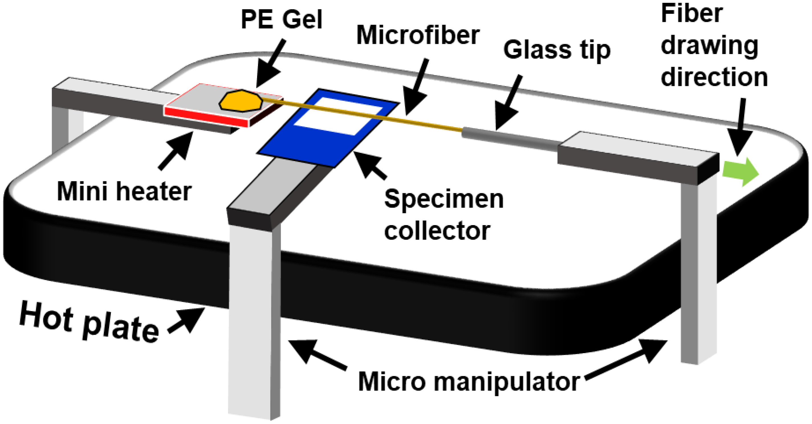
Next, we devised a two-stage tip drawing method. First a µm-scale UHMWPE fiber (MF) was drawn, as schematically represented in Figure 1. There, a 5 mm × 5 mm silicon chip with a thin film heater attached on the backside heated the gel to 120–130 °C. The temperature was measured using a thermocouple attached to the thin film heater. A hot plate placed 1 cm below the silicon chip heated the overhead air to 90 °C to prepare for hot-stretching. The translucent gel transformed to a transparent solution as it reached 130 °C. As the solution became clear, a sharp (~10 µm) glass tip was inserted into the solution using an XYZ-axis micromanipulator. It drew a MF of short length (several hundreds of µm). The drawing induces stress-induced crystallization with folded chain lamellae (kebab) on oriented chains (sheesh). Upon drawing, the lamellar structure unfolds into microfibrils that are pulled taut between entanglements [4]. During crystallization, the decalin evaporates, aided by the convective current from the hot plate. Decalin syneresis further facilitates crystallization. The fiber was then further drawn to a length of 1 cm, after which it was quenched to room temperature to minimize relaxation of the extended chain.
To manipulate and further process the microfiber, a bulk-micromachined specimen collector was fabricated by bulk micromachining processes, as detailed in Appendix A. It is a 1 cm × 3 cm silicon chip of 525 µm thickness and a square hole of 7.5 mm × 7.5 mm. Again using a standard XYZ-axis micromanipulator, the specimen collector was raised from under the drawn MF, as depicted in Figure 1, and the MF was gripped onto the specimen collector using epoxy. Because it was stretched when the specimen collector was raised and glued, the MF remained taut with a moderate tensile stress. The MF was then cut outside the collector edges.
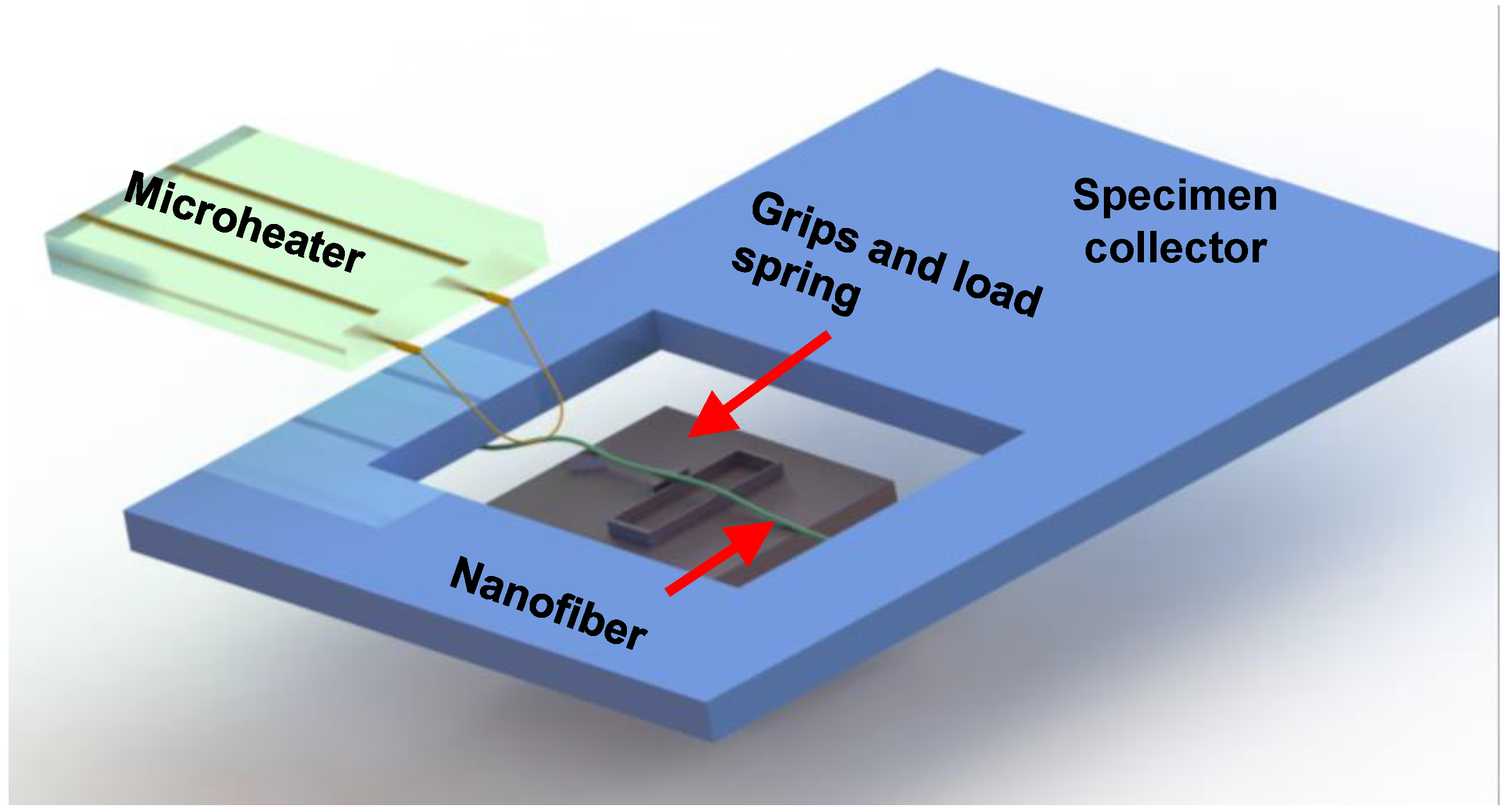
With the specimen collector acting as a carrier, the MF could now be conveniently transferred from the drawing station and positioned under an optical microscope objective. There, a locally etched and bent tungsten wire, used as a microheater, was placed in the same horizontal plane 20 µm from the MF. Details of the microheater construction are given in Appendix B.
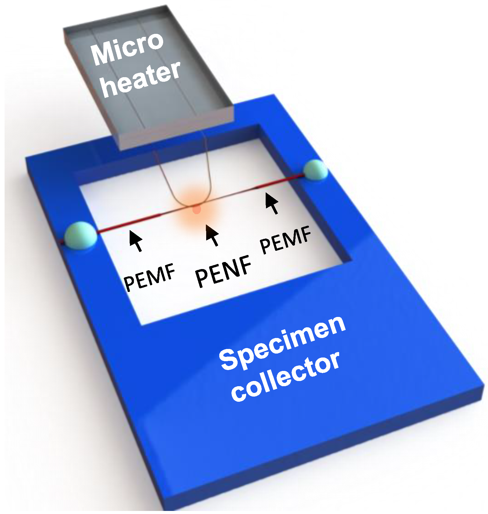
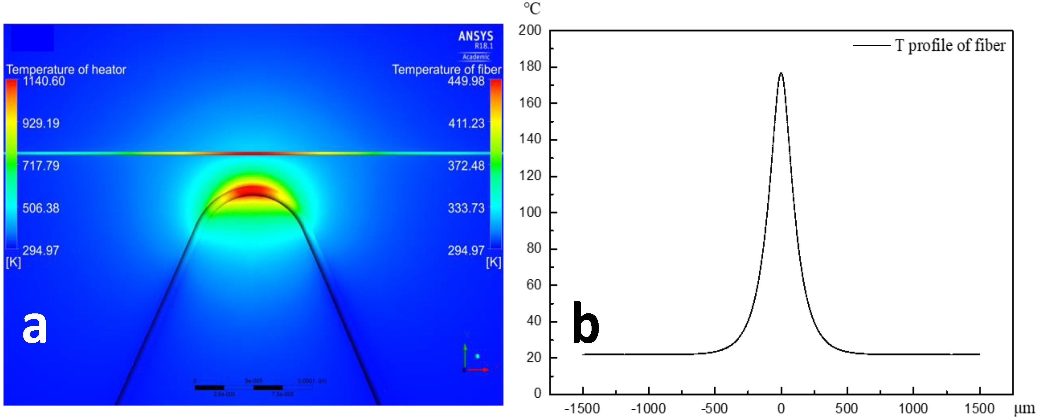
A voltage was applied to the microheater, the tungsten wire temperature increased due to Joule heating, and the collected MF was heated during a ~1 s pulse by convection to make a UHMWPE nanofiber (NF), as schematically shown in Figure 2. Most advanced thermometers have either temporal or spatial resolution limitations that limit direct temperature measurement during this process. We estimated the maximum temperature attained by the fiber during local heating using the ANSYS/FLUENT computational fluid dynamics finite element analysis software package [22]. First, the microheater temperature profile was calculated. Second, we assumed a MF with a typical 3 µm diameter and placed at a distance of 20 µm from the fiber. A potential bias 0.7 V was applied to the heater, as in the experiment. Both convective and radiative heat losses were considered. At the microscale, the boundary layer is smaller than at the macroscale. Thus, the heat transfer coefficient (h) greatly increases. Here, we used = 1000 W m−2 K−1 and emissivity = 0.1 [23]. Figure 3a shows the simulated temperature MF profile. The thermal conductivity of the MF was modeled using gel spun microfibers with = 20 W m−1 K−1 [24]. We used an emissivity value of the MF of 0.2 [25]. A constant thermal conductivity of air, = 0.02 W m−1 K−1, was used. The MF temperature reached 450 K (180 °C), and the temperature profile along the fiber is shown in Figure 3b.
During this short temperature cycle, the MF temperature likely approached the melting temperature, and stretched rapidly due to the residual tension mentioned above. As the NF developed, its molecular alignment and crystallization was further increased. This highly aligned structure was then quenched as the NF rapidly cooled after the heater was turned off. The NF, now suspended between MF regions outside the heater area, was itself typically no longer optically observable, but the outer MF regions resided in the same location as before the second drawing stage. This indicated that a NF now had been created and still physically connected the MF regions, as represented in Figure 2.
The geometrical dimensions of NFs created by this fabrication sequence were characterized by scanning electron microscopy (SEM). We found that factors influencing the diameter included the initial MF diameter, the pre-existing tensile stress, and the heater current. The diameters ranged from 20–250 nm and a length of 100 µm. Detailed specimen geometry information is provided in reference [3]. Further characterization data on twinning as determined from transmission electron microscopy and on molecular alignment as inferred from Raman spectroscopy has also been reported [3].
2.2. Positioning the Nanofibers on the Test Platforms
2.2.1. Mechanical Test Platform
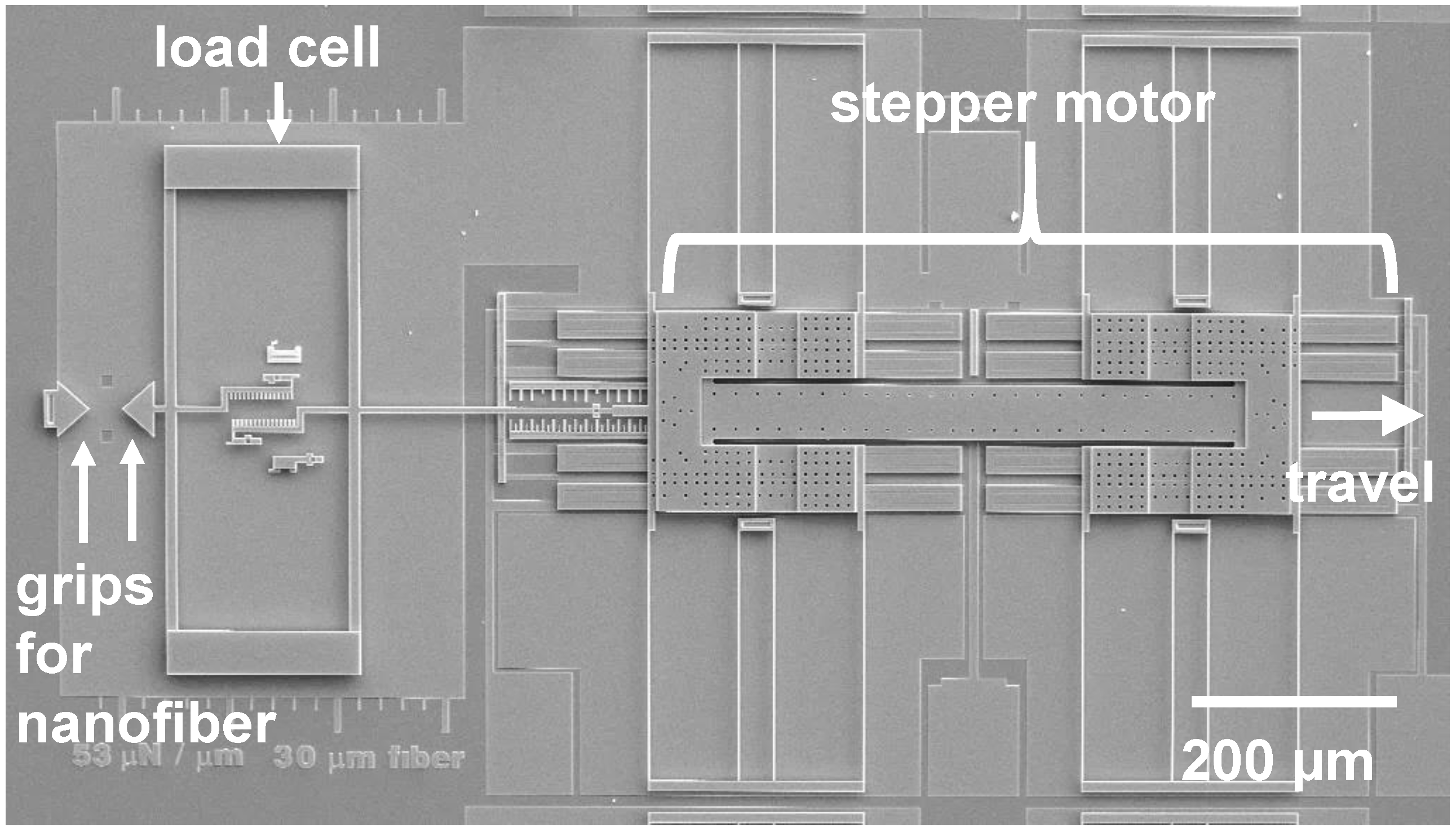
A micromachined stepper motor, detailed in [26], was selected for the mechanical measurements. The test platform was designed at Carnegie Mellon University and microfabricated by Sandia National Labs, Albuquerque, NM, USA using the SUMMiT V process [27]. The polycrystalline silicon (polysilicon) motor was “released” in the Carnegie Mellon University nanofabrication facility. The release process involves removing silicon oxide layers in hydrofluoric acid. Then a critical point drying process [28] rendered the structure freestanding. The full platform included a trailing load cell and grips, as seen on the left of Figure 4. The motor was actuated electrostatically, and each step was approximately 60 nm. Here the steps were taken at 1 Hz. It can generate an in-plane force of up to 1 mN, substantially more than the ~100 µN needed to stretch and break the NFs. Subpixel interpolation with approximately 5 nm resolution was used to measure displacements, as recorded through a 50× objective in an optical microscope. Because the load spring and the NF specimen are in series, the displacement in each depends on their relative stiffnesses. Here, the load spring stiffness was on the same order as the NFs. The tensile load was estimated by measuring the separation between the load cell combs, while the specimen extension was determined from the comb attached to the moving grip.
The minuscule sample size, the limited resolution of the optical microscope and nonlinear forces such as van der Waals, triboelectric, and capillary forces due to moisture are factors that make it difficult to successfully place nanofibers with tip-based methods. Yet, it is critical to locate and position the nanofiber precisely onto the micromachined test platform without damaging it. Electron microscopes cannot be used because of the sensitivity of polymer samples to electron beam radiation [29,30], which scissions bonds and hence degrade the mechanical and thermal property enhancement [31,32]. The manipulation by optical methods is preferred. Regarding alignment, during tensile testing, an unwanted bending moment can cause the load cell to rotate and the fiber force will be underestimated.
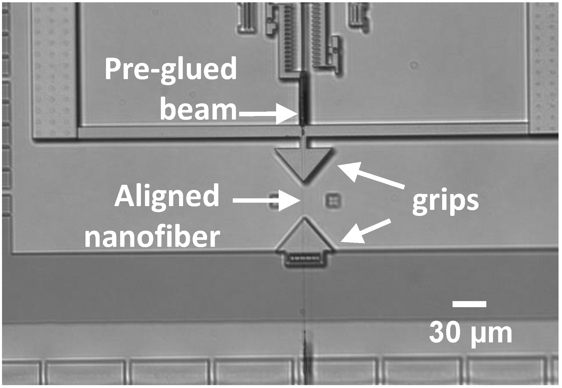
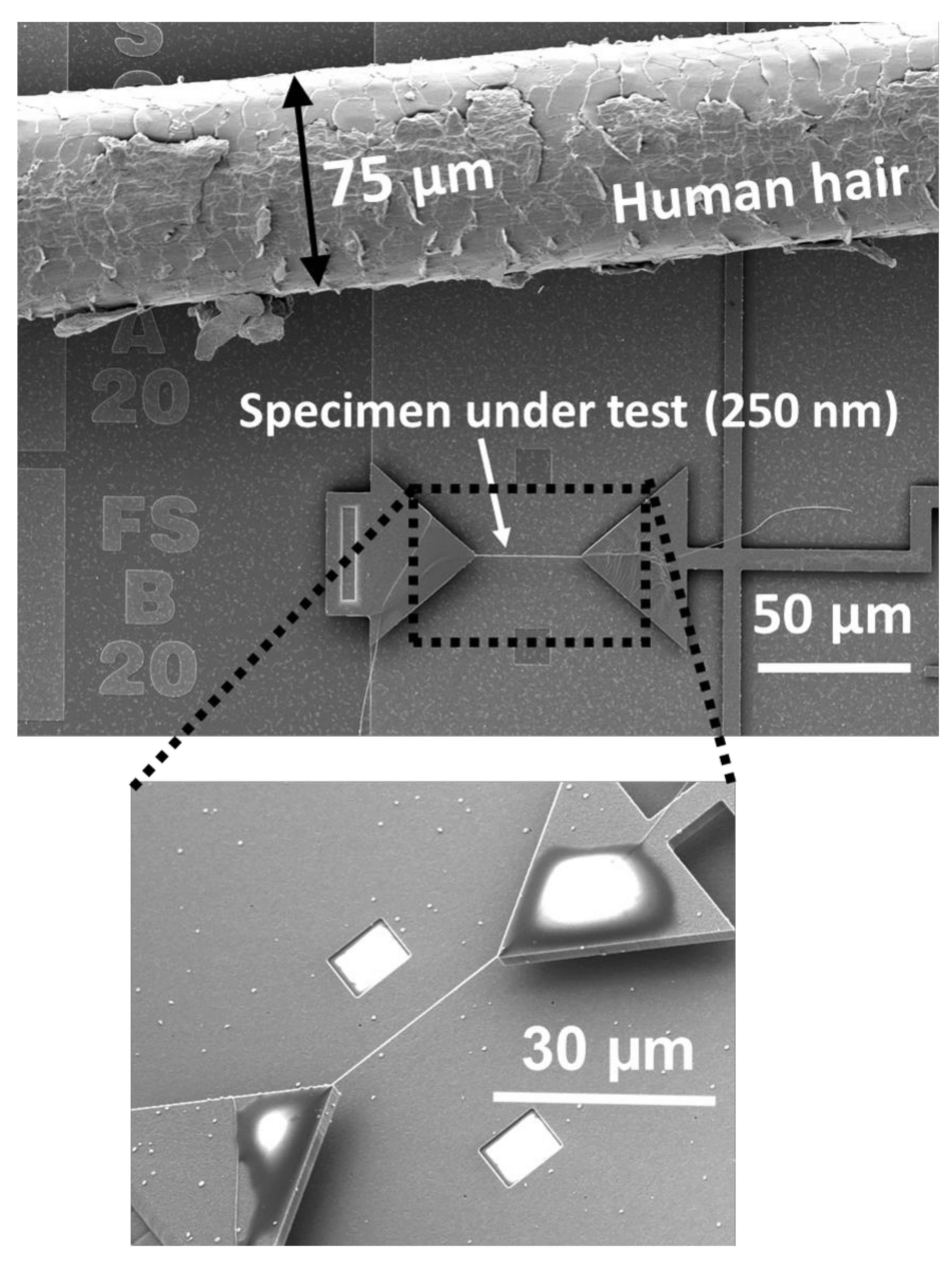
The specimen collector with a suspended NF was again used as a specimen carrier, now to align the NF with the mechanical test apparatus. It was maneuvered above the grips, as shown in Figure 5. The suspended MF in the undrawn region was used as a reference to align the nanofiber. Two triangular pads, which must grip the specimen, are behind the load spring, as seen in Figure 4. One pad is fixed to the substrate while the other is connected to the load cell. The first step in mounting the nanofiber involves pre-gluing. A small volume of cyanoacrylate glue (~20 µm × 5 µm × 5 µm) was transferred to the load cell beam that is connected to the specimen displacement-indicating comb using a compliant tungsten tip. This was maneuvered into position with a precise motorized micromanipulator. This glue held the specimen in place while the fiber was aligned and cut. The specimen collector was held by a second micromanipulator and was aligned along triangular pads under a 50× optical objective. This was done quickly (<5 min), as the glue cured in 20 min. The specimen collector was then lowered until the fiber made contact with the glue. It was fixed at that position until the glue cured enough to hold the fiber while cutting. Figure 6 shows a pre-glued PE nanofiber aligned to the grips. In this case, as in other images of fibers presented in this article, the fiber diameter is ≈250 nm so that it is optically detectable. Fibers with diameters <100 nm were also successfully mounted. Though they could not be observed optically, their presence was confirmed during mechanical or thermal testing.
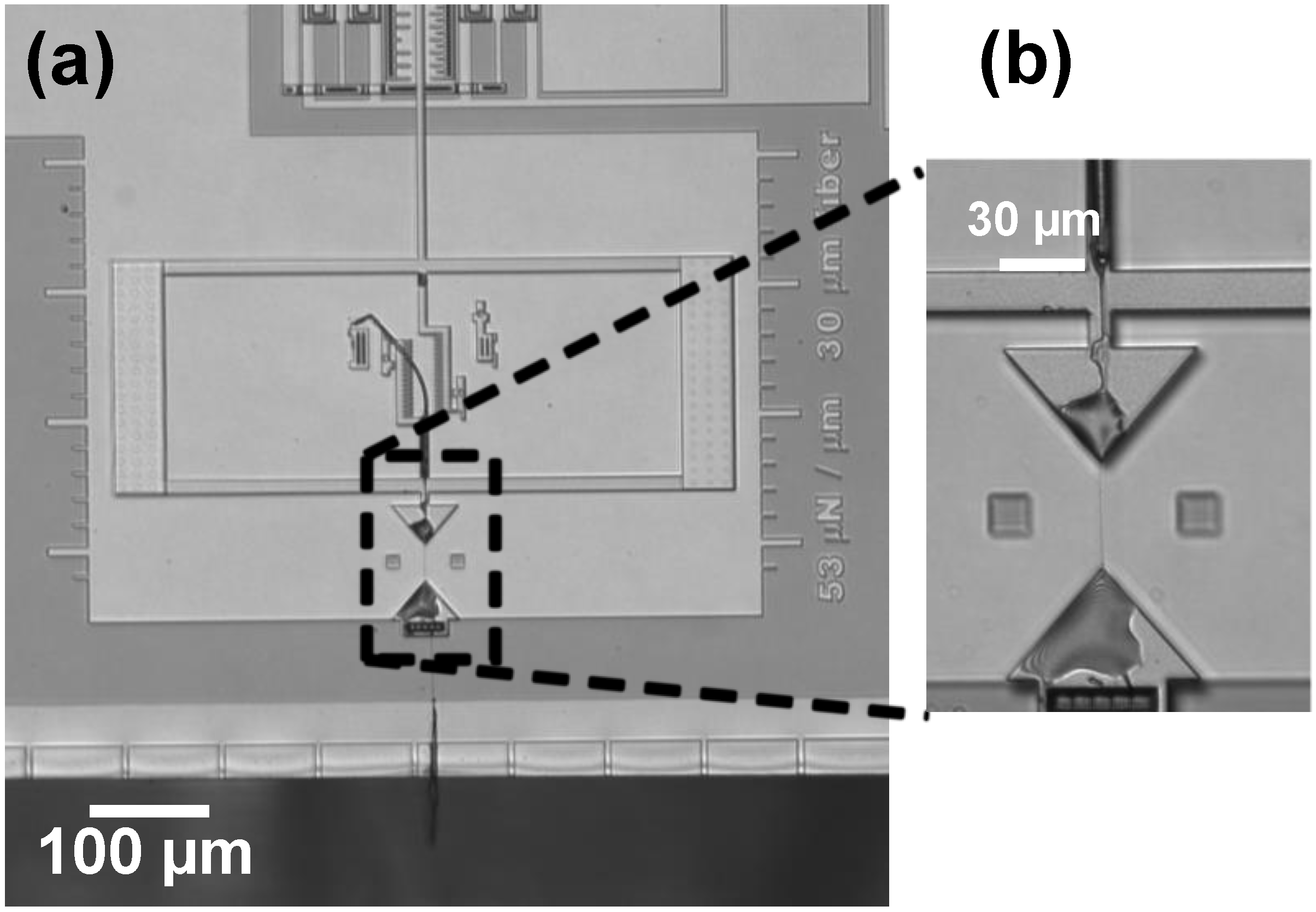
Next, the fibers were glued to the grips. Using a sharp compliant tungsten tip, glue was gently placed onto the aligned fiber over the pads. If the fiber came out of alignment, it could be nudged back into position using the same tungsten tip. As the glue became more viscous, manipulating it became more difficult and the success rate diminished. Since the working time of the glue was ~8 min, this process was completed within 6–8 min. Figure 7 shows a sample that has successfully been gripped at both ends.
After 15 min, the glue had partially cured. The microheater then cut the fiber to a length of 200–300 µm by Joule heating, much longer than the 30 µm gauge length. A DC power of 8–15 mW cut the fibers. As the heater made contact with the fiber, it melted it locally, thereby cutting it. Due to the tensile stress remaining from the specimen collector, the fiber was pulled towards the pad by a few µm. Similarly, the other end of the fiber was cut, thereby keeping the NF within the grips, with some extra length extending beyond the glue.
After a fiber had been glued, it was cured in laboratory air for 48 h, and was then ready for testing. Figure 8 shows a SEM image of a gripped nanofiber in the mechanical platform.
2.2.2. Thermal Test Platform
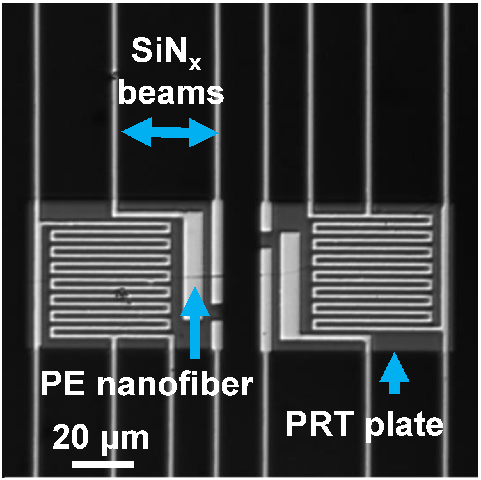
A different microdevice, consisting of suspended platinum resistance thermometers (PRTs) was used to conduct thermal characterization [33]. A total of seven SiNx beams, with platinum deposited on each, supports each of two suspended SiNx plates. Serpentine platinum coils are fabricated on top of the SiNx plates and are connected to electrical pads in a supported region. A lock-in amplifier detects small changes in the resistance of these PRTs. Consequently, the device is sensitive to minute temperature changes. A NF connecting one platform to the adjacent one conducts heat from the heated side to the sensing side. Details of the measurement system are given in reference [33].
The alignment of the nanofiber to the plates was similar to that discussed above for the mechanical device. However, it was found that epoxy glues wetted the Pt wire surface, creating an insulating layer that significantly increased the thermal contact resistance, . Without glue, the cutting process tended to pull the nanofiber off the suspended plates. Focused ion beam (FIB)-deposited Pt would likewise reduce the crystallinity and significantly increase the thermal resistance.
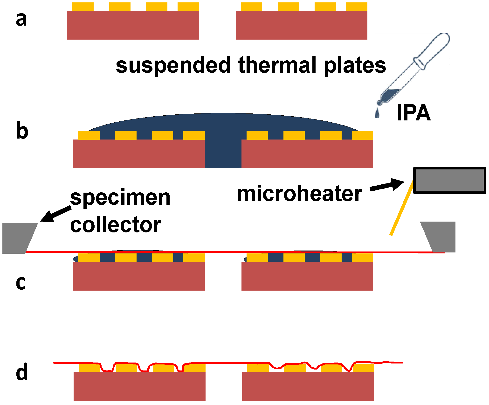
To solve this problem, we took advantage of the surface tension from evaporating isopropanol (IPA), which was able to affix the fiber onto the substrate. As the liquid evaporated, it pulled the fiber into contact with the plates and created sufficient adhesion to keep the nanofiber in place during the cutting process. This adhesion process was termed “capillary-assisted adhesion” and is discussed next.
Steps to achieve capillary-assisted adhesion are schematically shown in Figure 9. In this process, an IPA liquid drop was first placed on top of the thermal device (Figure 9b). Evaporation of IPA from the device was closely monitored under the optical microscope. After the liquid meniscus connecting the suspended plates broke, the suspending beams (not shown) cause the plates to separate to their nominal 5–10 µm gap. Before the liquid layer evaporated from the surface of the plates, a pre-aligned nanofiber was expeditiously lowered into focus and contact was made with the pads (Figure 9c). The liquid wet the fiber and the evaporating liquid surface pulled the fiber down due to surface tension. The fiber then adhered to the pads (Figure 9d). This surface tension, accompanied by the van der Waals force, increased the contact width of the fiber on the pads. Also, the fiber conformed to the undulating surface, increasing the contact length significantly. Increased contact width and contact length due to capillary-assisted adhesion reduced the thermal contact resistance. Figure 10 shows an optical image of a mounted nanofiber on the device. NFs that are of a significantly smaller diameter and not resolvable under the optical microscope could be manipulated and mounted onto the test platform.
3. Results and Discussion
3.1. Calibration of Mechanical Test Platform Using Silica Fibers
Silica nanofibers were used to validate the nanomechanical measurements reported in [3]. They were prepared using a flame brushing technique [34], where a silica microwire was heated in the center using a butane torch and pulled at other two ends. It was stretched until broken; nanofibers were then obtained. The nanofiber was placed on a PDMS substrate, and in this case, conventional manipulation methods were used to mount the fiber. A tungsten tip with a tip of 1 µm diameter connected to a high precision micro-manipulator was used to manipulate the silica nanofiber sample from the PDMS to the mechanical test platform. Cyanoacrylate glue was used to attach the silica nanofiber to the grips.
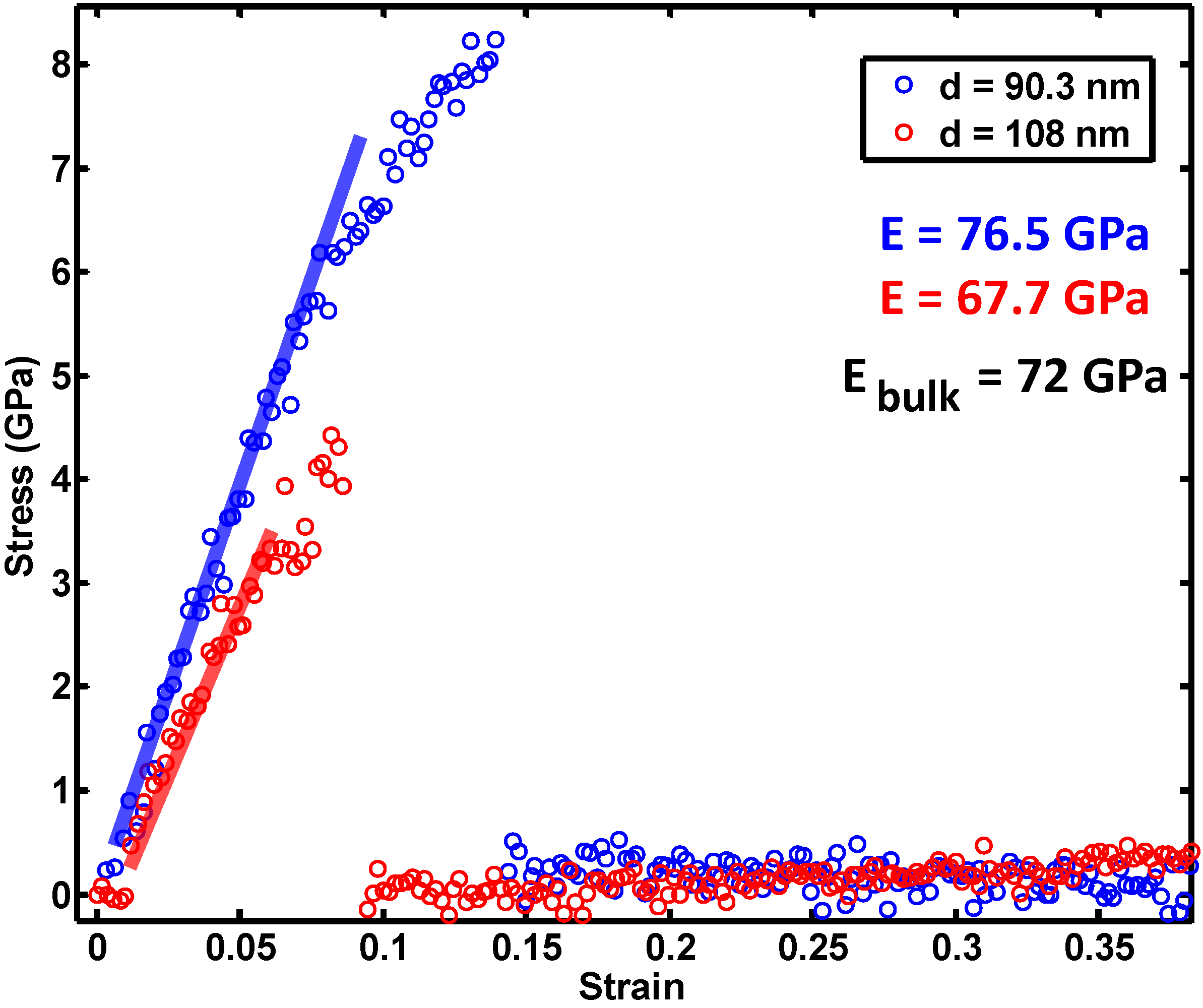
Stress and strain were obtained from the force normalized over the cross-section diameter and elongation over the gauge length. Figure 11 shows the stress–strain curve of a silica nanofiber of diameter 108 nm. The Young’s modulus was obtained from the slope of the stress–strain curve in the elastic region. For that fiber, it was found to be 67.7 GPa. The strength was 4.5 GPa and its elongation at failure was 9%. A second silica nanofiber was also tested with diameter = 90 nm (Figure 11). The Young’s modulus value was 76.5 GPa, while the ultimate strength was 8.2 GPa, twice that of the previous sample. Elongation at failure was also observed to be higher than the previous sample at 13.8%.
The Young’s modulus values are similar to that of bulk silica (72 GPa) [35]. Silva et al. tested silica nanofibers using an AFM cantilever bending test and found that silica nanofiber Young’s modulus for diameters larger than 280 nm was similar to bulk [35]. Wang et al. [36] obtained 27 ± 7 GPa for diameters between 43 nm and 95 nm and Dickin et al. [37] obtained 47 ± 7 GPa for diameters between 80 nm and 98 nm. These measurements were done in the TEM using a resonance method. Recent work [38] on a tensile test of silica nanofibers of dimensions 33.9 nm and 18.7 nm under TEM found that Young’s modulus was about 77.6 GPa, close to bulk silica. The values in Figure 11 are in good agreement with the bulk value and with much of the literature.
The strengths are much higher than bulk silica (0.2 GPa) [39]. This is because of nanoscale size effect, where flaw density is significantly reduced and the probability of having a flaw larger than critical flaw is minimal. However, our values of silica nanofiber strength are somewhat lower than that of reference [39], where an average strength of 10 GPa was measured. Our fabrication method of using butane torch and strength test in high relative humidity (~70%) introduces hydroxyl groups in the silica surface that may degrade the silica sample [39,40].
We observed elongation as high as 13.8% in the silica nanofibers. However, SEM imaging of the fractured glass fiber shows a flat fracture surface, consistent with brittle failure. It is likely that the glue slipped to a small degree as failure was approached, as the curve deviated from linearity. However, this only affects the penultimate portion of the stress–strain curve. From this data, it is apparent that the test platform can measure strength and strain if the specimen is firmly gripped.
3.2. Gripping the UHMWPE Nanofibers in Mechanical Testing
For UHMWPE nanofibers, initial test results revealed more severe slip at the grips before their strength was reached. The surface energy of PE is low (31 mJ m−2) and the absence of a polar component (similar to PTFE, 19 mJ m−2) makes it difficult to wet with adhesives [41,42]. There are many commercial including Loctite 3032, Loctite 3035, Scotch weld DP 8005, Scotch weld DP 8010, Loctite plastic bonding system, and TAP poly-weld. They are designed for low surface energy olefins such as polyethylene and polypropylene. However, their viscosity, working life, and/or requirement to surface treat the sample made them unsuitable for this work. All available glues were tried. All slipped to some degree.
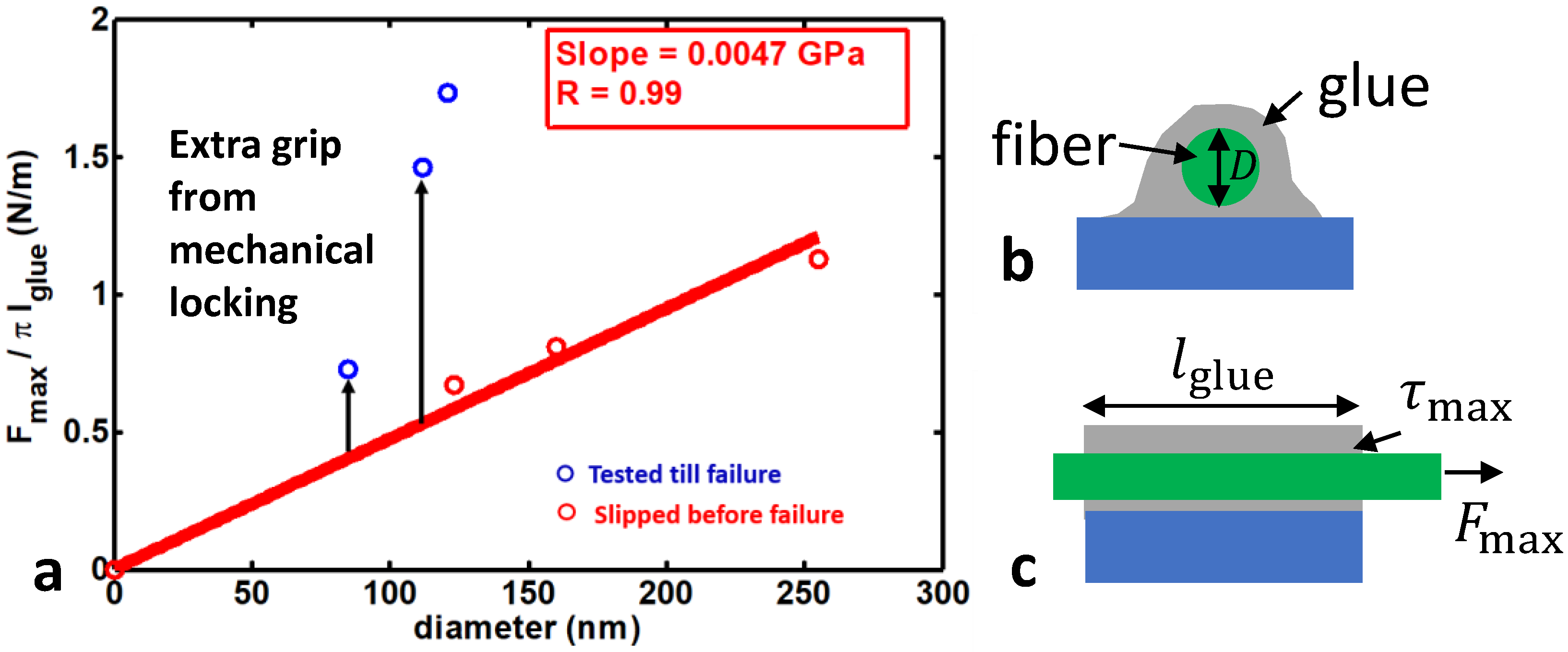
Six ultra-drawn NFs with diameters ranging from 85 nm to 255 nm were tested with Loctite® AA 3032/Henkel, which is a specialized glue for PE and was found to be the best glue for this work. From composites theory [43], the maximum force () applied to a specimen of diameter before it slips can be used to obtain the average interface shear strength, . Accordingly,
which can be rewritten as
Here, lglue is the length of the nanofiber/glue interface. In Figure 12a, is plotted against . The slope of specimens that slipped before failure, as indicated by the red circles, is 4.7 MPa. This corresponds to . Indeed, video images taken during the testing revealed the slip directly. The value compares reasonably well with the shear strength of Loctite® AA 3032/Henkel, (6 MPa with high density PE). On the other hand, specimens tested until failure (blue circles in Figure 12a) displayed a significantly higher force per unit length. The additional gripping force was contributed by a mechanical locking procedure, as described in [3]. Figure 12b,c shows the schematic of fiber within the glue.
From this data, we can estimate the length of the glued/fiber interface required to grip a typical 100 nm NF at a uniaxial stress of 10 GPa, on par with the tensile strength, . Then, 4 ≈ 53 µm. The gripper length was 30 µm. With greater lengths, it should be possible to test UHMWPE nanofiber specimens to failure without the mechanical locking procedure, and thereby also assess Young’s modulus.
3.3. Thermal Contact Resistance
Thermal contact resistance between the sample and the islands will result in an incorrect thermal conductivity value if not correctly assessed. Furthermore, if is much larger than the intrinsic thermal resistance of nanofiber, , the procedure is subject to large errors. The total thermal resistance at steady state is the sum of thermal contact resistances, 2, and . Then,
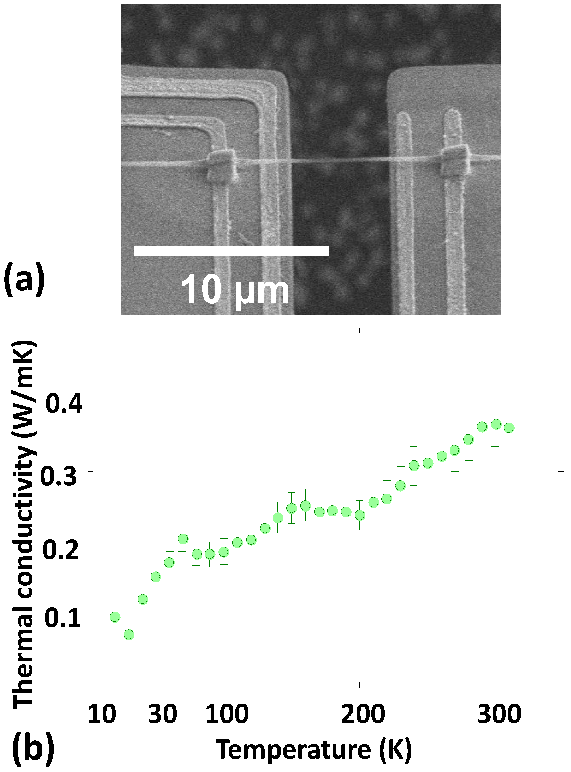
For high thermal conductivity samples, such as UHMWPE nanofibers, can be increased by making the nanofiber long and the cross-section area small. However, this will also reduce the heat flux significantly. Consequently, the temperature rise of sensing side will be lessened, making accurate measurement difficult. A platinum or graphite coating, using electron beam or focused ion beam (FIB), has been extensively used in literature to reduce thermal contact resistance [44,45]. However, high-energy electron/ion beam amorphized the NFs and reduced the thermal conductivity down to the bulk value, as shown in Figure 13. There, data is shown over a wide temperature range, but the extracted thermal conductivities of 0.1 to 0.4 W/mK are very low. A better approach is to obtain a condition in which . Values from 60–90 W/mK [3], on par with metals, were measured for NFs attached by the capillary-assisted adhesion method described in Section 2.2.2.
4. Summary and Conclusions
Polymer nanofibers may possess properties much higher than their bulk counterparts, and therefore accurate assessment of these properties is of great interest. However, because of their small size and the omnipresence of van der Waals, electrostatic and capillary forces, it is often difficult to manipulate individual polymer nanofibers on to test platforms that measure their properties. Here, we have detailed the fabrication (Appendix A) and use (Section 2.2.2) of a specimen collector (Figure 1, Figure 2 and Figure 5), which makes it possible to position nanofibers within ±1 µm of the desired location (Figure 6, Figure 7 and Figure 8) without exposing them to damaging electron beam irradiation. Even after they are in place, the very high strength and low surface energy of UHWMPE nanofiber render grip strength an obstacle to accurate mechanical testing results (Figure 12). This issue can be surmounted by gripping outside the smallest nanofiber region if extra material has accumulated there. Alternatively, longer grip regions may be effective. With respect to thermal measurements, contact resistance can dominate the values (Figure 13). We have found that a capillary-assisted technique (Figure 9) can significantly reduce contact resistance without damage to the nanofiber. While we find these procedures to be helpful, further manipulation improvements will surely be welcomed by practitioners.
Author Contributions
Conceptualization, all the authors; Investigation, R.S.; Writing—Original Draft Preparation, M.P.d.B.; Writing—Review & Editing, R.S. and M.P.d.B.; Supervision, S.S. and M.P.d.B.
Funding
This work was supported by the US National Science Foundation (NSF) under award CMMI-1334630.
Acknowledgments
We thank Kedar Hippalgaonkar (Institute of Materials Research and Engineering (IMRE), Singapore) for providing us with thermal platform.
Conflicts of Interest
The authors declare no conflict of interest.
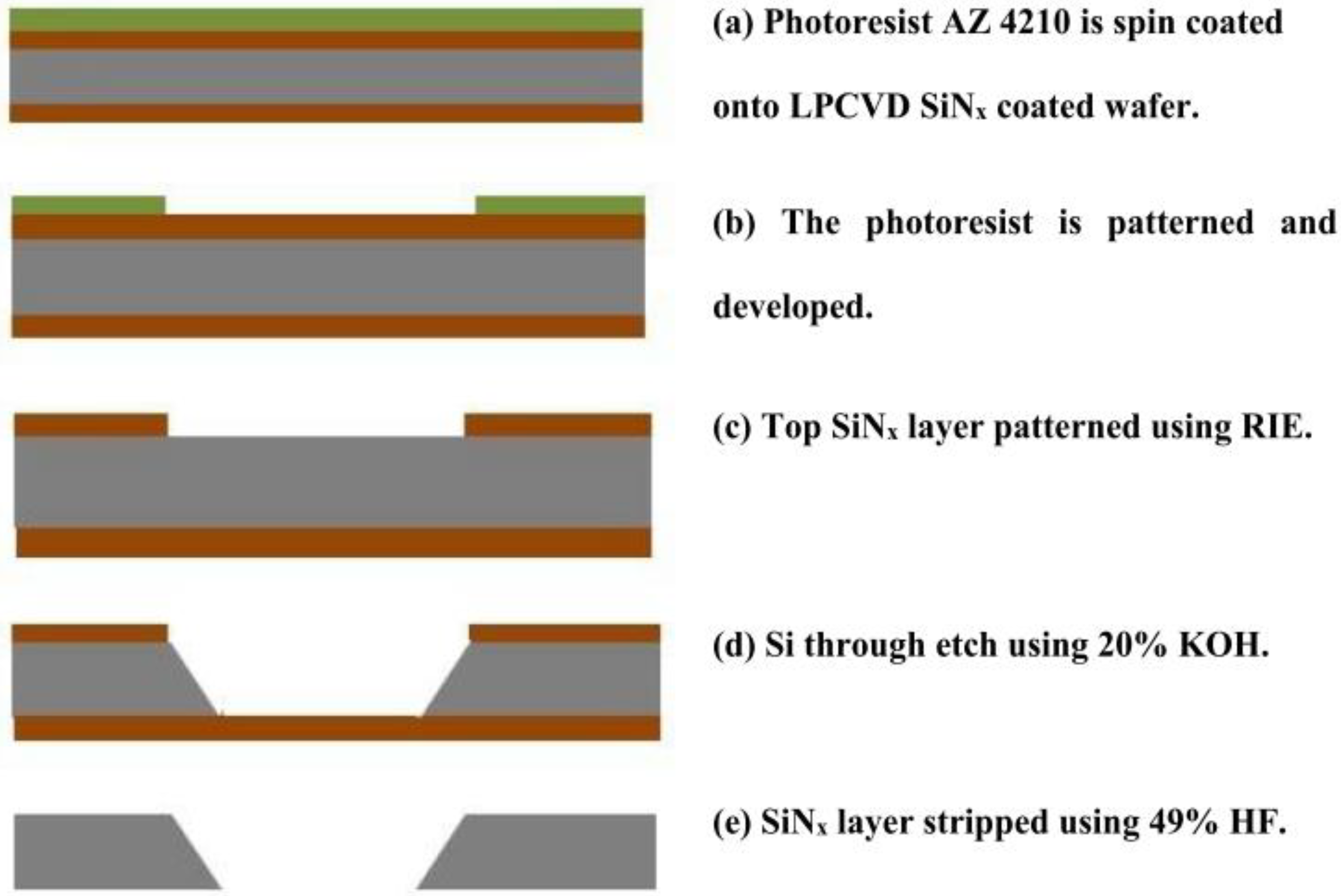
Appendix A. Specimen Collector Fabrication
The specimen collector was fabricated by bulk micromachining techniques, as shown in Figure A1. The selectivity of a traditional oxide mask for silicon etching is insufficient for a through etch. Four-inch (100)-oriented silicon wafers coated with a 300 nm LPCVD silicon nitride (SiNx) film on both sides were purchased from WRS materials. The wafers were HMDS vapor-primed at 150 °C for 5 min to promote photoresist adhesion. AZ 4210 photoresist was spin-coated at 4000 rpm, resulting in a 2.1 µm thick layer. This was followed by a soft bake at 95 °C for 1 min.
Figure A1.
Micro fabrication processes of the sample collector.

The photoresist was patterned using a Karl Suss MA6 aligner with ultraviolet light of 320 nm wavelength at 5 mW/cm2 for 80 s. The exposed photoresist was then developed by a 1:4 mixture of AZ 400K and deionized (DI) water for 120 s. The wafer was then cleaned in DI water and dried with nitrogen.
The photoresist pattern was transferred into the SiNx by reactive ion etching (RIE) using a Plasmatherm 790 RIE system. A gas mixture of tetrafluoromethane (CF4) and oxygen (O2) at flow rates of 19.5 sccm and 0.5 sccm, respectively and a total pressure of 35 mT. An RF power of 60 watts at a bias of 315 volts was applied to induce plasma. The fluorine in CF4 reacts with the silicon in silicon nitride to form volatile silicon tetrafluoride (SiF4). Carbon can form polymer deposit onto the surface, reducing the etch rate. Hence, the fluorine/carbon ratio determines the SixNy etch rate. A higher ratio provides a higher etch rate. Oxygen can react with the carbon forming volatile gas, which increases the fluorine to carbon ratio and thus increase the reaction rate. However, oxygen also etches the photoresist, so an optimum ratio must be found. We obtained an average etch rate of 26 nm/min but the etch rate decreased over the time due to the polymer deposit. After 6 min, the etching was stopped and argon gas was used to purge the chamber for 2 min at 200 mT. This was done to eliminate polymer deposit that would otherwise hinder the SiN etching. The total duration was 12.5 min to ensure all silicon nitride had been etched. Oxygen plasma was then applied for 5 min at 50 mT and 100 W to ash the photoresist and remove any residual polymer. The chamber was once again purged with argon at 200 mT for 2 min. The wafer samples were then cleaned using acetone, isopropanol alcohol and DI water, respectively.
The wafer was now through-etched using KOH according to SiNx. pattern. KOH etching depends on the crystal orientation of silicon, the solution concentration and the temperature. Here, KOH pellets were mixed with DI water to obtain 20% solution, an optimum concentration for (100) Si etching [46]. The solution was heated to 80 °C and the wafer was placed in the solution, whereupon hydrogen bubbles, indicative of the etching, were immediately observed. The glassware was covered with aluminum foil to reduce evaporative loss, thereby reducing the KOH concentration increase as the vapor re-condensed into the solution. However, the foil reacted with the vapor and some holes were produced. The total etch duration was 7 h for an average etch rate of 78.5 µm/h, less than the reported etch rate for 20% KOH at 80 °C [46], likely due to the increasing concentration. Etching ceased at the bottom SiNx layer. KOH etching is an anisotropic etch with the (111) plane etching more slowly than the (110) and (100) planes, resulting in a characteristic pyramid like structure with 54.7° [46]. At the end of KOH etch, we obtained square holes with the expected 54.7° slanted walls. The wafer was rinsed in DI water, and the remaining SiNx material on the top and bottom was removed after 15 min in 49% hydrofluoric acid (HF). The wafer was then diced into individual specimen collectors.
Appendix B. Microheater Construction
The micro heater is a sharply bent tungsten wire locally etched at the tip to 5–10 µm. It is joule-heated to a temperature exceeding 500 °C (Figure 3) at its tip to locally transform a MF into a NF. It was constructed and assembled as follows: Tungsten wire of 50 µm diameter was purchased from ESPI metals, cut to a 10 cm length, bent near its center, and adhered to a glass slide. The protruding bent edge was submerged in a beaker with 30% H2O2 solution that was held at room temperature while it was stirred magnetically. The wire was etched until the final diameter at the tip reached 5–10 µm as shown in Figure A2a. The ends of the wire were attached with copper tape for electrical attachment. Figure A2b shows a fabricated microheater.
Figure A2.
Microheater used for local heat stretching and cutting PE fiber. (a) microheater (b) tungsten tip of microheater with diameter ~3 μm.
Figure A2.
Microheater used for local heat stretching and cutting PE fiber. (a) microheater (b) tungsten tip of microheater with diameter ~3 μm.

References
- Naraghi, M.; Chasiotis, I.; Kahn, H.; Wen, Y.; Dzenis, Y. Novel method for mechanical characterization of polymeric nanofibers. Rev. Sci. Instrum. 2007, 78, 85108. [Google Scholar] [CrossRef] [PubMed] [Green Version]
- Li, P.; Hu, L.; McGaughey, A.J.H.; Shen, S. Crystalline polyethylene nanofibers with the theoretical limit of Young’s modulus. Adv. Mater. 2014, 26, 1065–1070. [Google Scholar] [CrossRef] [PubMed]
- Shrestha, R.; Li, P.; Chatterjee, B.; Zheng, T.; Wu, X.; Liu, Z.; Luo, T.; Choi, S.; Hippalgaonkar, K.; de Boer, M.P.; et al. Crystalline polymer nanofibers with ultra-high strength and thermal conductivity. Nat. Commun. 2018, 9, 1664. [Google Scholar] [CrossRef] [PubMed]
- Shen, S.; Henry, A.; Tong, J.; Zheng, R.; Chen, G. Polyethylene nanofibres with very high thermal conductivities. Nat. Nanotechnol. 2010, 5, 251–255. [Google Scholar] [CrossRef] [PubMed]
- Zhong, Z.; Wingert, M.C.; Strzalka, J.; Wang, H.H.; Sun, T.; Wang, J.; Chen, R.; Jiang, Z. Structure-induced enhancement of thermal conductivities in electrospun polymer nanofibers. Nanoscale 2014, 6, 8283–8291. [Google Scholar] [CrossRef] [PubMed]
- Singh, V.; Bougher, T.L.; Weathers, A.; Cai, Y.; Bi, K.; Pettes, M.T.; McMenamin, S.A.; Lv, W.; Resler, D.P.; Gattuso, T.R.; et al. High thermal conductivity of chain-oriented amorphous polythiophene. Nat. Nanotechnol. 2014, 9, 384–390. [Google Scholar] [CrossRef] [PubMed]
- Agarwal, S.; Wendorff, J.H.; Greiner, A. Progress in the Field of Electrospinning for Tissue Engineering Applications. Adv. Mater. 2009, 21, 3343–3351. [Google Scholar] [CrossRef] [PubMed]
- Chronakis, I.S. Novel nanocomposites and nanoceramics based on polymer nanofibers using electrospinning process—A review. J. Mater. Process. Technol. 2005, 167, 283–293. [Google Scholar] [CrossRef]
- Huang, Z.M.; Zhang, Y.Z.; Kotaki, M.; Ramakrishna, S. A review on polymer nanofibers by electrospinning and their applications in nanocomposites. Compos. Sci. Technol. 2003, 63, 2223–2253. [Google Scholar] [CrossRef]
- Fang, J.; Niu, H.; Lin, T.; Wang, X. Applications of electrospun nanofibers. Sci. Bull. 2008, 53, 2265–2286. [Google Scholar] [CrossRef]
- Calderón, M.Á.R.; Zhao, W. Applications of Polymer Nanofibers in Bio-Materials, Biotechnology and Biomedicine: A Review. In TMS 2014: 143rd Annual Meeting & Exhibition; Springer International Publishing: Cham, Switzerland, 2014; pp. 401–414. [Google Scholar]
- Fu, Y.Q.; Luo, J.K.; Flewitt, A.J.; Milne, W.I. Smart microgrippers for bioMEMS applications. MEMS Biomed. Appl. 2012, 291–336. [Google Scholar] [CrossRef]
- Bøggild, P. Nanogrippers. In Encyclopedia of Nanotechnology; Bhushan, B., Ed.; Springer: New York, NY, USA, 2015. [Google Scholar]
- Agnus, J.; Nectoux, P.; Chaillet, N. Overview of microgrippers and design of a micro-manipulation station based on a MMOC microgripper. In Proceedings of the 2005 IEEE International Symposium on Computational Intelligence in Robotics and Automation, Espoo, Finland, 27–30 June 2005. [Google Scholar]
- Soltani, M.; Lin, J.; Forties, R.A.; Inman, J.T.; Saraf, S.N.; Fulbright, R.M.; Lipson, M.; Wang, M.D. Nanophotonic trapping for precise manipulation of biomolecular arrays. Nat. Nanotechnol. 2014, 9, 448–452. [Google Scholar] [CrossRef] [PubMed] [Green Version]
- Nam, A.S.; Amon, C.; Sitti, M. Three-dimensional nanoscale manipulation and manufacturing using proximal probes: Controlled pulling of polymer micro/nanofibers. In Proceedings of the IEEE International Conference on Mechatronics (ICM’04), Istanbul, Turkey, 5 June 2004; pp. 224–230. [Google Scholar]
- Wingert, M.C.; Jiang, Z.; Chen, R.; Cai, S. Strong size-dependent stress relaxation in electrospun polymer nanofibers. J. Appl. Phys. 2017, 121, 015103. [Google Scholar] [CrossRef] [Green Version]
- Egerton, R.F.; Li, P.; Malac, M. Radiation damage in the TEM and SEM. Micron 2004, 35, 399–409. [Google Scholar] [CrossRef] [PubMed]
- Doshi, J.; Reneker, D.H. Electrospinning process and applications of electrospun fibers. J. Electrostat. 1995, 35, 151–160. [Google Scholar] [CrossRef]
- Reneker, D.H.; Chun, I. Nanometre diameter fibres of polymer, produced by electrospinning. Nanotechnology 1996, 7, 216–223. [Google Scholar] [CrossRef]
- Shi, X.M.; Bin, Y.Z.; Hou, D.S.; Men, Y.F.; Matsuo, M. Gelation/crystallization mechanisms of UHMWPE solutions and structures of ultradrawn gel films. Polym. J. 2014, 46, 21–35. [Google Scholar] [CrossRef]
- Features of ANSYS Fluent. Available online: http://www.ansys.com/products/fluids/ansys-fluent/ansys-fluent-features (accessed on 14 January 2018).
- Narayanaswamy, A.; Gu, N. Heat Transfer from Freely Suspended Bimaterial Microcantilevers. J. Heat Transf. 2011, 133, 042401. [Google Scholar] [CrossRef]
- DSM Dyneema Fact Sheet. Available online: http://www.pelicanrope.com/pdfs/Dyneema-Comprehensive-factsheet-UHMWPE.pdf (accessed on 14 January 2018).
- Fujikura, Y.; Suzuki, T.; Matsumoto, M. Emissivity of chlorinated polyethylene. J. Appl. Polym. Sci. 1982, 27, 1293–1300. [Google Scholar] [CrossRef]
- Shroff, S.S.; de Boer, M.P. Constant Velocity High Force Microactuator for Stick-Slip Testing of Micromachined Interfaces. J. Microelectromech. Syst. 2015, 24, 1868–1877. [Google Scholar] [CrossRef]
- Sniegowski, J.J.; de Boer, M.P. IC-Compatible Polysilicon Surface Micromachining. Annu. Rev. Mater. Sci. 2000, 30, 299–333. [Google Scholar] [CrossRef]
- Weibel, G.L.; Ober, C.K. An overview of supercritical CO2 applications in microelectronics processing. Microelectron. Eng. 2003, 65, 145–152. [Google Scholar] [CrossRef]
- Sawyer, L.C.; Grubb, D.T.; Meyers, G.F. Polymer Microscopy; Springer: New York, NY, USA, 2008; ISBN 978-0-387-72627-4. [Google Scholar]
- Revol, J.F.; Manley, R.S.J. Lattice imaging in polyethylene single crystals. J. Mater. Sci. Lett. 1986, 5, 249–251. [Google Scholar] [CrossRef]
- Ma, J.; Zhang, Q.; Mayo, A.; Ni, Z.; Yi, H.; Chen, Y.; Mu, R.; Bellan, L.M.; Li, D. Thermal conductivity of electrospun polyethylene nanofibers. Nanoscale 2015, 7, 16899–16908. [Google Scholar] [CrossRef] [PubMed]
- Naraghi, M.; Ozkan, T.; Chasiotis, I.; Hazra, S.S.; de Boer, M.P. MEMS platform for on-chip nanomechanical experiments with strong and highly ductile nanofibers. J. Micromech. Microeng. 2010, 20, 125022. [Google Scholar] [CrossRef]
- Li, D.; Wu, Y.; Kim, P.; Shi, L.; Yang, P.; Majumdar, A. Thermal conductivity of individual silicon nanowires. Appl. Phys. Lett. 2003, 83, 2934–2936. [Google Scholar] [CrossRef]
- Tong, L.; Gattass, R.R.; Ashcom, J.B.; He, S.; Lou, J.; Shen, M.; Maxwell, I.; Mazur, E. Subwavelength-diameter silica wires for low-loss optical wave guiding. Nature 2003, 426, 816–819. [Google Scholar] [CrossRef] [PubMed]
- Silva, E.C.C.M.; Tong, L.; Yip, S.; Van Vliet, K.J. Size Effects on the Stiffness of Silica Nanowires. Small 2006, 2, 239–243. [Google Scholar] [CrossRef] [PubMed]
- Wang, Z.; Gao, R.; Poncharal, P.; De Heer, W.; Dai, Z.; Pan, Z. Mechanical and electrostatic properties of carbon nanotubes and nanowires. Mater. Sci. Eng. C 2001, 16, 3–10. [Google Scholar] [CrossRef]
- Dikin, D.A.; Chen, X.; Ding, W.; Wagner, G.; Ruoff, R.S. Resonance vibration of amorphous SiO2 nanowires driven by mechanical or electrical field excitation. J. Appl. Phys. 2003, 93, 226–230. [Google Scholar] [CrossRef]
- Luo, J.; Wang, J.; Bitzek, E.; Huang, J.Y.; Zheng, H.; Tong, L.; Yang, Q.; Li, J.; Mao, S.X. Size-Dependent Brittle-to-Ductile Transition in Silica Glass Nanofibers. Nano Lett. 2016, 16, 105–113. [Google Scholar] [CrossRef] [PubMed]
- Brambilla, G.; Payne, D.N. The Ultimate Strength of Glass Silica Nanowires. Nano Lett. 2009, 9, 831–835. [Google Scholar] [CrossRef] [PubMed]
- Armstrong, J.L.; Matthewson, M.J.; Kurkjian, C.R. Humidity Dependence of the Fatigue of High-Strength Fused Silica Optical Fibers. J. Am. Ceram. Soc. 2000, 83, 3100–3109. [Google Scholar] [CrossRef] [Green Version]
- Owens, D.K.; Wendt, R.C. Estimation of the surface free energy of polymers. J. Appl. Polym. Sci. 1969, 13, 1741–1747. [Google Scholar] [CrossRef]
- Brewis, D.M.; Briggs, D. Adhesion to polyethylene and polypropylene. Polymer 1981, 22, 7–16. [Google Scholar] [CrossRef]
- Chawla, K.K. Ceramic Matrix Composites. In Composite Materials; Springer: New York, NY, USA, 1998; pp. 212–251. [Google Scholar]
- Yu, C.; Saha, S.; Zhou, J.; Shi, L.; Cassell, A.M.; Cruden, B.A.; Ngo, Q.; Li, J. Thermal Contact Resistance and Thermal Conductivity of a Carbon Nanofiber. J. Heat Transf. 2006, 128, 234–239. [Google Scholar] [CrossRef]
- Cheng, Z.; Liu, L.; Xu, S.; Lu, M.; Wang, X. Temperature Dependence of Electrical and Thermal Conduction in Single Silver Nanowire. Sci. Rep. 2015, 5, 10718. [Google Scholar] [CrossRef] [PubMed] [Green Version]
- Seidel, H.; Csepregi, L.; Heuberger, A.; Baumgärtel, H. Anisotropic Etching of Crystalline Silicon in Alkaline Solutions. J. Electrochem. Soc. 1990, 137, 3612–3626. [Google Scholar] [CrossRef]
Figure 1.
Schematic of tip drawing setup.

Figure 2.
Schematic of the specimen collector and the fabrication of an ultra-high molecular weight polyethylene (UHMWPE) nanofiber (NF). Adapted from reference [3] supplementary information.
Figure 2.
Schematic of the specimen collector and the fabrication of an ultra-high molecular weight polyethylene (UHMWPE) nanofiber (NF). Adapted from reference [3] supplementary information.

Figure 3.
Temperature profile of the W wire heater and the polyethylene microfiber (MF) from an ANSYS/FLUENT simulation. (a) Temperature map of the heater and the MF. (b) Plot of the MF temperature profile. The maximum temperature reaches 450 K (180 °C). Adapted from reference [3] supplementary information.

Figure 4.
The micromachined test platform used for mechanical measurements.

Figure 5.
Schematic of alignment of the NF along the platform grips (figure not to scale). Adapted from reference [3] supplementary information.
Figure 5.
Schematic of alignment of the NF along the platform grips (figure not to scale). Adapted from reference [3] supplementary information.

Figure 6.
Optical image showing the pre-glued beam and an aligned nanofiber.

Figure 7.
Optical image of UHWMPE nanofiber tor ready for mechanical testing. (a) The fiber is glued to both grips pads after the cutting process (b) Magnified image of the pads after gluing.
Figure 7.
Optical image of UHWMPE nanofiber tor ready for mechanical testing. (a) The fiber is glued to both grips pads after the cutting process (b) Magnified image of the pads after gluing.

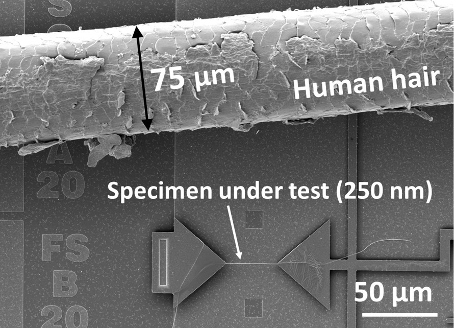
Figure 8.
SEM image of a 250 nm diameter NF in comparison with human hair. Inset: detailed view of gripped nanofiber.
Figure 8.
SEM image of a 250 nm diameter NF in comparison with human hair. Inset: detailed view of gripped nanofiber.

Figure 9.
Schematic diagrams representing nanofiber placement onto a platinum resistance thermometer plates. (a) suspended plates, (b) a small drop of isopropanol (IPA) is placed on the platforms (c) after the IPA evaporates, the microheater cuts the fibers, (d) The evaporating IPA pulls the fiber into contact with the plate.

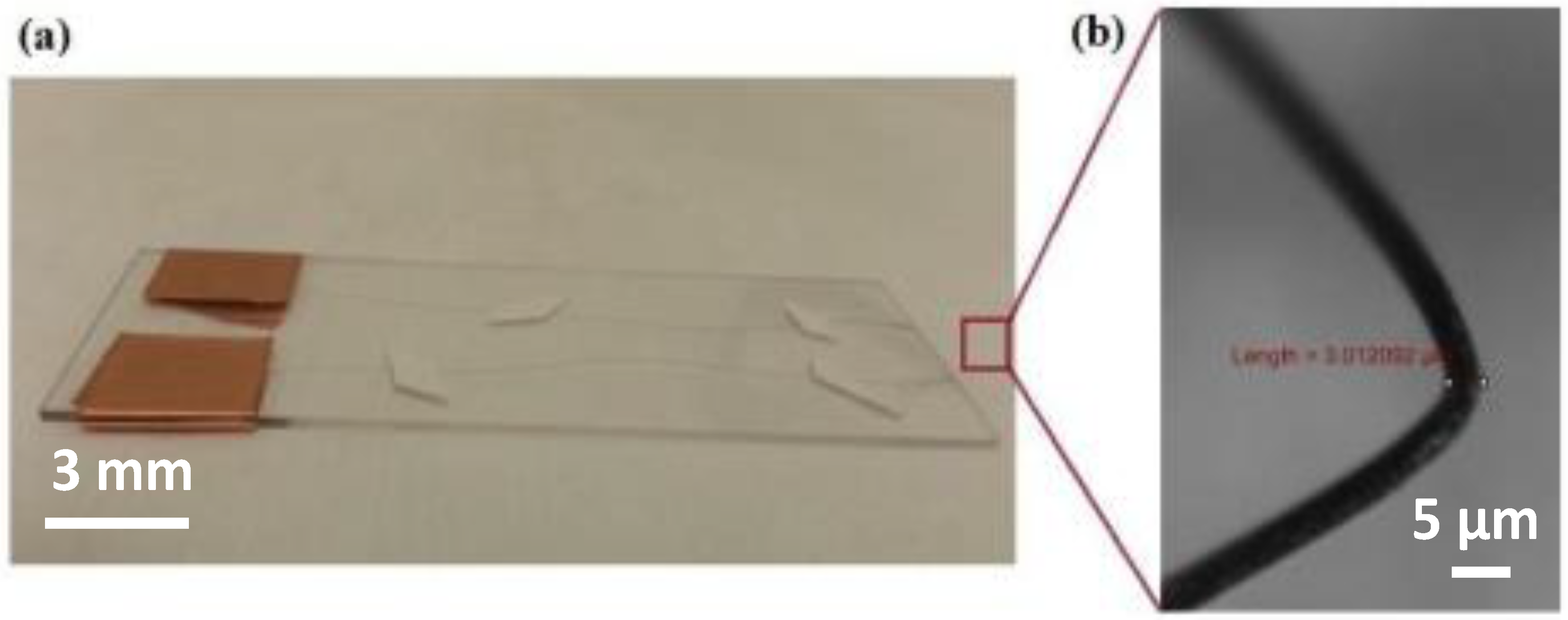
Figure 10.
Optical image of a UHWMPE nanofiber sample mounted on the thermal device.

Figure 11.
Stress–strain curves for the silica nanofibers.

Figure 12.
Estimate of glue shear strength. (a) Shear force per unit length versus fiber diameter for Loctite® AA 3032/Henkel glue/fiber interface. The slope gives the shear strength of the glue/nanofiber interface. (b,c) are schematic cross-section and longitudinal views of the fiber in the glue. Adapted from reference [3] supplementary information.

Figure 13.
(a) NF attached by a platinum coating using FIB. (b) The thermal conductivity values of NF prepared by this procedure are similar to bulk PE due to the damage in the NF chains. Adapted from reference [3] supplementary information.
Figure 13.
(a) NF attached by a platinum coating using FIB. (b) The thermal conductivity values of NF prepared by this procedure are similar to bulk PE due to the damage in the NF chains. Adapted from reference [3] supplementary information.

© 2018 by the authors. Licensee MDPI, Basel, Switzerland. This article is an open access article distributed under the terms and conditions of the Creative Commons Attribution (CC BY) license (http://creativecommons.org/licenses/by/4.0/).
Share and Cite
MDPI and ACS Style
Shrestha, R.; Shen, S.; P. de Boer, M. Preparing and Mounting Polymer Nanofibers onto Microscale Test Platforms. Actuators 2018, 7, 71. https://doi.org/10.3390/act7040071
AMA Style
Shrestha R, Shen S, P. de Boer M. Preparing and Mounting Polymer Nanofibers onto Microscale Test Platforms. Actuators. 2018; 7(4):71. https://doi.org/10.3390/act7040071
Chicago/Turabian StyleShrestha, Ramesh, Sheng Shen, and Maarten P. de Boer. 2018. "Preparing and Mounting Polymer Nanofibers onto Microscale Test Platforms" Actuators 7, no. 4: 71. https://doi.org/10.3390/act7040071
Note that from the first issue of 2016, this journal uses article numbers instead of page numbers. See further details here.