Article

Optimization of Fluorine Plasma Treatment for Interface Improvement on HfO2/In0.53Ga0.47As MOSFETs

Microelectronics Research Center, Department of Electrical and Computer Engineering, The University of Texas at Austin, TX 78758, USA
*
Author to whom correspondence should be addressed.
Appl. Sci. 2012, 2(1), 233-244; https://doi.org/10.3390/app2010233
Submission received: 30 January 2012 / Revised: 20 February 2012 / Accepted: 10 March 2012 / Published: 19 March 2012
(This article belongs to the Special Issue Organo-Fluorine Chemical Science)

Abstract

:
This paper reports significant improvements in the electrical performance of In0.53Ga0.47As metal-oxide-semiconductor field-effect transistors (MOSFET) by a post-gate CF4/O2 plasma treatment. The optimum condition of CF4/O2 plasma treatment has been systematically studied and found to be 30 W for 3–5 min. Approximately 5× reduction in interface trap density from 2.8 × 10¹² to 4.9 × 1011 cm−2eV−1 has been demonstrated with fluorine (F) incorporation. Subthreshold swing has been improved from 127 to 109 mV/dec. Effective channel mobility has been enhanced from 826 to 1,144 cm2/Vs.

Graphical Abstract

1. Introduction

In0.53Ga0.47As based-III-V compounds have attracted a great deal of attention for their advantages in high electron mobility over their Si-based counterparts. However, poor interface quality between In0.53Ga0.47As and high dielectric constant (high-k) gate dielectrics has imposed an enormous challenge for implementing inversion-type enhancement mode metal-oxide-semiconductor field-effect transistors (MOSFETs). Proper surface pre-treatment and insertion of interface passivation layer [1,2,3] have generally employed to achieve improved interface quality. Those approaches usually performed prior to high-k deposition, however, interface state traps created during the high-k deposition need to be passivated by a post-oxide treatment.
It can be expected that fluorine (F) will be an effective passivation agent for In0.53Ga0.47As because F has high binding energy with In (5.25 eV), Ga (5.99 eV), and As (4.26 eV), respectively [4]. F incorporation has been demonstrated on Si, Ge, and In0.53Ga0.47As substrates. It has been found that F can passivate high-k bulk traps and interface defects at high-k/substrates (Si, Ge and In0.53Ga0.47As) interface [5,6,7,8,9]. Although previous reports showed that the insertion of a thin interface passivation layer could improve interface quality [10], those layers usually have relative lower k value [11]. This may hinder equivalent oxide thickness (EOT) scaling and as a result, hardly meet the requirement for the sub 22 nm nodes.
In this paper, we systematically studied the effects of CF4/O2 plasma power wattage and treatment time on HfO2/In0.53Ga0.47As gate stack. The condition of CF4/O2 plasma has been optimized, which significantly improves the effective channel mobility (µeff), transconductance (Gm), drive current (Id), and subthreshold swing (SS). With F incorporation, we have successfully developed excellent interface quality of HfO2 directly on In0.53Ga0.47As without using interface passivation layer. Fluorinated samples exhibit low interface trap density (Dit) of 4.9 × 1011 cm−2eV−1, which is the lowest value compared to prior reported HfO2/In0.53Ga0.47As gate stacks.

2. Experimental Section

Figure 1 shows the device structure and the illustration of F incorporation. The wafers used in our study were molecular beam epitaxy grown by a vender. P-type (Zn-doped, 3 × 10¹⁸/cm3) InP wafers were the starting substrates. P-type (Be-doped, 5 × 10¹⁶/cm3) In0.52Al0.48As of 100 nm thick was grown as a buffer layer, followed by a 300 nm p-type In0.53Ga0.47As layer (Be-doped, 5 × 10¹⁶/cm3), which was used as the channel layer. The native oxides were removed with 1% diluted HF solution, followed by 20% (NH4)2S solution for sulfur passivation. To protect gate stack from the source and drain (S/D) activation annealing, the gate-last process was adopted: A 10-nm-thick atomic-layer-deposited (ALD) Al2O3 was deposited at a substrate temperature of 200 °C as an encapsulation layer. S/D regions were selectively implanted with a Si dose of 2 × 10¹⁴/cm2 at 35 keV. The S/D activation annealing was performed in nitrogen ambient at 700 °C/10 s. The encapsulation layer was then removed using buffered oxide etch solution. A 5 nm-thick ALD HfO2 film was deposited after the same surface preparation (HF and (NH4)2S). Some samples were treated ex situ with CF4 plasma with varied RF wattages and treatment times. A mixed flow of CF4 and O2 gas (ratio ~10:1) was introduced into the chamber with pressure of 100 mTorr. The purpose of O2 flow was to avoid carbon contamination. Control samples without CF4/O2 plasma treatment were also fabricated as references. Post-deposition annealing was then performed for all the samples at 500 °C for 60 s in a nitrogen ambient. Subsequently, a 200 nm TaN was sputtered and patterned as gate electrode. AuGe/Ni/Au alloy was deposited by E-beam evaporation and a liftoff process to form S/D Ohmic contacts; backside contact was made by E-beam evaporation of Cr/Au, followed by annealing at 400 °C for 30 s in nitrogen ambient.
Figure 1. The device cross-sectional structure of HfO2/In0.53Ga0.47As gate stack. Samples were treated in a mixed flow of CF4 and O2 gas (ratio ~10:1) with varied RF power and treatment time.
Applsci 02 00233 g001
Figures 2 and 3 show the X-ray photoelectron spectroscopy (XPS) spectra of Hf 4f and F 1s for the HfO2/In0.53Ga0.47As gate stack with and without CF4/O2 plasma treatment. All the scanned binding energy was calibrated by the C 1s signal at 284.5 eV.
Figure 2. X-ray photoelectron spectroscopy (XPS) analysis of the Hf 4f electronic spectra for the samples with and without fluorine (F) incorporation.
Applsci 02 00233 g002
Figure 3. XPS analysis of the F 1s electronic spectra for the control sample and fluorinated sample.
Applsci 02 00233 g003
Compared to the control sample, the fluorinated sample has an increased binding energy by 0.2 eV and 0.3 eV for the Hf 4f7/2 and Hf 4f5/2 signal, respectively. This suggests that parts of the oxygen vacancies were terminated by the incorporated F atoms to form stronger Hf-F bonds with higher binding energy. In Figure 3, the peak signal located at ~685 eV corresponds to the F bonds in the bulk HfO2, indicating that F was incorporated into the HfO2 after CF4/O2 plasma treatment.
In order to search the F distribution in the HfO2/In0.53Ga0.47As gate stack, the secondary ion mass spectrometry (SIMS) technique was examined, as shown in Figure 4. A considerable amount of F was incorporated into the HfO2 gate stacks with CF4/O2 plasma treatment while the oxygen concentration remained similar. Due to sudden structural transition at the HfO2/In0.53Ga0.47As interface, the density of defective bonds at the interface is much higher than that in the HfO2 bulk. F tends to pile up at the HfO2/In0.53Ga0.47As interface passivating interface traps, resulting in a better interface quality (discussed later in this paper).
Figure 4. Secondary ion mass spectrometry (SIMS) profile of elements in the HfO2/In0.53Ga0.47As gate stack with and without CF4/O2 plasma treatment. The CF4/O2 plasma condition is 30 W for 3 min.
Applsci 02 00233 g004
The composition and stoichiometry of HfO2 were determined by XPS analysis (data not shown). For the control sample, HfO2 was in good stoichiometry (Hf:O = 1:2) and it became oxygen-rich (HfO2.25) after CF4/O2 plasma treatment. One possibility of improvements could be due to the oxygen vacancies passivation during the plasma treatment. The effect of O2 plasma treatment is under investigation.
One concern of doping F into gate oxide is that dielectric constant of the gate oxide would decrease with heavy F incorporation. From XPS, the F concentration in our fluorinated HfO2 is estimated to be 2.7 at.%, which is lower than that used in the low-k technology [12]. Therefore, the dielectric constant of HfO2 remains similar (~17) after F incorporation, as shown in Figure 5. The inset of Figure 5 compares the gate leakage current of samples with and without F incorporation. The gate leakage current is slightly reduced with F incorporation.
Figure 5. Equivalent oxide thickness (EOT) versus physical thickness for the samples with and without F incorporation. Inset: the gate leakage current comparison of samples with and without F incorporation.
Applsci 02 00233 g005
One objective of this work is to investigate the optimum condition of CF4/O2 plasma. The RF power and the plasma treatment time are two critical factors that affect the electrical characteristics significantly. Insufficient plasma treatment might not improve the gate dielectric quality, whereas excessive plasma treatment possibly causes plasma damage and corrodes the improvement. To study the effects of RF power on HfO2 gate dielectrics, some samples were treated in CF4/O2 plasma for 3 min at different RF power in the range from 20 to 40 W. It was found that the samples treated by the power of 30 W improved most in terms of Gm, Id and SS. With the fixed RF power of 30 W, we continued to study the effect of CF4/O2 plasma treatment time. Some samples were treated in CF4/O2 plasma at different treatment times ranging from 1 to 7 min with a fixed RF power of 30 W. It was found that 5 min plasma treatment further improved SS.

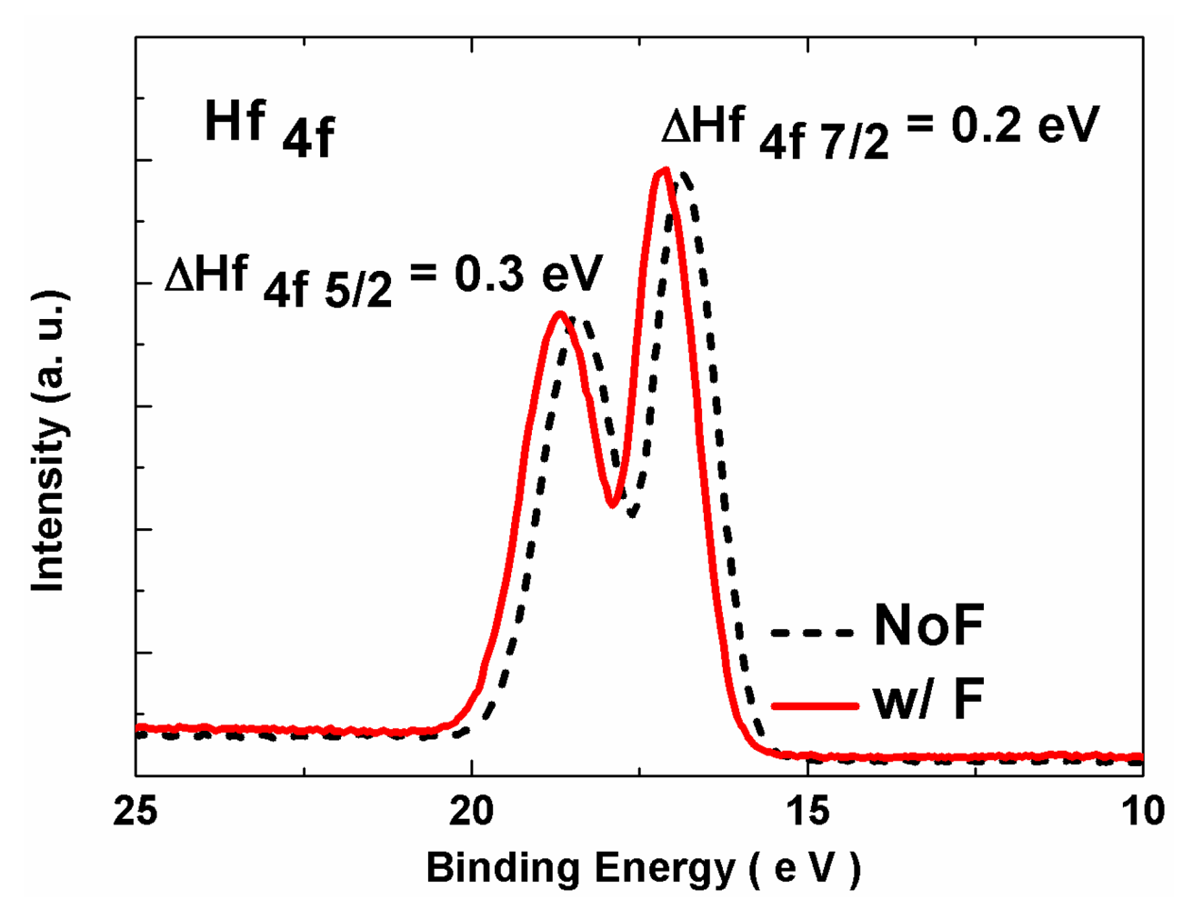
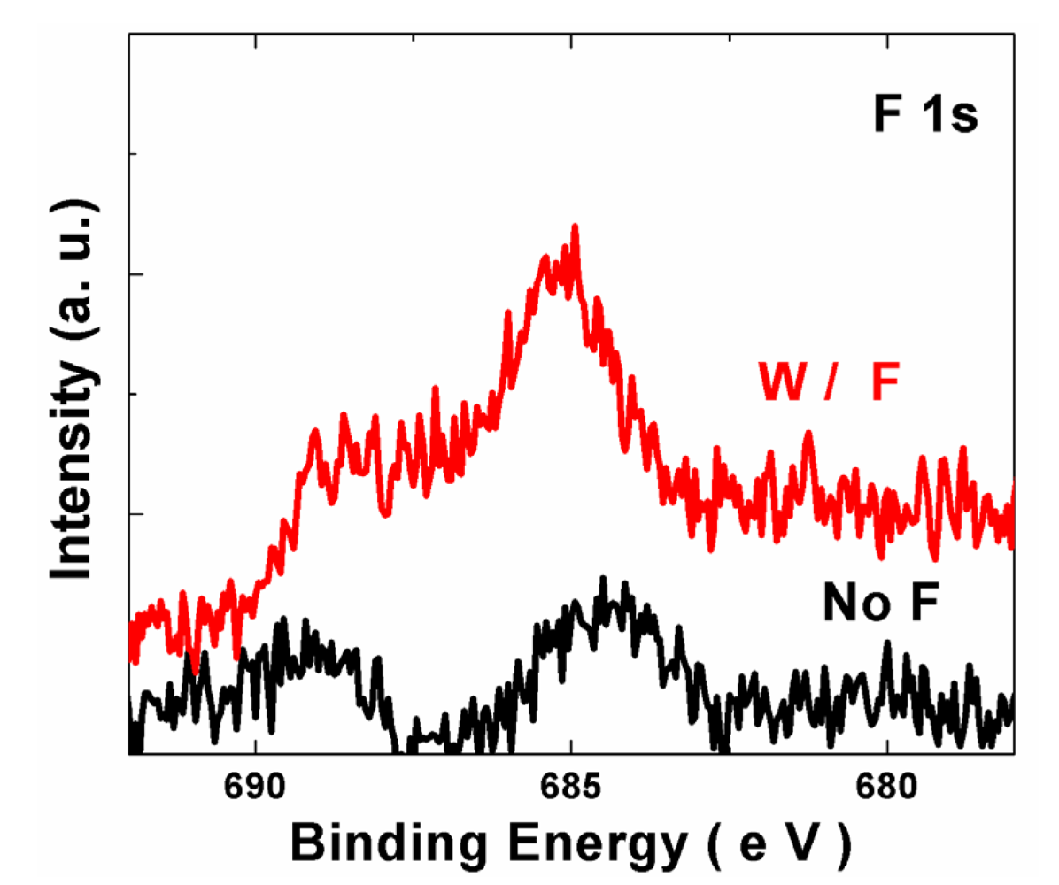
3. Results and Discussion

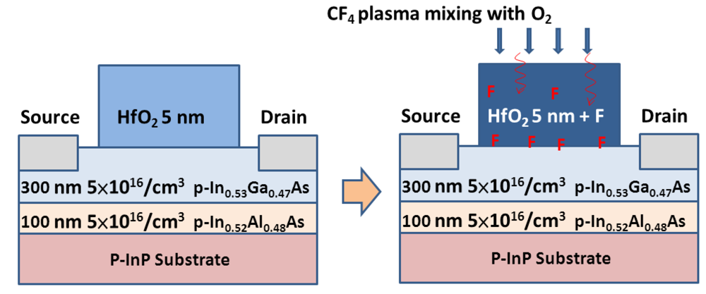
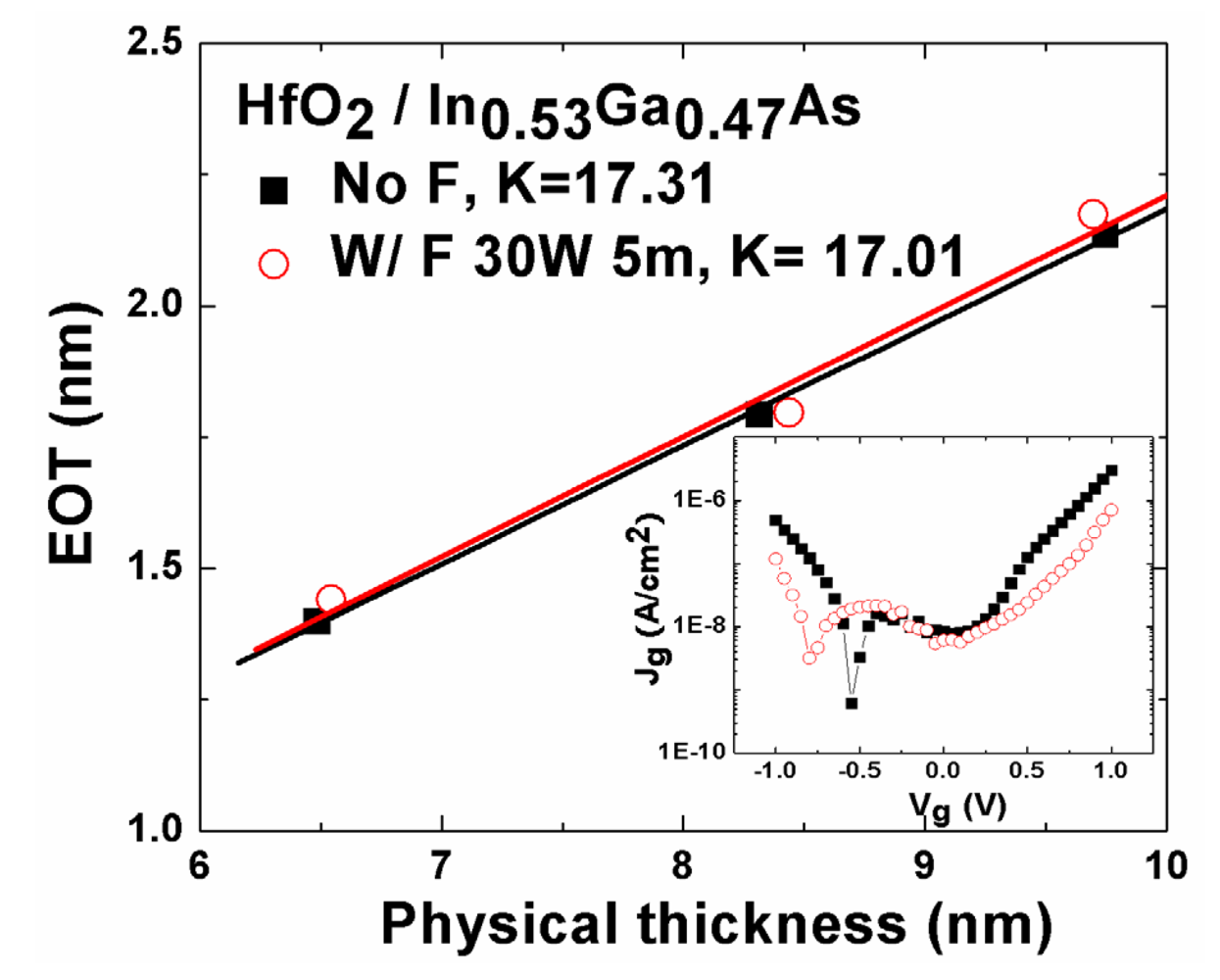
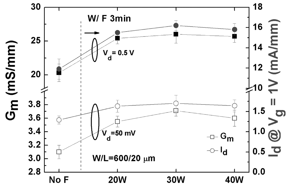
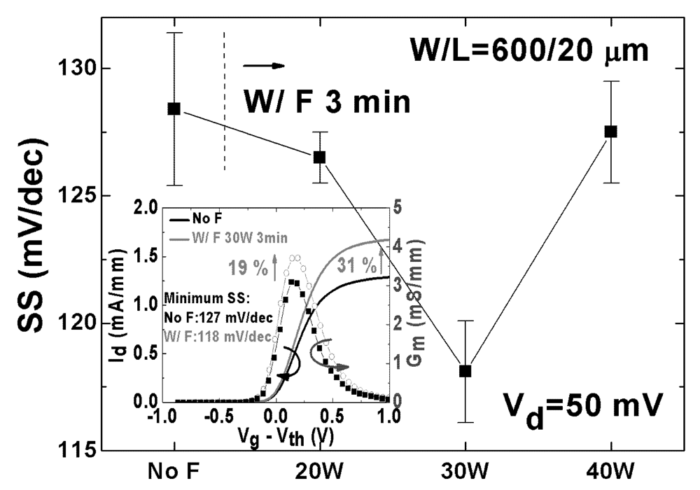
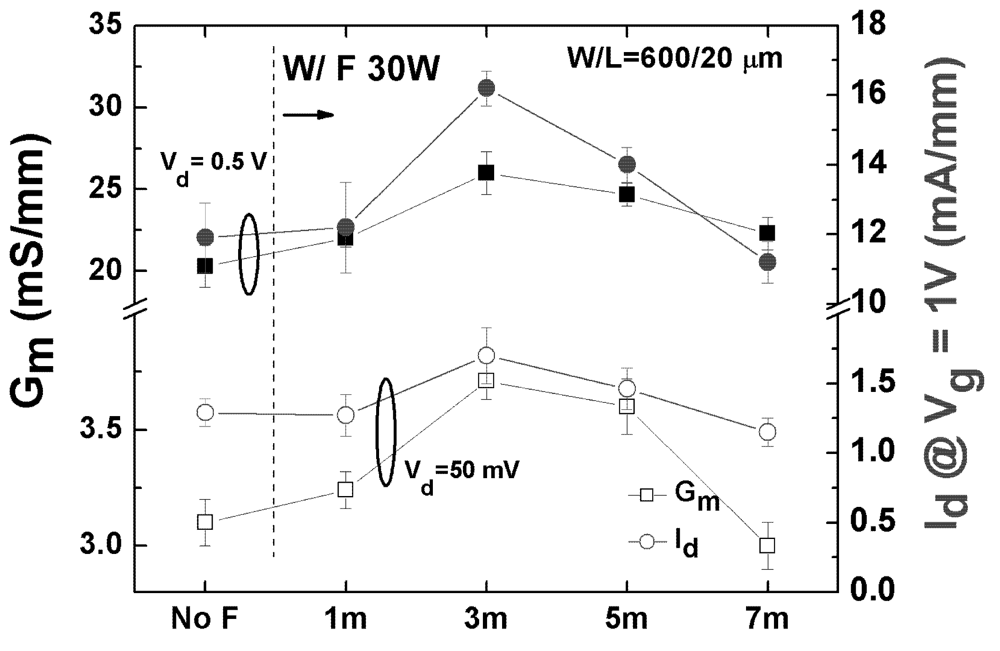
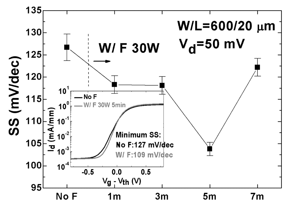
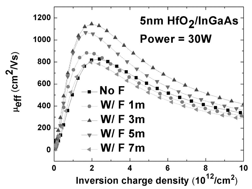
3.1. Optimization of CF4/O2 Plasma

The maximum Gm and Id as a function of different RF power (CF4/O2 plasma treatment time: 3 min) are shown in Figure 6 (W/L = 600/20 µm, at Vd = 50 mV and 0.5 V). The maximum Gm and Id of the control sample are 3.1 mS/mm and 1.3 mA/mm (Vd = 50 mV), and 20.3 mS/mm and 12 mA/mm (Vd = 0.5 V), respectively. With F plasma treatment of 30W, the maximum Gm and Id reach 3.7 mS/mm and 1.7 mA/mm (Vd = 50 mV), and 26 mS/mm and 16.2 mA/mm (Vd = 0.5 V), respectively. However, the maximum Gm and Id roll back with power larger than 30 W indicative of possible plasma damage. SS data with different RF power are shown in Figure 7. In0.53Ga0.47As MOSFETs have similar EOT (~1.4 nm, data not shown) with different RF power treatment. With F incorporation, SS has been improved from 127 to 118.1 mV/dec (as shown in the inset of Figure 7), which suggests that the interface quality has been improved. For the RF power of 40W, SS increases to 127.5 mV/dec, indicating that excessive CF4/O2 plasma treatment degrades the interface quality.
Figure 6. Maximum Gm and Id as a function of CF4/O2 plasma RF power (W/L = 600 µm/20 µm at Vd = 50 mV and 0.5 V). CF4/O2 plasma treatment time: 3 min.
Applsci 02 00233 g006
Figure 7. Subthreshold swing (SS) as a function of CF4/O2 plasma RF power. CF4/O2 plasma treatment time: 3 min. Inset: Id-Vg comparison of the control sample and the sample with CF4/O2 plasma treatment for 30W/3min.
Applsci 02 00233 g007
Figure 8 compares the maximum Gm and Id as a function of plasma treatment times ranging from 1 to 7 min with a fixed RF power of 30W (W/L = 600 µm/20 µm at Vd = 50 mV and 0.5 V). 3 min plasma treatment reaches the peak values of the maximum Gm and Id, whereas 5 min plasma treatment achieves the lowest SS value (Figure 9). The inset of Figure 8 compares the Id-Vg curves (in log-linear scale) of the control sample and the sample with F treatment 30 W/5 min. A steeper SS slope is clearly observed.
Figure 8. Maximum Gm and Id as a function of CF4/O2 plasma treatment time (W/L = 600 µm/20 µm at Vd = 50 mV and 0.5 V). RF power: 30 W.
Applsci 02 00233 g008
Figure 9. SS as a function of CF4/O2 plasma treatment time. RF power: 30 W. Inset: Id-Vg comparison of the control sample and the sample with CF4 plasma treatment for 30 W/5 min.
Applsci 02 00233 g009
Effective channel mobility (µeff) of In0.53Ga0.47As MOSFETs with different plasma treatment times are plotted in Figure 10. The peak µeff of 30 W/3 min reaches 1,144 cm2/Vs, which is 38% improvement compared to the control samples (826 cm2/Vs). The improvements in the Id, Gm, SS and µeff are believed to be due to the improved interface quality by an appropriate amount of CF4/O2 plasma post-HfO2 treatment.
Figure 10. Effective channel mobility versus inversion charge density as a function of CF4/O2 plasma treatment time. RF power: 30 W.
Applsci 02 00233 g010
We noticed that the plasma damage occurred if excessive plasma (either plasma wattage or treatment time) was applied. The plasma damage could come from disordering, surface roughening, and fluorine contamination [13]. The disordering layer contains dangling bonds and broken bonds, which would scatter the electrons underneath (in the channel) and lower the electron mobility. Severe disordering would lead to surface roughness, which results in more dangling bonds and broken bonds. If the F concentration is too high (>5 at.%, [12]), the dielectric constant of HfO2 decreases, resulting in lowering drive current.

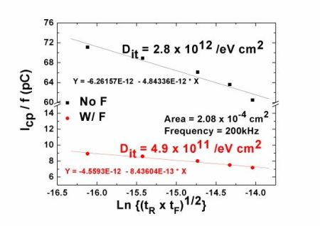
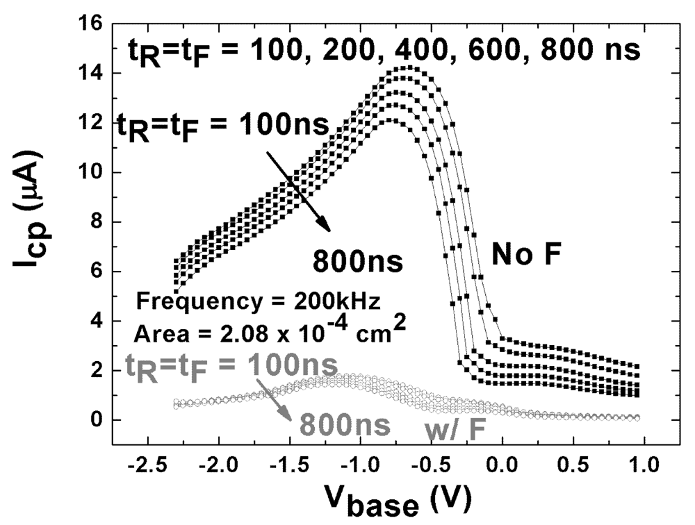
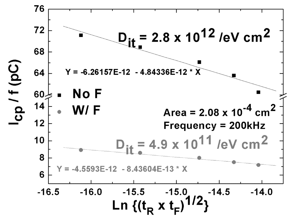
3.2. Electrical Characterization of the Interface Trap Density

Charge pumping measurements were conducted to accurately evaluate the interface quality of the control and fluorinated MOSFETs. The charge pumping characterization was performed by sweeping the base level voltage (Vbase, −2.3 V to 1 V in a step of 50 mV) of the trapezoidal gate pulse (with a constant-amplitude, 1 V) at 200 KHz. The S/D terminals were grounded. The region of the bandgap probed was from electron emission energy level to hole emission energy level, which was around the midgap. The charge pumping current (Icp) is plotted as a function of Vbase for equal trapezoidal pulse rise time (tR) and fall time (tF), as shown in Figure 11. tR and tF are varied from 100 to 800 ns. Lower Icp for the fluorinated sample is indicative of reduced Dit. The mean Dit value can be extracted according to the following equation [14,15],
Applsci 02 00233 i001
where q is the electronic charge, A is the transistor gate area (2.08 × 10⁻⁴ cm2 in our devices), k is the Boltzmann constant, Vfb is the flat band voltage, Vt is the threshold voltage, ∆Vg is the gate pulse amplitude, Vth is the thermal velocity of the carriers, ni is the surface concentration of minority carriers, and σn and σp are the capture cross sections of electrons and holes, respectively. The mean Dit values were extracted from the slope of Icp/fversus ln[(tR × tF)1/2], as shown in Figure 12. It has been found that the mean Dit value was reduced ~5× from 2.8 × 10¹² to 4.9 × 1011 cm−2eV−1 after F plasma treatment. F atoms possibly passivate dangling bonds and oxygen vacancies in the HfO2/In0.53Ga0.47As interface and thereby reduce Dit value.
Figure 11. Charge pumping measurement with rise/fall time dependence. Samples with F incorporation show much smaller Icp. Vbase: −2.3 V to 1 V in a step of 50 mV and the pulse amplitude is 1 V.
Applsci 02 00233 g011
Figure 12. Qcp (=Icp/f) vs. ln[(tR × tF)1/2]. The mean Dit value is extracted by linear fitting according to References [14,15]. Samples with F incorporation show less Dit value of 4.9 × 10¹¹/eVcm2.
Applsci 02 00233 g012
Table 1 compares the device performance and interfacial properties of In0.53Ga0.47As MOSFETs reported in this paper and other high-k/In0.53Ga0.47As gate stacks in recent publications. The Dit value reported in this paper is the lowest value compared to prior reported HfO2/In0.53Ga0.47As gate stacks.
Table 1. Comparison of the electrical and interfacial properties of this work with some recently reported paper.
High kPassivation methodChannel materialLGEOT or thickness of high-kDitSS (mV/dec)Ref.
(cm−2eV1)
Al2O3 *-In0.53Ga0.47As-4.2 nm5 × 1011-[16]
Al2O3-In0.53Ga0.47As-10 nm of Al2O32.5 × 1011-[17]
Al2O3-In0.53Ga0.47As1.5 µm8 nm of Al2O31 × 1012>200[18]
Al2O3-In0.53Ga0.47As0.5 µm30 nm of Al2O31.4 × 1012240[19]
HfO2 *-In0.53Ga0.47As-2.1 nm1 × 1012-[16]
HfO2 *-In0.53Ga0.47As-7.8 nm of HfO22 × 1012-[20]
HfO2 *Al-dopedIn0.53Ga0.47As-8–9 nm of HfO26 × 1012-[21]
HfO2 *PH3In0.53Ga0.47As4 µm1.7 nm8.6 × 1011103[22]
HfAlOSiH4+NH3In0.53Ga0.47As2–10 µm3.8 nm6.5 × 1011155–210[2]
ZrO2LaAlO3In0.53Ga0.47As5 µm1.63 nm7.5 × 1011116[23]
HfO2CF4/O2 post treatmentIn0.53Ga0.47As5–20 µm1.4 nm4.9 × 1011109This work
HfO2Control1.35 nm2.8 × 1012127This work
* Capacitor structure.

4. Conclusions

The effects of post-oxide CF4/O2 treatment on HfO2/In0.53Ga0.47As gate stack have been systematically investigated. The condition for the CF4/O2 plasma is optimized to be 30 W for 3-5 min. The gate stack interface quality has been notably improved by F incorporation. The mean Dit value has been reduced ~5× from 2.8 × 10¹² to 4.9 × 1011 cm−2eV−1. As a result, enhanced electrical performances have been presented: steeper SS from 127 to 109 mV/dec, enhanced µeff from 826 to 1,144 cm2/Vs, and improved Gm and Id from 3.1 to 3.7 mS/mm and from 1.3 to 1.7 mA/mm, respectively (at Vd = 50 mV, 20 µm channel length). These results suggest that the post-HfO2 F treatment could be a key technique to implement high performance III-V MOSFETs for the sub 22 nm nodes.

References

  1. Shahrjerdi, D.; Tutuc, E.; Banerjee, S.K. Impact of surface chemical treatment on capacitance-voltage characteristics of GaAs metal-oxide-semiconductor capacitors with Al2O3 gate dielectric. Appl. Phys. Lett. 2007, 91, 063501. [Google Scholar]
  2. Chin, H.-C.; Liu, X.; Gong, X.; Yeo, Y.-C. Silane and ammonia surface passivation technology for high-mobility In0.53Ga0.47As MOSFETs. Trans. Electron. Devices 2010, 57, 973–979. [Google Scholar]
  3. Chen, Y.-T.; Zhao, H.; Yum, J.H.; Wang, Y.; Lee, J.C. Metal-oxide-semiconductor field-effect-transistors on indium phosphide using HfO2 and silicon passivation layer with equivalent oxide thickness of 18 Å. Appl. Phys. Lett. 2009, 94, 213505. [Google Scholar]
  4. CRC, Handbook of Physics and Chemistry, 84 ed; CRC: Boca Raton, FL, USA, 2003.
  5. Wu, W.-C.; Lai, C.-S.; Lee, S.-C.; Ma, M.-W.; Chao, T.-S.; Wang, J.-C.; Hsu, C.-W.; Chou, P.-C.; Chen, J.-H.; Kao, K.-H.; et al. Fluorinated HfO2 Gate Dielectrics Engineering for CMOS by Pre- and Post-CF4 Plasma Passivation. In Proceedings of IEEE International Electron Devices Meeting, San Francisco, CA, USA, 15-17 December 2008; pp. 1–4.
  6. Seo, K.; Sreenivasan, R.; McIntyre, P.C.; Saraswat, K.C. Improvement in high-k (HfO2/SiO2) reliability by incorporation of fluorine. IEEE Electron. Device Lett. 2006, 27, 821–823. [Google Scholar] [CrossRef]
  7. Xie, R.; He, W.; Yu, M.; Zhu, C. Effects of fluorine incorporation and forming gas annealing on high-k gated germanium metal-oxide-semiconductor with GeO2 surface passivation. Appl. Phys. Lett. 2008, 93, 073504. [Google Scholar] [CrossRef]
  8. Chin, H.-C.; Gong, X.; Wang, L.; Yeo, Y.-C. Fluorine incorporation in HfAlO gate dielectric for defect passivation and effect on electrical characteristics of In0.53Ga0.47As n-MOSFETs. Electrochem. Solid State Lett. 2010, 13, H440–H442. [Google Scholar]
  9. Chen, Y.-T.; Zhao, H.; Yum, J.H.; Wang, Y.; Xue, F.; Zhou, F.; Lee, J.C. Improved electrical characteristics of TaN/Al2O3/In0.53Ga0.47As metal-oxide-semiconductor field-effect transistors by fluorine incorporation. Appl. Phys. Lett. 2009, 95, 013501. [Google Scholar]
  10. Zhao, H.; Chen, Y.; Yum, J.H.; Wang, Y.; Lee, J.C. HfO2-based In0.53Ga0.47As MOSFETs (EOT ≈ 10Å) Using Various Interfacial Dielectric Layers. In Proceedings of IEEE 67th Device Research Conference, University Park, PA, USA, 22-24 June 2009; pp. 89–90.
  11. Zhao, H.; Yum, J.H.; Chen, Y.-T.; Lee, J.C. In0.53Ga0.47As n-metal-oxide-semiconductor field effect transistors with atomic layer deposited Al2O3, HfO2, and LaAlO3 gate dielectrics. J. Vac. Sci. Technol. B 2009, 27, 2024–2027. [Google Scholar] [CrossRef]
  12. Lee, S.; Park, J.-W. Effect of fluorine on dielectric properties of SiOF films. J. Appl. Phys. 1996, 80, 5260–5263. [Google Scholar]
  13. Tatsumi, T.; Fukuda, S.; Kadomura, S. Etch rate acceleration of SiO2 during wet treatment after gate etching. Jpn. J. Appl. Phys. 1993, 32, 6114–6118. [Google Scholar]
  14. Groeseneken, G.; Maes, H.E.; Beltran, N.; Dekeersmaecker, R.F. A reliable approach to charge-pumping measurements in MOS transistors. IEEE Trans. Electron. Devices 1984, 31, 42–53. [Google Scholar] [CrossRef]
  15. Xie, R.; Phung, T.H.; He, W.; Sun, Z.; Yu, M.; Cheng, Z.; Zhu, C. High Mobility High-k/Ge pMOSFETs with 1 nm EOT—New Concept on Interface Engineering and Interface Characterization. In Proceedings of 2008 IEEE International Electron Devices Meeting (IEDM), San Francisco, CA, USA, 15-17 December 2008; pp. 393–396.
  16. Zhao, H.; Huang, J.; Chen, Y.-T.; Yum, J.H.; Wang, Y.; Xue, F.; Zhou, F.; Lee, J.C. Effects of gate-first and gate-last process on interface quality of In0.53Ga0.47As metal-oxide-semiconductor capacitors using atomic-layer-deposited Al2O3 and HfO2 oxides. Appl. Phys. Lett. 2009, 95, 253501. [Google Scholar]
  17. Chiu, H.C.; Tung, L.T.; Chang, Y.H.; Lee, Y.J.; Chang, C.C.; Kwo, J.; Hong, M. Achieving a low interfacial density of states in atomic layer deposited Al2O3 on In0.53Ga0.47As. 53Ga0.47As. Appl. Phys. Lett. 2008, 93, 202903. [Google Scholar]
  18. Lin, D.; Brammertz, G.; Sioncke, S.; Fleischmann, C.; Delabie, A.; Martens, K.; Bender, H.; Conard, T.; Tseng, W.H.; Lin, J.C.; et al. Enabling the high-performance InGaAs/Ge CMOS: A common gate stack solution. In Proceedings of 2009 IEEE International Electron Devices Meeting (IEDM), Baltimore, MD, USA, 7-9 December 2009; pp. 1–4.
  19. Xuan, Y.; Wu, Y.; Shen, T.; Yang, T.; Ye, P. High Performance Submicron Inversion-Type Enhancement-Mode InGaAs MOSFETs with ALD Al2O3,HfO2 and HfAlO as Gate Dielectrics. In Proceedings of 2007 IEEE International Electron Devices Meeting (IEDM), Washington, DC, USA, 10-12 December 2007; pp. 637–640.
  20. Chang, Y.C.; Huang, M.L.; Lee, K.Y.; Lee, Y.J.; Lin, T.D.; Hong, M.; Kwo, J.; Lay, T.S.; Liao, C.C.; Cheng, K.Y. Atomic-layer-deposited HfO2 on In0.53Ga0.47As: Passivation and energy-band parameters. Appl. Phys. Lett. 2008, 92, 072901. [Google Scholar]
  21. Hwang, Y.; Chobpattana, V.; Zhang, J.Y.; LeBeau, J.M.; Engel-Herbert, R.; Stemmer, S. Al-doped HfO2/In0.53Ga0.47As metal-oxide-semiconductor capacitors. Appl. Phys. Lett. 2011, 98, 142901. [Google Scholar]
  22. Lin, J.; Lee, S.; Oh, H.-J.; Yang, W.; Lo, G.Q.; Kwong, D.L.; Chi, D.Z. Plasma PH3-Passivated High Mobility Inversion InGaAs MOSFET Fabricated with Self-Aligned Gate-First Process and HfO2/TaN Gates Stack. In Proceedings of 2008 IEEE International Electron Devices Meeting (IEDM), San Francisco, CA, USA, 15-17 December 2008; pp. 401–404.
  23. Huang, J.; Goel, N.; Zhao, H.; Kang, C.Y.; Min, K.S.; Bersuker, G.; Oktyabrsky, S.; Gaspe, C.K.; Santos, M.B.; Majhi, P.; et al. InGaAs MOSFET Performance and Reliability Improvement by Simultaneous Reduction of Oxide and Interface Charge in ALD (La)AlOx/ZrO2 Gate Stack. In Proceedings of 2009 IEEE International Electron Devices Meeting (IEDM), Baltimore, MD, USA, 7-9 December 2009; pp. 335–338.

