Article

Electro-Physical Interpretation of the Degradation of the Fill Factor of Silicon Heterojunction Solar Cells Due to Incomplete Hole Collection at the a-Si:H/c-Si Thermionic Emission Barrier

by
Moustafa Ghannam
* and
Yaser Abdulraheem
College of Engineering and Petroleum, Kuwait University, 13060 Safat, Kuwait
*
Author to whom correspondence should be addressed.
Appl. Sci. 2018, 8(10), 1846; https://doi.org/10.3390/app8101846
Submission received: 23 July 2018 / Revised: 12 September 2018 / Accepted: 20 September 2018 / Published: 8 October 2018
(This article belongs to the Special Issue Next Generation Photovoltaic Solar Cells)

Abstract

:
An electro-physical interpretation for the degradation of the Fill Factor in p+/n silicon heterojunction solar cells (SHJ) due to incomplete hole collection at the thermionic emission barrier at the amorphous/crystalline silicon (a-Si:H/c-Si) hetero-interface is proposed supported by results of AFORS-HET device simulations. Under illumination, reflected holes at the thermionic barrier pile up at the hetero-interface which strengthens the dipole with the negative dopant ions in the doped a-Si:H(p+) layer and enhances the electric field passing through the a-Si:H layer. Such an enhanced electric field sweeps back the free holes spilling over in the intrinsic a-Si:H(i) layer from the a-Si:H(p+) layer considerably depleting the double a-Si:H layer and enhancing its resistance and the overall cell series resistance. Therefore, the degradation due to incomplete hole collection at the thermionic emission barrier under illumination can be assimilated to the effect of a series resistance does not affect the cell open circuit voltage but degrades only its fill factor. The resistance enhancement is found to be bias-dependent and to increase with decreasing the doping level in a-Si:H(p+). Predictions of the proposed model for different hole reflection probability at the barrier and for different thicknesses of the intrinsic a-Si:H(i) layer agree perfectly with the results of simulations.

1. Introduction

The carrier selection property of the amorphous/crystalline silicon (a-Si:H/c-Si) hetero-junction has been demonstrated for the first time more than three decades ago on npn bipolar junction transistors, which showed enhanced a-Si:H emitter efficiency and current gain [1,2]. Such a property has then been exploited later to reduce the dark current and increase the open circuit voltage (VOC) of the a-Si:H/c-Si heterojunction solar (SHJ) cell [3,4]. Extensive research and development have been devoted to the design and technology of such a cell, especially p+ doped a-Si:H(p+) on n-type c-Si substrate, which led to a continuous improvement in the cell efficiency [5,6] to presently exceed 26% [7].
The superior performance of the SHJ cell is mainly the result of the reduced saturation current of the p-type inversion layer emitter induced in the n-type c-Si side of the a-Si:H/c-Si hetero-interface [8,9]. This results in a strong boost in VOC to reach values close to 760 mV, which cannot be achieved in any other type of high efficiency c-Si cell. Several factors contribute to minimizing the emitter dark saturation current and hence to the VOC boost in the SHJ cell. Minimum interface recombination is ensured by inserting an ultrathin intrinsic a-Si:H(i) buffer layer between the a-Si:H(p+) layer and the c-Si substrate [3,4]. In addition, band-gap narrowing in the heavily populated inversion layer is expected to be less significant than in doped layers. Band-gap widening has even been reported in strong inversion layers due to carrier quantum confinement [10,11], which results in a much smaller intrinsic carrier concentration in the p+ inversion layer compared to heavily doped emitters. Finally, bulk recombination in the very thin inversion layer emitter is expected to be negligible. All these factors are usually lumped in the statement: “excellent passivation property of the a-Si:H contact” commonly used to justify the very small emitter saturation current of SHJ cells. It has been shown that the stronger the inversion, the better the cell performance [8], which means that the equilibrium band bending at the hetero-interface and consequently the difference between the work function of a-Si:H and that of c-Si should be large. Therefore, maximum free hole concentration in the p-type doped a-Si:H(p+) layer should be ensured. On the other hand, low a-Si:H doping levels or significant depletion of the layer results in a weak inversion layer with degraded cell performance [8,12]. It has also been shown that using non-appropriate material with a relatively small work function for the Transparent Conducting Oxide (TCO) used at the front contact results in a front Schottky rather than ohmic contact [12,13,14,15,16,17,18,19], which leads to further depletion of the Si:H(p+) layer and hence to weak inversion which substantially degrades the cell VOC and FF, as detailed in [12]. Therefore, extensive research is being carried out exploring novel TCO materials that are transparent, conducting, and having an adequately large work function, e.g., [20,21,22,23].
In addition to a high VOC, and apart from slight optical absorption loss in the very thin TCO and a-Si:H layers, there are no fundamental constraints that limit the short circuit current, ISC, in SHJ cells to values smaller than that achieved in high efficiency c-Si cells. Such values could be achieved by optimizing the cell technology, design, and using proper materials. Optical absorption in SHJ cells is minimized by making the a-Si:H layer ultrathin and, as mentioned earlier, by selecting an appropriate TCO material. In general, values of ISC comparable to those of high efficiency c-Si cells are steadily reached in present SHJ cells.
On the contrary to the superior VOC and equally high ISC, the FF in SHJ cells rarely exceeds the range 75–79% compared to over 84% achieved in high efficiency c-Si cells. One of the main reasons for such a deficiency relates to inefficient hole transport across the energy barrier at the hetero-interface, resulting from the difference between the energy band-gap of a-Si:H and that of c-Si. In principle, thermionic emission is the fundamental mechanism that controls such a transport. However, several tunneling mechanisms through this barrier have been evoked for a relatively long time. These mechanisms remain in dispute with no general agreement. Direct tunneling, capture-emission tunneling, multistep tunneling, tunnel by hopping via tail states, as well as mixed bias-dependent tunneling/diffusion modes have been suggested but yet not confirmed with full certainty [24,25,26,27,28,29,30,31,32]. Some studies have shown that tunneling does not prevail in p+/n SHJ cells e.g., [28] or may not be needed to describe the performance of the cell with energy band-gap up to 1.85 eV [32], while others have concluded that tunneling is critical and needed [26]. It is believed that selecting the optimum a-Si:H band-gap and thickness in conjunction with effective tunneling is necessary to achieve a high FF close to 84%, as is reported for the record efficiency SHJ cell [7] but is not always possible to ensure. Thermionic emission transport over the energy barrier, however, remains the fundamental mechanism controlling and, in many cases, hindering hole transport across the a-Si:H/c-Si hetero-interface. Therefore, a good understanding of the constraints imposed by such a transport mechanism and its effect on the device performance is necessary in order to optimize the cell design and technology.
Using AFORS-HET device simulations [33,34], it has been recently shown that thermionic emission hole transport across the hetero-interface in SHJ cells, with flat band perfectly ohmic contacts, results in distortion in the I-V characteristics under illumination that becomes more serious as the active doping level in a-Si:H decreases [35]. It was suggested that incomplete hole collection (hole reflection) at the thermionic barrier results in a hole forward current through the pn junction, establishing a forward bias VSC, even at zero terminal voltage. The study concentrated on VSC, which was found to depend on the applied bias and on the doping level in a-Si:H(p+) [35]. The link between VSC and the thermionic emission transport mechanism has been confirmed by studying the dependence of VSC on the thermionic emission parameters. Although all the results presented in [35] are consistent and seem to indicate the role of hole reflection at the thermionic barrier in the degradation, the work lacks answers to several questions. For instance, it is not shown how the forward voltage VSC established at the pn junction is compensated in the cell closed loop (at short circuit as well as under bias). Without such a compensation, the loop voltage equation is offended and the presence of VSC becomes questionable. In addition, the bias dependence of VSC was not justified, and its dependence as well as that of the distortion of the I-V characteristics on the doping level in a-Si:H(p+) were not discussed nor interpreted in [35].
Therefore, in an attempt to find answers to these questions, the present analysis elaborates on the hole reflection model proposed in [35] by carrying out extensive AFORS-HET simulations of SHJ cells and investigating carefully all possible details offered by the results of these simulations. The study aims at deriving a higher level model that can give more measurable and quantitative indications that answer the questions raised above. With such a model, the responsibility of incomplete collection (hole reflection) at the thermionic barrier in the degradation of the FF of the SHJ cell would be clearly established so that the cell could be optimized accordingly. In general, this study contributes to a better understanding of the SHJ principle of operation and limitations and enriches the physics of the device, without denying or favoring any other transport mode.

2. Methodology

The p+/n SHJ cell under study is sketched in Figure 1. The substrate of the device consists of 200 μm high quality crystalline silicon (c-Si) substrate with a Shockley-Read-Hall (SRH) carrier lifetime of 5 ms and a default n-type doping concentration ND = 1.5 × 1016 cm−3. A double ultrathin intrinsic a-Si:H(i)/p-type doped a-Si:H(p+) layer (5 nm/10 nm) is deposited on the surface of the c-Si substrate. The AFORS-HET device simulator is capable of dealing with pyramidal surface texturing, which is therefore implemented in the structure under study to ensure maximum light coupling and maximum ISC. A TCO layer is normally deposited on top of the a-Si:H(p+) for the front contact. However, as mentioned earlier, the study deals with FF degradation due to the thermionic emission barrier at the hetero-interface, and any other source of performance degradation should be turned off. Hence, the TCO/a-Si:H(p+) interface (the front contact) is set always to a flat band condition, unless stated differently, and assumed to be perfectly ohmic with a surface recombination velocity of 106 cm/s, as expected at a metal/Si contact. Furthermore, the TCO is assumed to be transparent with no light absorption, so its material and thickness are irrelevant to the present study. Consequently, the TCO layer is omitted from the structure to be simulated setting the top of the cell at the a-Si:H(p+) top surface.
Default values of the a-Si:H energy band-gap (EG,a-Si) and electron affinity (χa-Si) are set to 1.72 eV and 3.9 eV, respectively, as commonly used [36,37,38,39]. The default physical models and properties of a-Si:H implemented in the AFORS-HET simulator are maintained in all simulations. The work function of a-Si:H(p+) depends on the free hole concentration, hence on the chemical doping concentration in the layer and on the dangling bond defect density in the bulk and at the interfaces. These dangling bond defects are represented in the AFORS-HET simulator by Gaussian distributions with a peak density NDB0 in the bulk and Dit0 at the a-Si:H/c-Si interface. It is well known that the dangling bond density in the bulk of a-Si:H increases as the chemical doping the concentration is increased [40,41]. Therefore, the peak value NDB0 cm−3 eV−1 in the bulk is set to the value of the doping concentration in the a-Si:H(p+) layer, and to a minimum value equal to 1.385 × 1016 cm−3 eV−1 in the intrinsic a-Si:H(i) layer. The peak dangling bond defect density at the a-Si:H(i)/c-Si hetero-interface, Dit0, is set to 1010 cm−2 eV−1, which ensures excellent passivation and negligible recombination at the interface. Shockley-Read-Hall recombination and Auger recombination are considered in the simulations, while band-gap narrowing (BGN) is ignored in the heavily doped a-Si:H due to lack of data, and in the heavily populated inversion layer where it is expected to be negligible, as mentioned earlier. All simulations are carried out at room temperature (T = 300 K).
Since the performance of the SHJ cell is fundamentally determined by the difference between the work function of a-Si:H and that of c-Si, and the former depends on the hole activation energy (EF-EV) and the associated p-type doping level Na-Si in a-Si:H(p+), two extreme doping levels will be considered: (1) the lowest doping level Na-Si = 5 × 1018 cm−3 in cell SHJ1, and (2) the highest doping level Na-Si = 1 × 1020 cm−3 in cell SHJ4. Results for cells with intermediate doping levels taken from [35] may be used whenever necessary.

3. Results of Simulations

3.1. Cell Characterization at Equilibrium: Energy Band Diagrams

The simulated band diagram at equilibrium reproduced from [35] for cell SHJ1 and obtained in the present work for cell SHJ4 are displayed in Figure 2a,b, respectively. Conduction and valence band offsets (discontinuities) ΔEC and ΔEV occur at the a-Si:H(i)/c-Si hetero-interface due to different values of electron affinity and energy band-gap in a-Si:H and in c-Si. As predicted by band line-up and the electron affinity rule [42,43], these offsets are independent of the doping level. Hence, for both cells
Δ E c = χ c Si χ a Si = 4.05 3.9 = 0.15   eV
Δ E G = E G , a Si E G , c Si = 1.72 1.124 = 0.596   eV Z
Δ E V = Δ E G Δ E c = 0.446   eV
where χc-Si and EG,c-Si represent the electron affinity and the energy band-gap of the c-Si substrate. At the hetero-interface, the valence band bends and nears the Fermi energy, which induces p-type inversion in the c-Si side of the interface. Such an inversion layer, confirmed experimentally [44,45,46], plays a major role in boosting VOC of the cell and in controlling the overall SHJ cell performance, as previously detailed [8,9,12].
The total band bending or built-in potential Vbi,total in the structure is given by the difference between the work functions of the doped a-Si:H(p+) layer and of the n-type c-Si substrate. Such a potential is distributed between the two regions: (1) Vbi,a-Si in a-Si:H, and (2) Vbi,c-Si in the c-Si substrate, such that
Vbi,total = Vbi,a-Si + Vbi,c-Si
The values of Vbi,total, Vbi,a-Si, and Vbi,c-Si at equilibrium extracted from the band diagrams of Figure 2a,b are listed for both cells in Table 1. Due to the larger band bending in c-Si in cell SHJ4 than in cell SHJ1, the induced inversion layer in the former is much stronger, and its peak hole concentration at the hetero-interface is much higher and amounts to 4.8 × 1019 cm−3 compared to 8.55 × 1018 cm−3 in cell SHJ1 [35], as depicted in Figure 3a. Additionally, the free hole concentration in the p-type a-Si:H(p+) of cell SHJ4 is much larger and amounts to 2.1 × 1019 cm−3, compared to 3.5 × 1016 cm−3 in cell SHJ1 [35]. The electric field distributions depicted in Figure 3b show that, due to the larger band bending and larger inversion hole population in cell SHJ4, the electric field at the hetero-interface is higher and mainly confined in the depleted a-Si:H(i) layer due to the availability of a large concentration of negative dopant ions in the a-Si:H(p+) layer. On the other hand, the electric field at the hetero-interface in SHJ1 is much smaller, and extends deep in the a-Si:H(p+) layer with fewer less negative ions capable of terminating the field. In addition, the much larger concentration of free holes spilling-over in the intrinsic a-Si:H(i) layer of cell SHJ4 compared to cell SHJ1 reduces the layer effective thickness in the former, as depicted in Figure 3a. This explains the gradual increase in the electric field in the a-Si:H(i) layer of SHJ4 and the peak shown close to the edge of the layer. The flat electric field distribution over the whole a-Si:H(i) layer of cell SHJ1 is due to much less hole spill-over, as explained above.
While the heavy hole population in the p+ inversion layer is confined in the 5nm high field region at the hetero-interface, p-type inversion extends deeper in the c-Si substrate, which shifts the pn junction approximately 85 nm away from the hetero-interface.

3.2. SHJ Cell Characterization under Illumination

AFORS-HET simulations are carried out under AM1.5G illumination assuming that carrier transport across the a-Si:H/c-Si hetero-interface occurs by thermionic emission [47,48,49,50,51,52,53,54,55,56,57,58,59,60,61], which fundamentally occurs due to the inevitable presence of the valence band discontinuity ΔEV at the a-Si:H/c-Si hetero-interface. In such a case, the hetero-interface is considered to be a boundary with the thermionic current setting the boundary condition. Hence, it is expected that the simultaneous solution of the continuity, current and Poisson’s equation carried out by the simulator would depend on the thermionic emission parameters, namely, the Richardson coefficient, the temperature, and the thermionic barrier height, which has been confirmed in [35]. In some situations, hole transport across the hetero-interface is assumed to occur by drift-diffusion. In that case, the thermionic emission barrier is ignored such that holes are fully transported across the hetero-interface, and the losses attributed to the barrier are avoided. Therefore, the I-V characteristics simulated assuming drift-diffusion transport will only be used as a reference for comparison. The front contact is assumed always to be at flat band unless stated differently. Like in [35], the default value for the Richardson constant A* = 9.56 A K−2 cm−2 implemented in AFORS-HET is maintained. Such a value is considered to be reasonable taking into account the uncertainties in the value of the hole effective mass [62,63,64,65] and in the probability of hole reflection at the hetero-interface [50,51,59,60,61].

3.2.1. Current-Voltage (I-V) Characteristics

Figure 4a displays the I-V characteristics simulated under illumination for the cells SHJ1 and SHJ4 to be investigated here, together with those of two other cells SHJ2 and SHJ3 with intermediate doping concentrations in a-Si:H(p+) Na-Si = 1 × 1019 cm−3 and 5 × 1019 cm−3, respectively [35]. While VOC and ISC maintain their proper values, the FF in the cells degrade considerably to reach 40% in cell SHJ1 with Na-Si = 5 × 1018 cm−3 and 75.5% in cell SHJ4 with Na-Si = 1020 cm−3, which is well below what is expected from a high efficiency c-Si cell. It has been suggested, in a merely descriptive way, that such distortion relates to hole reflection at the a-Si:H/c-Si thermionic emission barrier [35]. In order to validate such a model, however, a link to a measurable quantity that satisfies the model predictions must be found. For instance, the shape of the distorted I-V characteristics suggests the presence of a high cell series resistance since Voc is practically unaffected by the distortion. When drift-diffusion rather than thermionic emission transport is assumed, however, the severe distortion disappears from the I-V characteristics of cell SHJ1 as depicted in Curve 4 of Figure 4b, which confirms that the distortion is related to thermionic emission transport but does not systematically link it to a high series resistance.
Different I-V characteristics for SHJ1 simulated under different conditions with and without TCO at the front contact are compared in Figure 4b. In Curves 1, 2, and 3, the distortion caused by reflection at the thermionic emission barrier is clearly recognized. In Curve 1, however, Voc also degrades considerably due to weak inversion caused by the front Schottky contact when the TCO work function is low. In Curve 2, the TCO work function is high enough to avoid such a VOC degradation. Curve 3 is identical to Curve 1 in Figure 4a with flat band front contact. Finally, Curve 4 displays I-V characteristics of the reference simulation assuming drift-diffusion transport and flat band front contact. I-V characteristics similar to those of Curves 1 and 2 were reported previously [26,32], with no clear interpretation for the shape of the distortion.

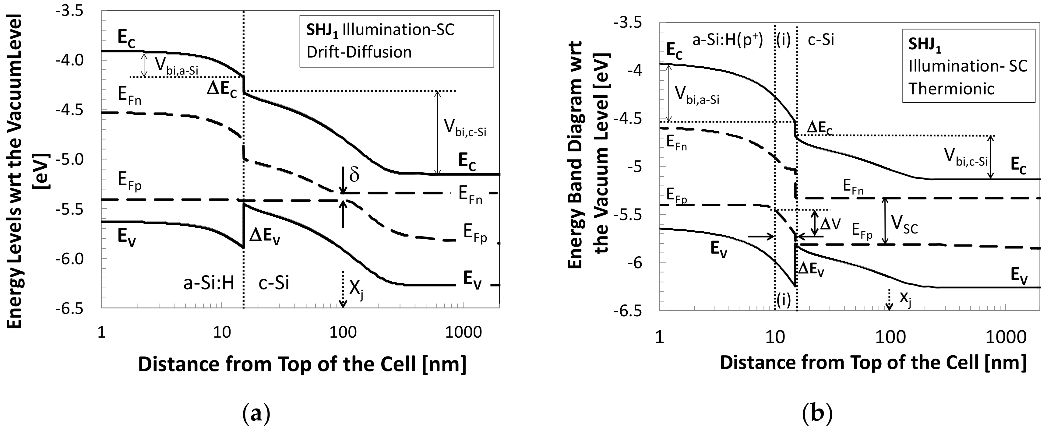
3.2.2. Energy Band Diagrams under Illumination

The energy band diagram simulated for cell SHJ1 and displayed in Figure 5a at non-equilibrium under AM1.5G illumination and short circuit conditions (illumination-SC), and assuming drift diffusion hole transport indicates the presence of a quasi-Fermi energy split δ, or equivalently a forward bias, amounting to 80 mV on the pn junction, despite the short circuit condition. Such a bias is established in order to compensate the voltage drop on the cell dark series resistance Rs and hence to satisfy the cell closed loop equation with short circuit terminals. Therefore, δ represents the minimum junction bias at short circuit condition irrespectively of the transport mechanism and of the a-Si:H doping level. The value of Rs is estimated from Ohm’s law
Rs =δ/ISC
to 1.9 Ω cm2, which accounts for the resistance of the bulk and of the back contact. Although such a resistance is relatively high and can be reduced to less than half this value if the back contact is optimized, it will be maintained throughout the present work. On the other hand, a much larger quasi-Fermi energy split, designated by VSC in the band diagram of Figure 5b, has been reported when thermionic emission hole transport is considered, and qualitatively linked to hole reflection at the hetero-interface [35]. A clear interpretation, however, is still needed for the exact process leading to the creation of Vsc and for its dependence on the a-Si:H(p+) doping concentration and on the applied bias. In addition, as can be deduced from Figure 5b and as listed in Table 2, the built-in potentials Vbi,c-Si in c-Si and Vbi,a-Si in a-Si:H at short circuit condition are quite different from their values at equilibrium depicted in Figure 2a and listed Table 1 when thermionic emission transport is assumed, while they remain practically unchanged under drift-diffusion transport, as shown in Figure 5a. Such changes in the built-in potentials may significantly affect the hole profiles, which is relevant to the investigation under study, and hence need to interpreted. Finally, it is useful to reiterate that such important differences between the band diagrams in Figure 5a resulting from simulations assuming drift-diffusion transport and in Figure 5b assuming thermionic emission transport result from the hetero-interface being considered as a boundary in the latter case, as explained in Section 3.2.

4. Enhanced Series Resistance Model

As mentioned earlier, hole reflection at the hetero-interface has been suggested to be the origin of the forward bias established at the pn junction under illumination and was taken as a basis for a model that interprets the FF degradation due to the thermionic emission barrier at the a-Si:H/c-Si hetero-interface [35]. So far, however, such a model lacks answers to the several questions raised in the introduction. An attempt is made in the following analysis to develop a higher level model that gives acceptable and justified answers to these questions.

4.1. Enhanced a-Si:H Resistance under Illumination and Its Relationship with Hole Reflection at the Thermionic Barrier

By inspecting the band diagrams of Figure 5a,b more closely, following the behavior of the hole quasi-Fermi energy and the quasi-Fermi energy split at the junction, and studying the cell short circuit closed loop equation, the forward bias VSC at the junction should be given by
VSC = Va-Si + δ
VSC = ΔV + Va-Si(p+) + δ
where Va-Si is the total voltage drop on the double a-Si:H layer, ΔV is the sharp voltage drop on the a-Si:H(i) layer, well identified in the band diagram of Figure 5b, and Va-Si(p+) is the voltage drop on the doped a-Si:H(p+) layer. As concluded in Section 3.2.1, the presence of a naturally high dark a-Si:H resistance that justifies the voltage drop Va-Si is ruled out, since it does not show when drift-diffusion transport is assumed. Consequently, the voltage drop on the double a-Si:H layer could only be explained by the presence of an enhanced a-Si:H resistance under illumination. The origin of such enhanced resistance and its exclusive occurrence under thermionic emission transport needs to be clarified.
The hole concentration profile in cell SHJ1 displayed in Figure 6a shows that, when thermionic emission transport is assumed, the peak hole concentration ppeak at the hetero-interface increases from typically 8.55 × 1018 cm−3 at equilibrium to 3.74 × 1019 cm−3 under illumination-SC, which represents a substantial boost of 400%. On the other hand, the value of ppeak practically does not change from its equilibrium value when drift-diffusion hole transport is assumed, and is maintained around 8.7 × 1018 cm−3. Therefore, such a boost in ppeak under thermionic emission transport can surely be attributed to incomplete hole collection, or equivalently to holes reflected at the thermionic barrier and piling-up as excess holes at the hetero-interface. These excess holes create a dipole with the negative acceptor ions in the doped a-Si:H(p+) that enhances the electric field crossing the a-Si:H(i) layer well above its value at equilibrium, as depicted in Figure 6b. Such a high field repels the free holes spilling-over in a-Si:H(i) back towards the a-Si:H(p+) layer, causing full depletion of the a-Si:H(i) layer, which explains the very low and flat hole concentration as well as the very high and flat field distribution in the layer depicted in Figure 6a,b, respectively. The enhanced electric field causes further depletion of the a-Si:H(p+) layer and decays gradually as it penetrates deeper in the layer. Consequently, the resistance of the double a-Si:H layer is strongly enhanced, which justifies the voltage drop Va-Si of Equation (4a), and may finally lead to a considerable increase in the cell series resistance that explains the distorted shape of the I-V characteristics displayed in Figure 4a. Furthermore, the integration of the enhanced and extended electric field in a-Si:H explains the increase in the built-in potential in a-Si:H, Vbi,a-Si, compared to its value at equilibrium, as discussed in Section 3.2.2. Such an increase is balanced by a decrease in the built-in potential in c-Si, Vbi,c-Si, in order to force the total built-in potential at short circuit to be equal to its value at equilibrium, taking into account the dark resistance voltage drop δ, as confirmed in Table 2.
At short circuit condition and using Equation (4a), the enhanced a-Si:H resistance R a S i is determined from
R a S i = V SC δ I S C
where VSC is to be extracted from the band diagram under illumination-SC, δ to be accurately determined from the band diagram under drift diffusion transport or evaluated knowing the dark series resistance, and ISC determined from the I-V characteristics under illumination. Typically, R a S i in cell SHJ1 is estimated to 9 Ω cm2. In addition, the latter is to be divided into (1) a dominant a-Si:H(i) resistance given by
R a S i ( i ) = Δ V I S C
and (2) a resistance of the depleted region in the a-Si:H(p+) layer to be determined from
R a S i ( p + ) = R a S i   R a S i ( i ) .
Hence, R a S i ( i ) can be estimated with ΔV in Equation (5b) extracted from the band diagram of Figure 5b, or can be calculated knowing the low flat free hole concentration in the a-Si:H(i) layer in Figure 6a and the layer thickness. Finally, R a S i ( p + )   follows from Equation (5c). Typically, R a S i ( i )   and R a S i ( p + ) in SHJ1 at short circuit are estimated to be 6.25 and 2.75 Ω cm2, respectively. It is worth noting that the hole profile, the electric field, and the built-in potential close to the interface remain intact when drift-diffusion transport is assumed, which confirm the proposed relationship between hole reflection at the thermionic barrier and the enhanced a-Si:H series resistance under illumination.
Finally, the proposed enhanced resistance model developed here explains clearly that the forward bias VSC revealed in [35] is compensated in the cell closed loop at short circuit or at any bias by the voltage drop on the enhanced a-Si:H resistance. In addition, it also becomes clear that, since the effect of hole reflection at the thermionic emission barrier is finally assimilated to the effect of an enhanced series resistance, the fact that only the cell FF is degraded while the cell open circuit voltage is not affected is now clarified.

4.2. Model Verification and Predictions

4.2.1. Impact of the Probability of Hole Reflection

The point here is just to confirm that the proposed model operates systematically and consistently. By inspecting Table 3 and the inserts in Figure 6a and in Figure 7a, it appears that under illumination and thermionic emission transport ppeak in SHJ1 decreases from 3.74 × 10¹⁹ to 1.86 × 1019 cm−3 when A* increases from 9.56 to 20 A K−2 cm−2 due to reduced reflection. The weaker dipole and reduced electric field enhancement confirmed in Figure 7b and in Table 3 lead to less depletion of the double a-Si:H layer, as depicted in Figure 7a compared to Figure 6a, and hence to a smaller enhancement in the resistance of the double a-Si:H layer, as listed in Table 3, which leads to an improvement in the I-V characteristics depicted in Figure 8. As expected, only at very large values of A*, i.e., when the reflection probability is very small, the cell series resistance is determined only by its value in the dark and the I-V characteristics tend to converge with those obtained assuming drift-diffusion transport.

4.2.2. Impact of the Thickness of the Intrinsic a-Si:H(i) Layer

The results of the simulations of cell SHJ1 show that reducing the thickness of the a-Si:H(i) layer (ti) while fixing the probability of hole reflection at the hetero-interface results in larger values of ppeak and of the electric field at equilibrium, as shown in Table 4. Under illumination-SC, however, the total value of ppeak including the reflected holes as well as the enhanced electric field at the hetero-interface are practically independent of ti,, as seen in Table 4. Therefore, the relative boost in the electric field decreases from 100% when ti = 5 nm to 61% when ti = 2 nm and to 37% when the a-Si:H(i) layer is totally omitted. The field enhancement, however, is still large enough to fully deplete the a-Si:H(i) layer and hence to enhance its resistance. As the layer thickness is reduced, however, its resistance decreases proportionally which forces VSC to decrease as confirmed in Table 4. The total a-Si:H enhanced resistance R a S i estimated using Equation (5a), its components R a S i ( i ) in a-Si:H(i) estimated using Equation (5b), and R a S i ( p + ) in a-Si:H(p+) estimated using Equation (5c) are listed, respectively, in Columns A, B, and C of Table 4. The value of R a S i ( p + )   is practically independent of ti and falls in the range 2.7 to 2.85 Ω cm2, which is expected since the a-Si:H(i) layer is fully depleted and hence its thickness does not influence the electric field passing through. When the a-Si:H(i) layer is totally omitted, the value of R a S i ( p + )   is estimated to be 2.55 Ω cm2, which is slightly smaller since all free holes in a-Si:H are confined now inside the doped layer. Note that the voltage drop δ attributed to dark cell series resistance at short circuit condition remains unaffected by the a-Si:H(i) thickness, which confirms that the dark resistance of the double a-Si:H layer is relatively small in the present case. The I-V characteristics simulated under illumination for different values of a-Si:H(i) thickness displayed in Figure 9 show a continuous increase in the FF from 40% when ti = 5 nm to 64% when the intrinsic layer is totally omitted. The latter value, however, is still small, which indicates that the excess hole depletion in the doped a-Si:H (p+) under illumination and the associated enhanced resistance still play an important role in the FF degradation even if the intrinsic a-Si:H(i) layer is removed.

4.2.3. Bias Dependence of the Cell Series Resistance

Under illumination, the total inversion layer peak hole concentration ppeak starts to decrease when the forward bias applied to the cell exceeds 0.2 V, as depicted in Figure 10a and listed in Table 5, which leads to a weaker excess dipole and reduced enhancement in the electric field at the hetero-interface, as depicted in Figure 10b and also shown in Table 5. Accordingly, the proposed model predicts less depletion of the double a-Si:H layer and smaller enhanced a-Si:H resistance with increasing the cell forward bias, which are both confirmed in Figure 10a and Table 5, respectively. The enhanced double a-Si:H layer resistance R a S i ( V ) is estimated as a function of the cell forward bias from
R a S i ( V ) = V j ( V ) I ( V ) × R S V I ( V )
where V is the cell terminal voltage, Vj(V) is the total bias at the junction to be extracted from the band diagram, and I(V) is the cell current to be extracted from the I-V characteristics. For instance, at short circuit condition V = 0, Vj(0) = VSC, I(0) = ISC, I(0) × Rs = δ such that Equation (6) reduces to Equation (5a). The resulting values of Ra-Si(V) listed in Table 5 for SHJ1 confirm that the enhanced a-Si:H resistance is bias-dependent, decreasing with increasing the forward bias, which explains the bias dependence of VSC.
The accuracy of the enhanced resistance model is checked by comparing the I-V characteristics of cell SHJ1 regularly simulated assuming thermionic emission transport, with the I-V characteristics of the same cell simulated assuming drift-diffusion transport with a bias dependent resistance, having the values listed in Table 5, connected in series with the cell. A perfect matching is obtained, as depicted in Figure 11, which confirms the validity of the approach and the accuracy of the model. The reference I-V characteristics of cell SHJ1 under drift-diffusion transport are also displayed in Figure 11 for comparison.

4.2.4. Dependence of the Enhanced a-Si:H Resistance on the Doping Concentration in a-Si:H(p+)

As discussed in Section 3.1 and depicted in Figure 3a,b, the equilibrium value of the peak inversion layer hole concentration ppeak at the hetero-interface and of the electric field are much larger in cell SHJ4 than in cell SHJ1. Since hole reflection is not expected to be very different in either cell at identical values of A*, of ΔEV, and of T, the relative increase in the hole concentration at the hetero-interface and the associated enhancement in the electric field upon hole reflection under illumination are expected to be much smaller in cell SHJ4 than in cell SHJ1. With such a smaller enhancement in the electric field, and with an initially much larger concentration of free holes spilling-over in a-Si:H(i), the depletion of the latter and of the a-Si:H(p+) layer is expected to be much less significant in SHJ4; consequently, the enhanced a-Si:H resistance is expected to be much smaller than in SHJ1. Moreover, at similar current, the voltage drop on R a S i would be much smaller in SHJ4, which will be reflected on the value of VSC. By interpolation, it can be concluded that the enhanced series resistance under illumination decreases continuously as the doping level in a-Si:H(p+) increases, which perfectly explains the doping dependence of VSC recorded and not interpreted in [35].
By inspecting the results of the simulations carried out for cell SHJ4 under illumination-SC, it appears that the value of ppeak is enhanced by 17% reaching 5.6 × 1019 cm−3 compared to 4.8 × 1019 cm−3 at equilibrium and that the electric field in a-Si:H(i) is enhanced by only 4% on the average, as depicted in Figure 12a,b, respectively. The value of VSC extracted from the simulated band diagram for cell SHJ4 under illumination-SC amounts to 104 mV including the 80 mV dark cell series resistance voltage drop δ, which results in a total enhanced a-Si:H resistance of 0.64 Ω cm2, mainly due to the partial depletion of the hole spill-over region in a-Si:H(i) layer, compared to 9 Ω cm2 in cell SHJ1. Finally, apart from the effect of δ, the expanded plot of the valence band diagram displayed in Figure 13 shows only a slight change in the built-in potential in a-Si:H and in c-Si under illumination-SC compared to the situation at equilibrium, which is consistent with the relatively small degradation of the FF in cell SHJ4 from 78.4% with drift-diffusion transport to 75.5% with thermionic emission transport. Such findings are consistent, agree perfectly with the model predictions and give a clear explanation to the doping dependence of the I-V characteristics depicted in Figure 4a.

5. Summary and Conclusions

A model is developed that accurately interprets the distortion of the I-V characteristics of SHJ cells under illumination linked to hole reflection at the thermionic emission barrier. In the proposed model, the reflected holes at the thermionic emission energy barrier pile up at the hetero-interface and create an excess dipole with negative ions in the a-Si:H(p+) layer. The enhanced electric field crossing the a-Si:H(i) layer sweeps the free holes spilling-over from the a-Si:H(p+) layer back, strongly depleting the intrinsic layer and widening the depletion of the doped layer, which enhance the total cell series resistance. With such a model, the large forward bias VSC established at the pn junction even at short circuit terminals compensates the voltage drop on the enhanced series resistance under illumination. Also, since the model explains the bias dependence of VSC, which follows that of the enhanced a-Si:H resistance linked to the bias dependence of the excess electric field at the hetero-interface. In addition, the model predicts that cells with heavily doped a-Si:H(p+) would suffer less from hole reflection at the thermionic emission under illumination because the relative excess hole concentration piling-up at the hetero-interface is smaller. Therefore, the enhanced field, a-Si:H depletion and resistance are undermined, which results in smaller values of VSC and to improved I-V characteristics and cell FF.
Moreover, since the proposed model assimilates the impact of hole reflection at the thermionic barrier to a series resistance effect, it gives an answer to why only the cell FF is degraded, while the cell open circuit is unaffected. Accordingly, the degradation associated with the thermionic barrier can be clearly differentiated from that related to the front Schottky contact in the presence of an inadequate TCO usually characterized by a degradation in both the Voc and the FF.

Author Contributions

Both authors have made significant contribution to this study and have approved this submission. M.G. originated the idea and defined the methodology. Both authors contributed to running the simulations and in discussing and validating the interpretations. Conceptualization: M.G.; data curation: M.G.; formal analysis: M.G.; funding acquisition: Y.A.; investigation: M.G. and Y.A.; methodology: M.G.; project administration: Y.A.; software: M.G. and Y.A.; validation: M.G. and Y.A.; writing—original draft: M.G.; writing—review & editing: M.G.

Funding

This research was funded by Kuwait Foundation for the Advances of Science [KFAS] grant number [P115-15EE-01].

Acknowledgments

This work is supported by the Kuwait University Research Administration project GE01/08 and the KFAS/KU-IMEC funded project P115-15EE-01.

Conflicts of Interest

The authors declare no conflict of interest.

References

  1. Ghannam, M.; Nijs, J.; Mertens, R.; DeKeersmaecker, R. A silicon bipolar transistor with a hydrogenated amorphous emitter. In Proceedings of the International Electron Device Meeting, San-Francisco, CA, USA, 3–7 December 1984; IEEE: Piscataway, NJ, USA, 1984; pp. 746–748. [Google Scholar]
  2. Ghannam, M.; Mertens, R.; Nijs, J. Method of producing a bipolar transistor having an amorphous emitter formed by plasma CVD. U.S. Patent 5,108,936, 28 April 1992. [Google Scholar]
  3. Wakisaka, K.; Taguchi, M.; Sawada, T.; Tanaka, M.; Matsuyama, T.; Matsuoka, T.; Tsuda, S.; Nakano, S.; Kishi, Y.; Kuwano, Y. More than 16% solar cells with a new “HIT” (doped a-Si/nondoped a-Si/crystalline Si) structure. In Proceedings of the 22nd IEEE Photovoltaic Specialists Conference, Las Vegas, NV, USA, 7–10 October 1991; IEEE: Piscataway, NJ, USA, 1991; pp. 887–892. [Google Scholar]
  4. Tanaka, M.; Taguchi, M.; Matsuyama, T.; Sawada, T.; Tsuda, S.; Nakano, S.; Hanafusa, H.; Kuwano, Y. Development of new a-Si/c-Si heterojunction solar cells: ACJ-HIT (Artificially constructed junction-heterojunction with intrinsic thin-layer. Jpn. J. Appl. Phys. 1992, 31, 3518–3522. [Google Scholar] [CrossRef]
  5. Taguchi, M.; Yano, A.; Tohoda, S.; Matsuyama, K.; Nakamura, Y.; Nishiwaki, T.; Fujita, K.; Maruyama, E. 24.7% Record Efficiency HIT Solar Cell on Thin Silicon Wafer. IEEE J. Photovolt. 2014, 4, 96–99. [Google Scholar] [CrossRef]
  6. Masuko, K.; Shigematsu, M.M.; Hashiguchi, T.; Fujishima, D.; Kai, M.; Yoshimura, N.; Yamaguchi, T.; Ichihashi, Y.; Mishima, T.; Matsubara, N.; et al. Achievement of more than 25% conversion efficiency with crystalline silicon heterojunction solar cell. IEEE J. Photovolt. 2014, 4, 1433–1435. [Google Scholar] [CrossRef]
  7. Yoshikawa, K.; Yoshida, W.; Irie, T.; Kawasaki, H.; Konishi, K.; Ishibashi, H.; Asatani, T.; Adachi, D.; Kanematsu, M.; Uzu, H.; et al. Exceeding efficiency of 26% by heterojunction interdigitated back contact solar cell with thin film Si technology. Sol. Energy Mater. Sol. Cells 2017, 173, 37–42. [Google Scholar] [CrossRef]
  8. Ghannam, M.; Shehada, G.; Abdulraheem, Y.; Poortmans, J. On the possible role of the interfacial inversion layer in the improvement of the performance of hydrogenated amorphous silicon/crystalline silicon heterojunction solar cells [HIT]. Sol. Energy Mater. Sol. Cells 2015, 132, 320–328. [Google Scholar] [CrossRef]
  9. Ghosh, K.; Tracy, C.; Herasimenka, S.; Honsberg, C.; Bowden, S. Explanation of the device operation principle of amorphous silicon/crystalline silicon heterojunction solar cell and role of the inversion of crystalline silicon surface. In Proceedings of the 35th IEEE Photovoltaic Specialists Conference, Honolulu, HI, USA, 20–25 June 2010; IEEE: Piscataway, NJ, USA, 2010; pp. 1383–1386. [Google Scholar]
  10. Hareland, S.A.; Jallepalli, S.; Chindalore, G.; Shih, W.K.; Tasch, A.F.; Maziar, C.M., Jr. A Simple Model for Quantum Mechanical Effects in Hole Inversion Layers in Silicon PMOS Devices. IEEE Trans. Electron. Dev. 1997, 44, 1172–1173. [Google Scholar] [CrossRef]
  11. Van Dort, M.J.; Woerlee, P.H.; Walker, A.J. A simple model for quantization effects in heavily-doped silicon MOSFET’s at inversion conditions. Solid-State Electron. 1994, 37, 411–414. [Google Scholar] [CrossRef]
  12. Ghannam, M.; Abdulraheem, Y.; Shehada, G. Interpretation of the degradation of silicon HIT solar cells due to inadequate front contact TCO work function. Sol. Energy Mater. Sol. Cells 2016, 145, 423–431. [Google Scholar] [CrossRef]
  13. Rossler, R.; Leendetz, C.; Korte, L.; Mingirulli, N.; Rech, B. Impact of the transparent conductive oxide work function on injection-dependent a-Si:H/c-Si band bending and solar cell parameters. J. Appl. Phys. 2013, 113, 144513. [Google Scholar] [CrossRef]
  14. Varache, R.; Kleider, J.P.; Gueunier-Farret, M.E.; Korte, L. Silicon heterojunction solar cells: Optimization of emitter and contact properties from analytical calculation and numerical simulation. Mater. Sci. Eng. 2013, B178, 593–598. [Google Scholar] [CrossRef]
  15. Delahoy, A.E.; Stavrides, A.P.; Patel, A.M.; Le, L.T.; Cambridge, J.A.; Xu, Y.; Guo, S. Influence of TCO type on the performance of amorphous silicon solar cells. In Proceedings of the SPIE 7045, Photovoltaic Cell and Module Technologies II, San Diego, CA, USA, 10 September 2008; p. 704506. [Google Scholar]
  16. Zhao, L.; Zhou, C.L.; Li, H.L.; Diao, H.W.; Wang, W.J. Role of the work function of transparent conductive oxide on the performance of amorphous/crystalline silicon heterojunction solar cells studied computer simulation. Phys. Status Solidi (A) 2008, 205, 1215–1221. [Google Scholar] [CrossRef]
  17. Klein, A.; Korber, C.; Wachau, A.; Sauberlich, F.; Gassenbauer, Y.; Harvey, S.; Proffit, D.; Mason, T. Transparent conducting oxides for photovoltaics: Manipulation of fermi level, work function and energy band alignment. Materials 2010, 3, 4892–4914. [Google Scholar] [CrossRef] [PubMed]
  18. Smole, F.; Topic, M.; Furlan, J. Analysis of TCO/p(a-SiC:H) heterojunction and its influence on p-i-n a-Si:H solar cell performance. J. Non-Cryst. Solids 1996, 194, 312–318. [Google Scholar] [CrossRef]
  19. Corpus-Mendoza, A.N.; DeSouza, M.M.; Hamelmann, F.U. Design of Schottky contacts for optimum performance of thin-film silicon solar cells. IEEE J. Photovolt. 2015, 5, 22–27. [Google Scholar] [CrossRef]
  20. Minami, T.; Miyata, T.; Yamamoto, T. Work function of transparent conducting multi component oxide thin films prepared by magnetron sputtering. Surf. Coat. Technol. 1998, 108–109, 583–587. [Google Scholar]
  21. Barraud, L.; Holman, Z.C.; Badel, N.; Descoeudres, A.; Battaglia, C.; De Wolf, S.; Ballif, C. Hydrogen-doped indium oxide/indium tin oxide bilayers for high-efficiency silicon heterojunction solar cells. Sol. Energy Mater. Sol. Cells 2013, 115, 151–156. [Google Scholar] [CrossRef] [Green Version]
  22. Ganguly, G.; Carlson, D.E.; Hegedus, S.S.; Ryan, D.; Gordon, R.G.; Pang, D.; Reedy, R.C. Improved fill factors in amorphous silicon solar cells on zinc oxide by insertion of a germanium layer to block impurity incorporation. Appl. Phys. Lett. 2004, 85, 479–481. [Google Scholar] [CrossRef]
  23. Im, J.-S.; Jeon, J.-W.; Park, S.; Lee, Y.; Lim, K.S. Improvement of amorphous silicon solar cell performance by inserting a tungsten oxide layer between zinc oxide and p-type amorphous silicon carbide. In Proceedings of the 37th IEEE Photovoltaic Specialists Conference, Seattle, WA, USA, 19–24 June 2011; IEEE: Piscataway, NJ, USA; pp. 612–615. [Google Scholar]
  24. Mimura, H.; Hatanaka, Y. Carrier transport mechanisms of p-type amorphous–n-type crystalline silicon heterojunctions. J. Appl. Phys. 1992, 71, 2315–2320. [Google Scholar] [CrossRef]
  25. Van Cleef, M.W.M.; Schropp, R.E.I.; Rubinelli, F.A. Significance of tunneling in p+ amorphous silicon carbide n crystalline silicon heterojunction solar cells. Appl. Phys. Lett. 1998, 73, 2609–2611. [Google Scholar] [CrossRef]
  26. Kanevce, A.; Metzger, W.K. The role of amorphous silicon and tunneling in heterojunction with intrinsic thin layer (HIT) solar cells. J. Appl. Phys. 2009, 105, 094507. [Google Scholar] [CrossRef]
  27. Matsuura, H.; Okuno, T.; Okushi, H.; Tanaka, K. Electrical properties of n-amorphous/ p-crystalline silicon heterojunctions. J. Appl. Phys. 1984, 55, 1012–1019. [Google Scholar] [CrossRef]
  28. Schulze, F.; Korte, L.; Conrad, E.; Schmidt, M.; Rech, B. Electrical transport mechanisms in a-Si:H/c-Si heterojunction solar cells. J. Appl. Phys. 2010, 107, 023711. [Google Scholar] [CrossRef]
  29. Rubinelli, F.; Albornoz, S.; Buitrago, R. Amorphous-crystalline silicon heterojunction: Theoretical evaluation of the current terms. Solid-State Electron. 1989, 32, 813–825. [Google Scholar] [CrossRef]
  30. Taguchi, M.; Maruyama, E.; Tanaka, M. Temperature Dependence of Amorphous/Crystalline Silicon Heterojunction Solar Cells. Jpn. J. Appl. Phys. 2008, 47, 814–819. [Google Scholar] [CrossRef]
  31. Mews, M.; Liebhaber, M.; Rech, B.; Korte, L. Valence band alignment and hole transport in amorphous/crystalline silicon heterojunction solar cells. Appl. Phys. Lett. 2015, 107, 013902. [Google Scholar] [CrossRef] [Green Version]
  32. Rahmouni, M.; Datta, A.; Chatterjee, P.; Damon-Lacoste, J.; Ballif, C.; Roca i Cabarrocas, P. Carrier transport and sensitivity issues in heterjunction with intrinsic thin layer solar cells on N-type crystalline silicon. A computer simulation study. J. Appl. Phys. 2010, 107, 054521. [Google Scholar] [CrossRef]
  33. Stangl, R.; Froitzheim, A.; Kriegel, M.; Brammer, T.; Kirste, S.; Elstner, L.; Stiebig, H.; Schmidt, M.; Fuhs, W. AFORS-HET, a numerical PC-program for simulation of heterojunction solar cells. In Proceedings of the 19th European Photovoltaic Solar Energy Conference, Paris, France, 7–11 June 2004; pp. 1497–1500. [Google Scholar]
  34. Stangl, R.; Leendertz, C.; Haschke, J. Numerical simulation of solar cells and solar cell characterization; The open-source on demand program AFORS-HET. In Solar Energy; Rugescu, R.D., Ed.; Intech: Vukovar, Croatia, 2012; pp. 319–352. [Google Scholar]
  35. Ghannam, M.; Abdulraheem, Y. Fundamental constraints imposed by energy barriers on the fill factor and on the efficiency of silicon heterojunction solar cells. Sol. Energy Mater. Sol. Cells 2017, 171, 228–238. [Google Scholar] [CrossRef]
  36. Tucci, M.; Serenelli, L.; De Iuliis, S.; Izzi, M.; De Cesare, G.; Caputo, D. Contact formation on a-Si:H/c-Si heterostructure solar cells. In Physics and Technology of Amorphous-Crystalline Heterostructure Silicon Solar Cells; Sark, W.J.H.M., Korte, L., Roca, F., Eds.; Springer: Berlin/Heidelberg, Germany, 2012; pp. 331–375. ISBN 978-3-642-22274-0. [Google Scholar]
  37. Korte, L. Electronic properties of ultrathin a-Si:H layers and the a-Si:H/c-Si interface. In Physics and Technology of Amorphous-Crystalline Heterostructure Silicon Solar Cells; Sark, W.J.H.M., Korte, L., Roca, F., Eds.; Springer: Berlin/Heidelberg, Germany, 2012; pp. 161–221. ISBN 978-3-642-22274-0. [Google Scholar]
  38. Sebastiani, M.; Di Gaspare, L.; Capellini, G.; Bittencourt, C.; Evangelisti, F. Low-Energy Yield Spectroscopy as a Novel Technique for Determining Band Offsets: Application to the c−Si(100)/a−Si:H Heterostructure. Phys. Rev. Lett. 1995, 75, 3352–3355. [Google Scholar] [CrossRef] [PubMed]
  39. Bittencourt, C.; Alvarez, F. Properties of Amorphous Silicon and Its Alloys; Searle, T., Ed.; The IEE Emis Datareviews: London, UK, 1998; ISBN 0852969228. [Google Scholar]
  40. Stutzmann, M.; Biegelsen, D.; Street, R. Detailed investigation of doping in hydrogenated amorphous silicon and germanium. Phys. Rev. B 1987, 35, 5666–5701. [Google Scholar] [CrossRef]
  41. Caputo, D.; De Cesare, G.; Irrera, F.; Nascetti, A.; Palma, F. On the relation between defect density and dopant concentration in amorphous silicon films. J. Non-Cryst. Solids 2000, 266–269, 565–568. [Google Scholar] [CrossRef]
  42. Milnes, A.G.; Feucht, D.L. Heterojunction and Metal-Semiconductor Junctions; ScienceDirect: New York, NY, USA, 1972; ISBN 9780124980501. [Google Scholar]
  43. Kleider, J.P. Band lineup theories and the determination of band offsets from electrical measurements. In Physics and Technology of Amorphous-Crystalline Heterostructure Silicon Solar Cells; Sark, W.J.H.M., Korte, L., Roca, F., Eds.; Springer: Berlin/Heidelberg, Germany, 2012; pp. 405–444. ISBN 978-3-642-22274-0. [Google Scholar]
  44. Maslova, O.A.; Alvarez, J.; Gushina, E.V.; Favre, W.; Gueunier-Farret, M.E.; Gudovskikh, A.S.; Ankudinov, A.V.; Terukov, E.I.; Kleider, J.P. Observation by conductive-probe atomic force microscopy of strongly inverted surface layers at the hydrogenated amorphous silicon/crystalline silicon heterojunctions. Appl. Phys. Lett. 2010, 97, 252110. [Google Scholar]
  45. Li, J.; Crandall, R.; Young, D.; Page, M.; Iwaniczko, E.; Wang, Q. Capacitance study of inversion at the amorphous-crystalline interface of n-type silicon heterojunction solar cells. J. Appl. Phys. 2011, 110, 114502. [Google Scholar] [CrossRef] [Green Version]
  46. Maslova, O.; Brézard-Oudot, A.; Gueunier-Farret, M.E.; Alvarez, J.; Favre, W.; Muñoz, D.; Kleider, J.P. Understanding inversion layers and band discontinuities in hydrogenated amorphous silicon/crystalline silicon heterojunctions from the temperature dependence of the capacitance. Appl. Phys. Lett. 2013, 103, 183907. [Google Scholar] [CrossRef]
  47. Oldham, W.G.; Milnes, A.G. N-n semiconductor heterojunctions. Solid-State Electron. 1963, 6, 121–132. [Google Scholar] [CrossRef]
  48. Van Opdorp, C.; Kanerva, H.K.J. Current-voltage characteristics and capacitance of isotype heterojunctions. Solid-State Electron. 1967, 10, 401–421. [Google Scholar] [CrossRef]
  49. Gil, M.; Yang, J.; Kleiman, R.N. Analytical expression for thermionic transport through isotype heterojunction interfaces of arbitrary doping ratio. IEEE Trans. Electron. Dev. 2014, 61, 198–201. [Google Scholar] [CrossRef]
  50. Schuelke, R.J.; Lundstrom, M.S. Thermionic emission-diffusion theory of isotype heterojunctions. Solid-State Electron. 1984, 27, 1111–1116. [Google Scholar] [CrossRef]
  51. Horio, K.; Yanai, H. Numerical modeling of heterojunctions including the thermionic emission mechanism at the hetero-junction interface. IEEE Trans. Electron. Dev. 1990, 37, 1093–1098. [Google Scholar] [CrossRef]
  52. Chang, K.-M.; Tsai, J.-Y.; Chang, C-.Y. New physical formulation of the thermionic emission current at the heterojunction interface. IEEE Electron Dev. Lett. 1993, 14, 338–341. [Google Scholar] [CrossRef]
  53. Berz, F. The Bethe condition for thermionic emission near an absorbing boundary. Solid-State Electron. 1985, 28, 1007–1013. [Google Scholar] [CrossRef]
  54. Yang, K.; East, J.R.; Haddad, G.I. Numerical modeling of abrupt heterojunctions using a thermionic-field emission boundary condition. Solid-State Electron. 1993, 36, 321–330. [Google Scholar] [CrossRef]
  55. Schottky, W. Semicondutor theory of the barrier layer. Nat. Sci. 1938, 26, 843. [Google Scholar] [CrossRef]
  56. Guo, S.F. A simple model for computer simulation of Schottky-barrier diodes. Solid State Electron. 1984, 27, 537–543. [Google Scholar] [CrossRef]
  57. Simmons, J.G.; Taylor, G.W. Generalized theory of conduction in Schottky barriers. Solid State Electron. 1983, 26, 705–709. [Google Scholar] [CrossRef]
  58. Bethe, H.A. MIT Radiation Lab. Report 1942, 43, 12. [Google Scholar]
  59. Crowell, C.R.; Sze, S.M. Current transport in metal-semiconductor barriers. Solid-State Electron. 1966, 9, 1035–1048. [Google Scholar] [CrossRef]
  60. Crowell, C.R.; Beguwala, M. Recombination velocity effects on current diffusion and imref in Schottky barriers. Solid State Electron. 1971, 14, 1149–1157. [Google Scholar] [CrossRef]
  61. Crowell, C.R.; Sze, S.M. Quantum-mechanical reflection of electrons at metal-semiconductor barriers: Electron transport in semiconductor-metal-semiconductor structures. J. Appl. Phys. 1966, 37, 2683–2689. [Google Scholar] [CrossRef]
  62. Grinberg, A.A.; Luryi, S. On electron transport across connecting materials with different effective masses. IEEE Trans. Electron. Dev. 1998, 45, 1561–1568. [Google Scholar] [CrossRef]
  63. Shannon, J.M.; Nieuwesteeg, K.J.B.M. Tunneling effective mass in hydrogenated amorphous silicon. Appl. Phys. Lett. 1993, 62, 1815–1817. [Google Scholar] [CrossRef]
  64. Maeda, K.; Chiyoda, W.; Umezu, I.; Kuroe, A. Depletion layer width in a-Si:H Schottky barrier revealed by reverse bias photocurrent. J. Appl. Phys. 1994, 75, 3522–3529. [Google Scholar] [CrossRef]
  65. Aflatooni, K.; Hornsey, R.; Nathan, A. Reverse Current Instabilities in Amorphous Silicon Schottky Diodes: Modeling and Experiments. IEEE Trans. Electron Dev. 1999, 46, 1417–1422. [Google Scholar] [CrossRef]
Figure 1. Silicon hetero-junction (SHJ) solar cell under study (simulations done with TCO removed).
Applsci 08 01846 g001
Figure 2. Simulated band diagrams at equilibrium for (a) cell SHJ1 [35] and (b) cell SHJ4.
Applsci 08 01846 g002
Figure 3. (a) Hole concentration profile, and (b) electric field distribution, simulated for cells SHJ1 and SHJ4 at equilibrium.
Applsci 08 01846 g003
Figure 4. (a) Simulated I-V characteristics under illumination at 300 K assuming thermionic emission transport for cells SHJ1 (Na-Si = 5 × 1018 cm−3), SHJ2 (Na-Si = 1019 cm−3), SHJ3 (Na-Si = 5 × 1019 cm−3), and SHJ4 (Na-Si = 1 × 1020 cm−3) [35]. (b) Simulated I-V characteristics under illumination at 300K for cell SHJ1 with Na-Si = 5 × 1018 cm−3: Thermionic emission transport (Curves 1, 2, and 3), drift-diffusion transport (Curve 4). Front contact: WFTCO = 5 eV (Curve 1) and 5.2 eV (Curve 2), flat band (Curves 3 and 4).
Applsci 08 01846 g004
Figure 5. Band diagrams obtained from AFORS-HET simulations of cell SHJ1 under illumination-SC with (a) drift-diffusion and (b) thermionic emission transport [35].
Applsci 08 01846 g005
Figure 6. Simulated (a) hole concentration profile and (b) electric field distribution, in cell SHJ1 under illumination-SC with thermionic emission transport (Dash) and drift-diffusion transport (also ~ equilibrium) (Cont. line).
Applsci 08 01846 g006
Figure 7. Results of AFORS-HET simulations of cell SHJ1 under illumination-SC: (a) hole concentration profile assuming thermionic emission with A* = 20 A K−2 cm−2 (Dash) and with drift-diffusion (Cont.); (b) electric field distribution with A* = 9.56 (default), 20 and 50 A/K−2 cm−2 and at equilibrium (Cont.).
Applsci 08 01846 g007
Figure 8. Simulated I-V characteristics under illumination for cell SHJ1 with thermionic emission transport for different values of the Richardson constant A*. The I-V characteristics assuming drift-diffusion (Curve 5) is also plotted for comparison.
Applsci 08 01846 g008
Figure 9. Simulated I-V characteristics under illumination for cell SHJ1 with thermionic emission hole transport for different values of a-Si:H(i) layer thickness.
Applsci 08 01846 g009
Figure 10. Simulated (a) hole concentration profile and (b) electric field distribution for cell SHJ1 under illumination for different cell forward bias.
Applsci 08 01846 g010
Figure 11. Simulated I-V characteristics under illumination for cell SHJ1 with 1. thermionic emission transport, 2. drift-diffusion transport, and 3. (Symb) drift-diffusion transport with Ra-Si(V) of Table 5 connected in series.
Applsci 08 01846 g011
Figure 12. Simulated (a) free hole concentration profile and (b) electric Field distribution at equilibrium (Cont. line) and under illumination-SC (Dash) for cell SHJ4 assuming thermionic emission hole transport at the hetero-interface with a default value of A*.
Applsci 08 01846 g012
Figure 13. Simulated valence band diagram of cell SHJ4 at equilibrium and under illumination-SC assuming thermionic emission transport across the hetero-interface with the default A* value.
Applsci 08 01846 g013
Table 1. Built-in potential and its components in cells SHJ1 and SHJ4 at equilibrium.
Cell: Na-Si [cm−3]AB(B−A)
WF_c-Si [eV]WF_a-Si [eV]Vbi,total [V]
SHJ1: 5 × 10184.2455.4141.169
SHJ4: 1 × 10204.2455.5801.335
CD(C+D)
Vbi,a-SI [V]Vbi,c-SI [V]Vbi,total [V]
SHJ1: 5 × 10180.2700.8991.169
SHJ4: 1 × 10200.3910.9441.335
Table 2. Built-in potential in cells SHJ1 and SHJ4 under illumination-SC.
Cell Na-Si [cm−3]Vbi,a-Si [V]Vbi,c-Si [V]Vbi,total = Vbi,a-Si + Vbi,c-Si + δ [V]
SHJ1: 5 × 10180.6090.4801.089 + 0.08 = 1.169
SHJ4: 1 × 10200.4130.8421.255 + 0.08 = 1.335
Table 3. Dependence of enhanced a-Si:H series resistance in SHJ1 on hole thermionic emission probability (A*).
VSC – δ
(δ = 80)
[mV]
ppeak [cm−3]Max.
E-Field
[kV/cm]
Rs
[Ω cm2]
FF [%]
I. EquilibriumN/A8.55 × 1018268N/AN/A
II. Illumination-SC
a) Drift-Diffusion


0


8.70 × 10¹⁸


271


1.9 (Dark Rs)


78
b) Thermionic
A* [A K−2 cm−2]
Ra-Si
9.563823.74 × 10195499.0040.00
201731.86 × 10193964.0860.35
50451.07 × 10193041.0673.70
70349.97 × 10182940.8075.30
120109.30 × 10182750.2576.52
Table 4. Enhanced cell resistance in cell SHJ1versus a-Si:H(i) thickness.
a-Si:H thick.
[nm]
VSC–δ
[mV]
ppeak
Equilibr.
[cm−3]
Max. E-Field
Equilibr.
[KV/cm]
ppeak
Illumin-SC
[cm−3]
Max. E-Field
Illumin-SC
[KV/cm]
ISC
[mA.cm−2]
A
Ra-Si
[Ω cm2]
B
Ra-Si(i)
[Ω cm2]
C = A-B
Ra-Si(p+)
[Ω cm2]
53828.55 × 10182683.74 × 101954942.349.006.252.75
43321.01 × 10192903.76 × 101955142.347.845.002.84
32781.19 × 10193143.77 × 101955242.346.563.752.81
22211.43 × 10193423.69 × 101955442.345.212.502.71
01082.09 × 10194073.99 × 101956043.852.55N/A2.55
Table 5. Dependence of Ra-Si in cell SHJ1 on forward bias.
V
[mV]
ppeak
[cm−3]
E-Field
[KV/cm]
Vj(V)
[mV]
I(V)
[mA/cm2]
δ(V) = I*1.9
[mV]
Va-Si =
Vj(V)-δ-V
[mV]
Ra-Si (V) = Va-Si/I
[Ω cm2]
03.74 × 101954946242.380.03829.03
1003.74 × 101954956242.380.03829.03
2003.70 × 101954165141.378.53739.03
3003.65 × 101950869936.970.13298.90
4003.22 × 101945771930.758.32618.50
5002.61 × 101940072924.446.41837.50
6002.00 × 101933973518.334.81005.56
7001.44 × 10192807409.017.1232.55

