Further Investigations into the Capacitive Imaging Technique Using a Multi-Electrode Sensor


Center for Offshore Engineering and Safety Technology, China University of Petroleum, Qingdao 266580, China
*
Author to whom correspondence should be addressed.
Appl. Sci. 2018, 8(11), 2296; https://doi.org/10.3390/app8112296
Submission received: 30 September 2018
/
Revised: 2 November 2018
/
Accepted: 15 November 2018
/
Published: 19 November 2018
(This article belongs to the Special Issue Nondestructive Testing and Imaging Based on Electromagnetic Fields and Waves)
Abstract
:As a novel non-destructive testing technique, capacitive imaging (CI) has been used to detect defects within the insulation layer and metal surface of an insulated metallic structure, that is, pipe or vessel. Due to the non-linearity of the probing field, the defects at different depths in the insulation layer are difficult to compare accurately using the conventional CI sensor with a single pair of electrodes. In addition, the conventional CI sensor cannot provide adequate information to discriminate the defects in the insulation layer and metal surface. In order to solve the above-mentioned problems, the multi-electrode sensor is introduced. The multi-electrode sensor uses multiple quasi-static fringing electric fields generated by an array of coplanar electrodes to obtain extra information about the defects in the specimen. In this work, the feasibility of multiple quasi-static electric fields detecting the defects was demonstrated and the Measurement Sensitivity Distributions (MSDs) of the multi-electrode sensor detecting the defects were acquired using the FEM models. The simulation and experimental results show that the Dynamic Change Rates (DCRs) of the measured values obtained at the center of the defects in the insulator layer and metal surface present different variation patterns, which can be used to discriminate these two different kinds of defects. The reasons for the different variation patterns of DCRs were explained by the changing trends of MSDs with increased electrode separation. In addition, it was demonstrated that the different depths of the defects in the insulator layer can be compared accurately by comprehensive analysis of the detection results from all the electrode pairs.
1. Introduction
Insulation layer is a protective structure for metal pipeline to resist corrosion [1,2,3]. It is used to insulate metal pipeline from corrosion environment such as moisture content, to restrain the occurrence of corrosion on the surface of metal pipeline and finally to achieve the purpose of controlling corrosion [4]. Due to defects in pipeline production, external mechanical action, disturbance or pressure of soil, wear of rock, bacterial invasion and other factors, the defects of the insulator layer and metal surface often occur [5,6,7,8]. Therefore, it is very useful to detect the defects both in insulator layer and metal surface. When there are defects in the insulator layer, it is necessary to replace the insulator layer. When there are defects in the metal surface, it is necessary to replace the insulator layer and metal pipeline at the same time. Discriminating the defects in the insulator layer and metal surface is thus beneficial to take appropriate remedial measures to reduce maintenance cost and improve production efficiency [9]. It is a challenging work for conventional NDE technique and capacitive imaging (CI) technique has been proven to be a feasible technique in previous work [10,11,12,13].
As a novel non-destructive testing (NDT) technique, CI has been used for oil pipelines, storage tanks, nuclear power stations and new armor in recent years [14,15,16,17,18]. It has many advantages, such as easy to implement, cost effective, environment friendly and non-contact [10,12]. The CI can not only detect surface defects in a conductor but also detect internal defects in a non-conductor [11]. A conventional CI sensor consists of two co-planar electrodes, one being the driving electrode and the other being the sensing electrode [13]. The detection principle of CI is shown in Figure 1. An AC voltage is applied to the driving electrode and the sensing electrode is connected to a measurement circuit. As shown in Figure 1a, when the CI sensor detects a non-conducting specimen, the fringing electric field emanates from the driving electrode and terminates at the sensing electrode. The fringing electric field can reach the inside of the non-conducting specimen through the air gap. If there is a defect inside the non-conducting specimen, it will influence the distribution of the fringing electric field and thus impacts the charge on the sensing electrode. As shown in Figure 1b, when the CI sensor detects the conducting specimen covered by an insulation layer, the fringing electric field emanates from the driving electrode and terminates at the sensing electrode and on the surface of the conducting specimen. If a defect exists on the surface of the conducting specimen, it will also influence the distribution of the fringing electric field and thus impacts the charge on the sensing electrode. In summary, all the changes of the charge can be used to detect the defects within the insulation layer and metal surface. Note that for a clearer illustration, only the effective electric field lines, which originated from the driving electrode and terminated on the sensing electrode, were included in Figure 1. Field lines that terminated at the ground and infinity have minimal impact on the measured values and were omitted from the illustrative figure.
It is very difficult to accurately compare the defects at the different depths in the insulation layer and discriminate the defects within the insulation layer and metal surface using the conventional CI sensor with a single sensing electrode, because using a single pair of electrodes is hard to obtain more information about the defects. In order to solve the above problems, the multi-electrode sensor which can give more information about the defects in the depth direction was proposed and briefly introduced in Section 2. The finite element method (FEM) models were then constructed by COMSOL Multiphysics (COMSOL Co., Ltd.). The electric potential lines, measurement sensitivity distributions (MSDs), capacitances and dynamic change rate (DCRs) of the multi-electric sensor which was used to defect the defects were studied using FEM models in Section 3. CI experiments with the multi-electrode sensor were also carried out on a fiberglass composite specimen and an aluminum specimen covered by a fiberglass board. The experimental results are presented and discussed in Section 4. Discussions and conclusions are then presented in Section 5.
2. Principle of the Multi-Electrode Sensor for Defect Detection
The multi-electrode sensor uses multiple quasi-static fringing electric fields generated by an array of coplanar electrodes to acquire more information about the defects in the specimen and it has two different detection mechanisms according to the electrical conductivity of the specimens. Taking a four electrode sensor as an example, the detecting principle of the multi-electrode sensor is shown in Figure 2. An AC voltage is applied to the driving electrode and an array of the sensing electrodes are connected to a measurement circuit via a Multiplexer (MUX).
As shown in Figure 2a, when the specimen is non-conducting, the fringing electric field emanates from the driving electrode (No. 1) and terminates at the different sensing electrodes (No. 2–4). The three fringing electric fields between the driving electrode (No.1) and the different sensing electrodes (No. 2–4) are stratified, which can be used to acquire more information about the defects in the different electric fields. If a defect exists in a non-conducting specimen as shown in Figure 2a, the detecting results with the three sensing electrodes (No. 2–4) are different. The electric field between the driving electrode (No. 1) and the sensing electrode (No. 2) cannot detect the defect. The electric field between the driving electrode (No. 1) and the sensing electrode (No. 3) can detect the defect and the detecting result will show a trough in the process of a line scanning. The electric field between the driving electrode (No. 1) and the sensing electrode (No. 4) can also detect the defect but the detecting result will show two troughs in the process of a line scanning. Compared with these three line scans, it can be inferred that the defect is beyond the sensing limit of the driving electrode (No. 1) and the sensing electrode (No. 2) and within the sensing area of the driving electrode (No. 1) and the sensing electrode (No. 3). Thus its depth information will be approximated and that can be used to discriminate the different depths of the defects in non-conducting specimen.
As shown in Figure 2b, when the conducting specimen is covered by an insulation layer, the fringing electric field emanates from the driving electrode (No. 1) and terminates at the different sensing electrodes (No. 2–4) and on the surface of the conducting specimen. If a defect exists on the surface of the conducting specimen, it will influence the distribution of the different fringing electric fields and thus impacts the charge on the whole sensing electrodes (No. 2–4). The change on the charge of the different sensing electrodes contains more information about the defects, which may be used to discriminate the defects of the insulation layer and metal surface.
3. Simulation Analysis of the Multi-Electrode Sensor for Defect Detection
3.1. FEM Models and the Electric Potential Lines
In this work, finite element method (FEM) models have been constructed to calculate the electric fields from the multi-electrode sensor in the process of inspection and to validate the feasibility of detecting defects for the non-conducting specimen and conducting specimen covered by an insulation layer. FEM models can be used to predict the electric fields between the driving electrode and the different sensing electrodes and predict the electrode fields between the sensor surface and different specimens. Because the fringing electric fields from the multi-electrode sensor are considered as quasi-static electric fields, simplified versions of Maxwell’s equations [19] can be used, namely
where, denotes the electric field, denotes the magnetic field strength or auxiliary field, denotes the electric displacement field, denotes the free electric charge density and denotes the magnetic field.
The analysis of the multi-electrode sensor can be considered as electrostatic analyses with the simplified Equations (1)–(4) and the electric fields can be simplified to be produced by various charge distributions from the multi-electrode sensor. According to Equations (5) and (6), the potential distribution can be obtained by using FEM models [11,12].
It is well known that electric field lines are always perpendicular to electric potential lines [20]. If a defect exists in the effective inspection range of the fringing electric field, it can cause distortion of the electric field lines and cause distortion of the electric potential lines correspondingly. The distribution of the fringing electric field lines near the defect is extremely complex. It is very difficult to obtain the distortion of the electric field lines, while it is relatively easy to obtain the distortion of the electric potential lines [21]. According to Equations (1)–(6), the electric potential lines can be acquired using FEM models. In order to clearly display this distortion, electric potential lines were employed in our FEM models.
Theoretical FEM models were constructed by using the AC/DC module in COMSOL, which can be used to model the distribution of the electrical potential lines near a defect for the multi-electrode sensor. As shown in Figure 3a, a multi-electrode sensor consists of four co-planar electrodes, one being the driving electrode (No. 1) and the other three being the sensing electrodes (No. 2–4). The center distance between any two adjacent electrodes is 13 mm. Besides that, the multi-electrode sensor has a surrounding shielding electrode (No. 5) which was used to shield external stray capacitance. The total size of the multi-electrode sensor is 55 mm×30 mm and the four co-planar electrodes have the same width (b = 10 mm) and height (h = 23 mm). To save computation cost, 2D FE models which describes the cross-section of the above mentioned sensor along the symmetric axis (as indicated by the red line in Figure 3a) and the specimen under test were used hereafter.
The cross-section of the multi-electrode sensor is shown in Figure 3b. CL12, CL13, CL14 were the center lines between the driving electrode (No. 1) and the different sensing electrodes (No. 2–4) respectively. They are at different positions, which can cause shifted features in the corresponding capacitive images when imaging the same defect. L23 was the distance between CL12 and CL13 and L34 was the distance between CL13 and CL14. L23 and L34, which were the offsets of test results of adjacent electrode pairs, were equal to 6.5mm. Note that, when detecting the same defect by using the multi-electrode sensor, position compensation according to L23 and L34 should be used to align the detected features for direct comparison.
The 2D model describing a multi-electrode sensor to detect a conducting specimen covered by an insulation layer is shown in Figure 3c. There were two kinds of defects in the specimen, one located in insulation layer and the other located on the surface of conducting specimen. The two defects were all 8 mm × 5 mm and the horizontal center distance of them was 60 mm. The insulation layer, which was fiberglass, was 230 mm × 10 mm. The conducting specimen, which was aluminum plate (grounded), was also 230 mm × 10 mm. The lift-off, which was the distance between the multi-electrode sensor and insulation layer, was always 2 mm.
As the quasi-electric field assumes that there is no coupling between the magnetic field and the electric field, the distributions of electric potential lines can be formed under the driving electrode (No. 1) by using the multi-electrode sensor. Because of the quasi-electric field, the driving electrode (No. 1) was connected to 10 V DC and the sensing electrodes (No. 2–4) were all connected to 0 V DC in the FEM models. In the actual experiments, when one sensing electrode was selected by the MUX (with its potential set to be 0 V), the other two sensing electrodes were in floating potential state. In FE models, although “floating potential” is also available, due to the fact that it was difficult to determine the voltage value of the floating potential which was susceptible to the influence of the surrounding environment (e.g., human and metals) in the actual environment, the two inactive sensing electrodes were connected to 0 V DC in simulation.
The electric potential diagrams of the multi-electrode sensor are shown in Figure 4.The electric potential lines are mainly concentrated around the driving electrode (No. 1), which was caused by 10 V DC. The changes of the electric potential lines around the driving electrode (No. 1) could cause the changes of the capacitances between the driving electrode (No. 1) and the different sensing electrodes (No. 2–4), which could in principle validate the feasibility of defecting defects by using the multi-electrode sensor. Comparing Figure 4a,b, it was found that if there was a defect located in the insulation layer, the electric potential lines would be distorted in the boundary between the defect and insulation layer. The distortion of the electric potential lines shows that the multi-electrode electrode could in principle detect the defect located in the insulation layer. Comparing Figure 4a,c, it was found that if there was a defect on the surface of the conducting specimen, the electric potential lines would downward extend to the surface of the conducting specimen. The changes in the electric potential lines show that the multi-electrode sensor could in principle detect the defect located on the surface of the conducting specimen. In summary, the simulation diagrams of electric potential lines validated the feasibility of the multi-electrode sensor detecting the defects which were located in the insulation layer and on the surface of the conducting specimen.
3.2. MSDs, the Capacitances and the DCRs
Electrode pairs between the driving electrode (No.1) and the different sensing electrodes (No. 2–4) were abbreviated to E21, E31 and E41 respectively here after. It is inappropriate to use a single sensitivity value which is usually used to evaluate a sensor performance to characterize the multi-electrode sensor, as the measurement sensitivity value at each point in the probing area is position dependent and can be described as a measurement sensitivity distribution (MSD). The MSD, which describes how effectively each region in the probing area contributes to the measured charge signal on the sensing electrodes (No. 2–4), can also be considered as a 3D point spread function (PSF) in the imaging process and used to comprehensively evaluate the performance of the multi-electrode sensor [13]. The measurement sensitivity value at a given position with coordinate (x, y, z) can be calculated using Equation (7).
Where and are the electric fields in the position (x, y, z) when the driving and sensing electrodes are energized with excitation voltage of the same size respectively. As the angle between and can less than, equal to or greater than 90 degrees, the value of MSD which is the negative inner product of these two vector can be positive, zero and negative according to Equation (7).
As shown in Figure 5, the MSD diagrams of the multi-electrode sensor were obtained by 2D FEM models, which could be used to further explain the feasibility of detecting defects using the multi-electrode sensor. Comparing Figure 5a,b when E21 was used to inspect a defect in the insulation layer, the positive MSD (“Zone A” in Figure 5b) would extend to the upper boundary of the defect and the absolute value of negative MSD (“Zone B” in Figure 5b) would become larger. Comparing Figure 5a,c when E21 was used to inspect a defect on the surface of the conducting specimen, the area of the positive MSD (“Zone A” in Figure 5c) had no change. The negative MSD (“Zone B” in Figure 5c) had two different changes; one was that it spreads to the interior of the defect and the other was that it gathered at the intersection of the defect, the insulation layer and the conducting specimen. Comparing Figure 5d,e when E31 was used to inspect a defect in the insulation layer, the positive MSD (“Zone A” in Figure 5e) would extend to the upper boundary of the defect and the absolute value of negative MSD (“Zone B” in Figure 5e) would became larger. Comparing Figure 5d,f when E31 was used to inspect a defect on the surface of the conducting specimen, the area of the positive MSD (“Zone A” in Figure 5f) became a little larger. The negative MSD (“Zone B” in Figure 5f) had two different changes; one was that it spreads to the interior of the defect and the other was that it gathered at the intersection of the defect, the insulation layer and the conducting specimen. Comparing Figure 5g,h when E41 was used to inspect a defect in the insulation layer, the positive MSD (“Zone A” in Figure 5h) would extend to the upper boundary of the defect and the absolute value of negative MSD (“Zone B” in Figure 5h) would became larger. Comparing Figure 5g,i when E41 was used to inspect a defect on the surface of the conducting specimen, the area of the positive MSD (“Zone A” in Figure 5i) became larger. The negative MSD (“Zone B” in Figure 5i) had two different changes; one was that it spreads to the interior of the defect and the other was that it gathers at the intersection of the defect, the insulation layer and the conducting specimen. In summary, the different changes of the MSD diagrams not only validated the feasibility of detecting two different kinds of defects using the multi-electrode sensor (e.g., E21, E31 and E41) but also provided preliminary reasons to explain the multi-electrode sensor can discriminate the defects of the insulation layer and conducting surface.
The FEM model of the multi-electrode sensor inspecting conducting specimen covered by insulation layer was shown in Figure 3c and the capacitance lines of E21, E31 and E41 obtained by using this FEM model were shown in Figure 6a–c respectively. In each single imaging diagram of Figure 6a–c, it hardly discriminated the defects of insulation layer and conducting surface. Even if the defect of the insulation layer could be discriminated through the concave shape of the capacitance lines shown in Figure 6b,c, the defect of conducting surface could not be completely discriminated through the convex shape of capacitance lines shown in Figure 6a–c. Comparing Figure 6a–c, the offset of any two adjacent electrode pairs (e.g., E21 and E31, E31 and E41), which was discussed in Figure 3b, was 6.5 mm. It is necessary to take position compensation for testing results, so that the corresponding abscissa of the different electrode pairs detecting the center of the same defect could be at the same position.
The DCR is usually used to evaluate the performance of the conventional CI sensor under the condition of reducing the effect of external noise signals and it can evaluate the conventional CI sensor with different orders of magnitude on the same benchmark. The DCR can also be used to analyze the performance of the multi-electrode sensor and it is defined as follow
where, is the measured value from the multi-electrode sensor inspecting the specimen which contains defects and is the mean value of the same multi-electrode sensor inspecting the specimen where there are no defects.
Through position compensation, the DCR of E21, E31 and E41 were shown in Figure 6d. It was found that the DCR of the different electrode pairs detecting the center of two different kinds of defects presented different variation patterns. For the defect in the insulator layer, the DCR of the center of the defect showed a monotonous decreasing trend with the electrode pairs changing from E21 to E31 to E41. While for the defect in the conducting surface, the DCR of the center of the defect showed a monotonous increasing trend with the electrode pairs changing from E21 to E31 to E41. These different variation patterns showed that the multi-electrode sensor could completely discriminate the defects in the insulation layer and conducting surface, the reasons of which were preliminarily explained by the different changes of the MSD diagrams shown in Figure 5.
4. Experiments of the Multi-Electrode Sensor
The multi-electrode sensor is an important part of a CI system that can be used for detecting the defects and the setup of our basic experimental system is shown in Figure 7. Besides the multi-electrode sensor, this CI system consisted of a function generator, a charge amplifier, a lock-in amplifier, an X-Y-Z scanning stage, PXI (National Instruments, Shanghai, China), DAQ (National Instruments) and software [22,23,24,25]. The function generator was used to generate the driving voltage (10 V), the frequency of which was 10 kHz. The wavelength of the driving voltage is far larger than the size of the instrument, therefore the fringing electric fields can be considered as quasi-static fringing electric fields at this frequency. The charge signals of three different channels obtained by the different sensing electrodes (No. 2–4) were converted to the charge signals of one channel through the NI PXI-2503 multiplexer module which was installed in PXI. The charge amplifier was used to change the converted charge signals into AC voltages. The lock-in amplifier was used to change AC voltages into DC voltages which were acquired by DAQ. The acquired DC voltages were converted to the DC voltages of three different channels by software, thus the DC voltages of three different channels which were corresponding with the different electrode pairs (e.g., E21, E31 and E41) were finally storage in PXI. The X-Y-Z scanning stage was controlled by software to scan over the specimens. In this experimental system, the multi-electrode sensor was used to detect the defects: defects on the surface of the fiberglass board, defects buried in the fiberglass board, defects within the fiberglass board and aluminum plate.
4.1. Defects on the Surface of the Fiberglass Board
As shown in Figure 8, the non-conducting specimen (fiberglass board) contained three surface defects and the three surface defects from left to right were abbreviated to S1, S2 and S3. The diameters of these three defects were all 10mm and the depths of these three defects from left to right were 3 mm, 2 mm and 1 mm respectively. In addition, the distance between any two adjacent defects was 80 mm and the length of the line scans was 220 mm, leaving 20 mm on each side of the boundary to avoid edge effects. The red line shown in Figure 8 was the inspection path using the multi-electrode sensor and the lift-off was 0.1 mm.
Through position compensation, the experimental results of the multi-electrode sensor detecting three surface defects were shown in Figure 9a–c. For any single result, it could be seen that the depths of three surface defects were decreased from left to right in turn. Except that, it was difficult to acquire approximately quantitative information about the depths of these three surface defects through any single result. For different depths of surface defects, different plate pairs (e.g., E21, E31 and E41) showed different results, which could be used to approximate the depths of three surface defects. Compared with these three line scans of S1 and S2, there were one trough in Figure 9a,b and two obvious troughs in Figure.9c, so S1 and S2 were approximate with the sensing area of E31. Compared with these three line scans of S3, there were one trough in Figure 9a and two obvious troughs in Figure.9b,c, so S3 was approximate with the sensing area of E21. For S1, S2 and S3 in Figure 9c, the two troughs of each defect were unequal, which were all caused by the MSDs asymmetry induced by the floating potential in actual experiments.
4.2. Defects Buried in the Fiberglass Board
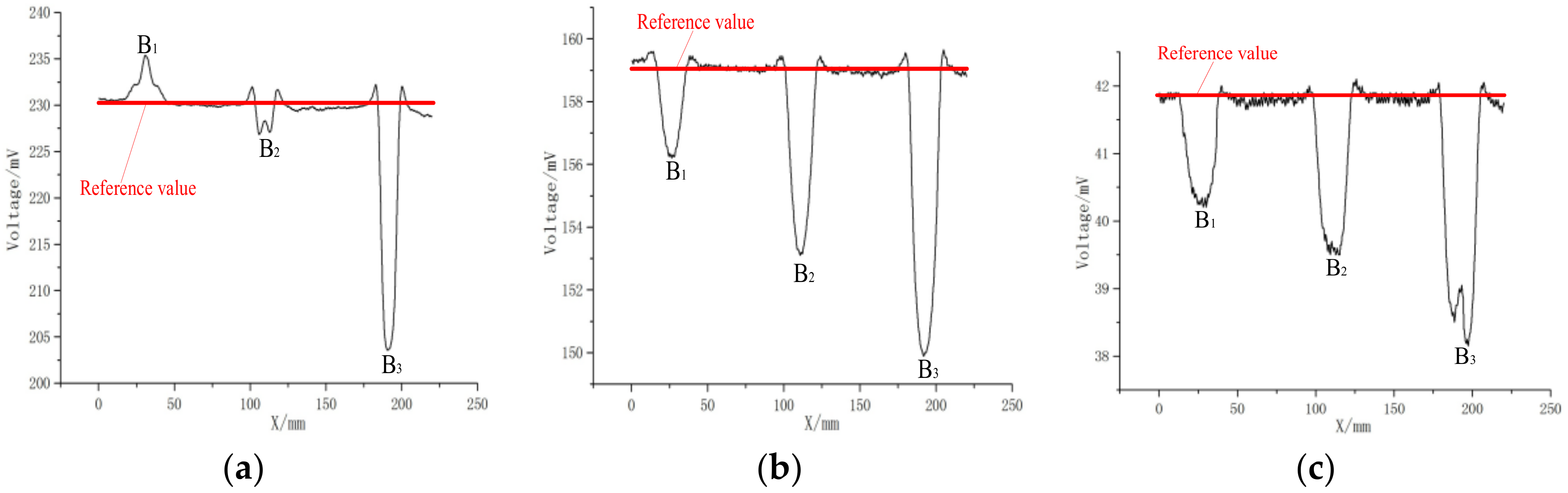
As shown in Figure 10, the non-conducting specimen (fiberglass board) contained three buried defects and the three buried defects from left to right were abbreviated to B1, B2 and B3. The diameters of these three defects were all 10mm and the buried depths of these three defects from left to right were 3 mm, 2 mm and 1 mm respectively. In addition, the distance between any two adjacent defects was 80 mm and the length of the line scans was 220 mm, leaving 20 mm on each side of the boundary to avoid edge effects. The red line shown in Figure 10 was the inspection path using the multi-electrode sensor and the lift-off was 0.1mm.
Through position compensation, the experimental results of the multi-electrode sensor detecting three buried defects were shown in Figure 11a–c. As shown in Figure 11a, the voltage of E21 detecting B1 was greater than the reference value which was rough red line. In previous work, the voltage would become greater when the conventional CI sensor defecting the defects on the surface of the conducting specimen. This abnormal phenomenon of detecting the non-conducting specimen was caused by the negative MSDs of different regions. Unlike the depths of the surface defects, it was extremely difficult to acquire approximately quantitative information about the depths of three buried defects because of the negative MSDs of different regions. If Figure 11a was the only picture acquired by the conventional CI sensor, B1 could be mistaken for a defect on the surface of the conducting specimen. As shown in Figure 11b,c the voltages of E31 and E41 detecting B1 were smaller than the corresponding reference values, which meant that B1 was a defect of the non-conducting specimen. By comparing these three line scans of B1, it could be sure that B1 was a defect of the non-conducting specimen, which could eliminate the misjudgment which was caused a single picture. Besides that, it was found that B1, B2 and B3 were the defects of the fiberglass board and their buried depths were decreased from left to right in turn. For B3 in Figure 11c, the two troughs were unequal, which was again caused by the MSDs asymmetry induced by the floating potential in actual experiments.
4.3. Defects within the Fiberglass Board and Aluminum Plate
As shown in Figure 12a, the insulator layer, which was fiberglass board, contained a buried defect. The diameter of this buried defect was 8 mm and the buried depth of the defect was 5 mm. As shown in Figure 12b, the conducting specimen, which was aluminum plate (grounded), contained a surface defect. The diameter of this surface defect was 8 mm and the depth of the defect was 5 mm. As shown in Figure 12c, the complete specimen was the aluminum plate covered by the fiberglass board. The horizontal distance between these two defects was 60 mm and the length of detecting path was 140 mm, leaving 45 mm on each side of the boundary to avoid edge effects. The red line shown in Figure 12c was the inspecting path using the multi-electrode sensor and the lift-off was 2 mm.
The voltage lines of E21, E31 and E41 obtained by using experimental system were shown in Figure 13a–c respectively. Comparing Figure 13a–c, the offset of any two adjacent electrode pairs (e.g., E21 and E31, E31 and E41), which was discussed in Figure 3b, was 6.5 mm. Through position compensation, the experimental DCRs of E21, E31 and E41 were shown in Figure 13d. The DCRs of the different electrode pairs detecting the center of two different kinds of defects presented different variation patterns, which were consistent with the simulation results. More narrowly, for the defect in the insulator layer, the DCRs of the center of the defect showed a monotonous decreasing trend with the electrode pairs changing from E21 to E31 to E41. While for the defect in the metal surface, the DCRs of the center of the defect showed a monotonous increasing trend with the electrode pairs changing from E21 to E31 to E41. Compared with the conventional CI sensor, the multi-electrode sensor could discriminate the defects in the insulation layer and metal surface by these different variation patterns. The two peaks of the DCRs of E31 and E41 detecting the defect in the insulator layer were roughly equal, because the ground aluminum plate weakened the MSDs asymmetry which was induced by the floating potential in actual experiments.
5. Discussions and Conclusions
In this paper, a new CI sensor with multiple electrodes was used to detect defects in the insulation layer and metal surface. The changes of the electric potential lines, which were acquired by FEM models, have validated the feasibility of multiple quasi-static electric fields detecting these defects. The MSDs of the multi-electrode sensor detecting the defects were acquired using the FEM models. The DCRs of the measured values obtained at the center of these two kinds of defects presented different variation patterns, which were verified by both FEM models and experiments. For the defect in the insulator layer, the DCRs of the measured values obtained at the center of the defect showed a monotonous decreasing trend with the electrode pairs changing from E21 to E31 to E41. While for the defect in the metal surface, the DCRs of the measured values obtained at the center of the defect showed a monotonous increasing trend with the electrode pairs changing from E21 to E31 to E41. These different variation patterns, which were explained by the trends of the changes of MSD, could be used to discriminate defects in the insulation layer and metal surface. In addition, analyzing all the detection results of the experiments can accurately compare the different depths of the defects in the insulator layer by using the multi-electrode sensor. For the surface defects, the surface depth was gradually decreasing from S1 to S2 to S3. Besides that, S1 and S2 were approximate with the sensing area of E31 and S3 was approximate with the sensing area of E21. For the buried defects, the buried depth was gradually decreasing from B1 to B2 to B3.
It should be noted that, based on the principle of electrostatic shielding, the quasi-static electric field from the CI probe cannot penetrate into a conducting surface. Therefore, when applied to pipe inspection, the CI method is only sensitive for defect in the insulation layer and the outer surface of the pipe. In future, the change rules of MSDs and DCRs of detecting the defects in the insulation layer and metal surface using the multi-electrode sensor will be further studied when the lift-off changes and the influence of different regions of the negative MSDs on detection results will be further analyzed.
Author Contributions
Writing-Original Draft Preparation, Z.L.; Investigation, Z.L and K.W.; Writing-Review & Editing, X.Y.; Visualization, Y.G.; Supervision, G.C.; Project Administration, W.L.; Funding Acquisition, X.Y and W.L.
Funding
This work was funded by the National Natural Science Foundation of China (No. 51675536 and No. 51574276), the Special national key research and development plan (No.2016YFC0802303), the Major National Science and Technology Program (2016ZX05028-001-05), the Fundamental Research Funds for the Central Universities (No.18CX02084A), the Applied Fundamental Research Fund of Qingdao (16-5-1-12-jch), the Shandong Provincial Natural Science Foundation, China (ZR2016EEQ26), the Postgraduate Innovation Project of China University of Petroleum (No.YCX2018056).
Conflicts of Interest
The authors declare no conflict of interest.
References
- Okamoto, K.; Maeda, T.; Haga, K. Dielectric property study of copper ionic migration at insulation layer on metal base PWB. J. Jpn. Inst. Interconnecting Packag. Electron. Circuits 2010, 12, 418–424. [Google Scholar] [CrossRef]
- Lizzit, S.; Larciprete, R.; Lacovig, P.; Dalmiglio, M.; Orlando, F.; Baraldi, A.; Gammelgaard, L.; Barreto, L.; Bianchi, M.; Perkins, E.; et al. Transfer-free electrical insulation of epitaxial graphene from its metal substrate. Nano Lett. 2012, 12, 4503–4507. [Google Scholar] [CrossRef] [PubMed]
- Al-Sanea, S.A.; Zedan, M.F. Improving thermal performance of building walls by optimizing insulation layer distribution and thickness for same thermal mass. Appl. Energy 2011, 88, 3113–3124. [Google Scholar] [CrossRef]
- Jiang, Y.; Liu, M.; Zhang, W.; Lan, W.; Gai, J.; Ren, A.; Jiang, Y. Corrosion survey for field joints of long-distance thermal insulated pipeline. Corros. Sci. Prot. Technol. 2017, 29, 323–327. [Google Scholar]
- Zhang, Y.M.; Tan, T.K.; Xiao, Z.M.; Zhang, W.G.; Ariffin, M.Z. Failure assessment on offshore girth welded pipelines due to corrosion defects. Fatigue Fract. Eng. Mater. Struct. 2016, 39, 453–466. [Google Scholar] [CrossRef]
- Eibach, S.; Moes, G.; Hou, Y.J.; Zovickian, J.; Pang, D. Unjoined primary and secondary neural tubes: Junctional neural tube defect, a new form of spinal dysraphism caused by disturbance of junctional neurulation. Child’s Nerv. Syst. 2016, 33, 1–15. [Google Scholar] [CrossRef] [PubMed]
- Tan, M.Y.J.; Varela, F.; Huo, Y.; Mahdavi, F.; Forsyth, M.; Hinton, B. New electrochemical methods for visualizing dynamic corrosion and coating disbondment processes on simulated pipeline conditions. Corros. Mater. 2017, 42, 70–74. [Google Scholar]
- Nazir, H.; Khan, Z.; Saeed, A. A novel non-destructive sensing technology for on-site corrosion failure evaluation of coatings. IEEE Access 2018, 6, 1042–1045. [Google Scholar] [CrossRef]
- Liu, Y.; Pei, S.; Fu, W.; Zhang, K.; Ji, X.; Yin, Z. The discrimination method as applied to a deteriorated porcelain insulator used in transmission lines on the basis of a convolution neural network. IEEE Trans. Dielectr. Electr. Insul. 2018, 24, 3559–3566. [Google Scholar] [CrossRef]
- Yin, X.; Hutchins, D.A. Non-destructive evaluation of composite materials using a capacitive imaging technique. Compos. Part B 2012, 43, 1282–1292. [Google Scholar] [CrossRef]
- Yin, X.; Hutchins, D.A.; Diamond, G.G.; Purnell, P. Non-destructive evaluation of concrete using a capacitive imaging technique: Preliminary modelling and experiments. Cem. Concr. Res. 2010, 40, 1734–1743. [Google Scholar] [CrossRef] [Green Version]
- Yin, X.; Hutchins, D.A.; Chen, G.; Li, W.; Xu, Z. Studies of the factors influencing the imaging performance of the capacitive imaging technique. NDT & E Intern. 2013, 60, 1–10. [Google Scholar] [CrossRef]
- Yin, X.; Hutchins, D.; Hutchins, D.A.; Chen, G.; Li, W. Investigations into the measurement sensitivity distribution of coplanar capacitive imaging probes. NDT & E Intern. 2013, 58, 1–9. [Google Scholar] [CrossRef]
- Yang, W.Q.; Stott, A.L.; Beck, M.S.; Xie, C.G. Development of capacitance tomographic imaging systems for oil pipeline measurements. Rev. Sci. Instrum. 1995, 66, 4326–4332. [Google Scholar] [CrossRef]
- Meribout, M.; Saied, I.M. Real-time two-dimensional imaging of solid contaminants in gas pipelines using an electrical capacitance tomography system. IEEE Trans. Ind. Electron. 2017, 64, 3989–3996. [Google Scholar] [CrossRef]
- Martin, R.; Ortiz-Alemán, C.; Rodríguez Castellanos, A. Multiphase flow reconstruction in oil pipelines by capacitance tomography using simulated annealing. Geofísica Internacional 2015, 44, 241–250. [Google Scholar]
- Montalvo, C.; García-Berrocal, A.; Blázquez, J.; Balbás, M. Application of the monte carlo method for capacitive pressure transmitters surveillance in nuclear power plants. J. Dyn. Syst. Meas. Contr. 2012, 134, 1338–1343. [Google Scholar] [CrossRef]
- Mariani, A.; Blacka, M.J.; Cox, R.J.; Coghlan, I.R.; Carley, J.T. Wave overtopping of coastal structures. physical model versus desktop predictions. J. Coastal Res. 2009, 25, 534–538. [Google Scholar]
- Cassani, D. Existence and non-existence of solitary waves for the critical Klein–Gordon equation coupled with Maxwell’s equations. Nonlinear Anal. Theory Methods Appl. 2017, 58, 733–747. [Google Scholar] [CrossRef]
- Collinson, G.; Mitchell, D.; Xu, S.; Glocer, A.; Grebowsky, J.; Hara, T.; Lillis, R.; Espley, J.; Mazelle, C.; Sauvaud, J.-A.; et al. Electric Mars: A large trans-terminator electric potential drop on closed magnetic field lines above Utopia Planitia. J. Geophys. Res. Space Phys. 2017, 122, 2260–2271. [Google Scholar] [CrossRef]
- Helsdon, J.H., Jr.; Gattaleeradapan, S.; Farley, R.D.; Waits, C.C. An examination of the convective charging hypothesis: Charge structure, electric fields and Maxwell currents. J. Geophys. Res. 2002, 107, 9–26. [Google Scholar] [CrossRef]
- Peng, J.; Wu, Y.; Qiu, J.; Ji, H.; Wang, Y. Development and test of multi-channel charge amplifier based on ARM. Piezoelecs. & Acoustoptcs. 2017, 39, 211–215. [Google Scholar]
- Sasao, T.; Nagayama, S.; Butler, J.T. Numerical function generators using LUT cascades. IEEE Trans. Comput. 2007, 56, 826–838. [Google Scholar] [CrossRef]
- Carminati, M.; Gervasoni, G.; Sampietro, M.; Ferrari, G. Note: Differential configurations for the mitigation of slow fluctuations limiting the resolution of digital lock-in amplifiers. Rev. Sci. Instrum. 2016, 87, 296–297. [Google Scholar] [CrossRef] [PubMed]
- Kong, J.; Su, H.; Chen, Z.-Q.; Dong, C.-F.; Qian, Y.; Gao, S.-S.; Zhou, C.-Y.; Lu, W.; Ye, R.-P.; Ma, J.-B. Development of multi-channel gated integrator and PXI-DAQ system for nuclear detector arrays. Nucl. Instrum. Methods Phys. Res. Sect. A 2010, 622, 215–218. [Google Scholar] [CrossRef]
Figure 1.
Detection principle of CI: (a) CI sensor inspecting the non-conducting specimen; (b) CI sensor inspecting the conducting specimen covered by an insulation layer; CI: capacitive imaging.
Figure 1.
Detection principle of CI: (a) CI sensor inspecting the non-conducting specimen; (b) CI sensor inspecting the conducting specimen covered by an insulation layer; CI: capacitive imaging.

Figure 2.
Detection principle of the multi-electrode sensor: (a) the multi-electrode sensor inspecting the non-conducting specimen; (b) the multi-electrode sensor inspecting the conducting specimen covered by an insulation layer.
Figure 2.
Detection principle of the multi-electrode sensor: (a) the multi-electrode sensor inspecting the non-conducting specimen; (b) the multi-electrode sensor inspecting the conducting specimen covered by an insulation layer.

Figure 3.
(a) the front view of the multi-electrode sensor, (b) the cross-section of the multi-electrode sensor and (c) the multi-electrode sensor inspecting the conducting specimen covered by the insulation layer.
Figure 3.
(a) the front view of the multi-electrode sensor, (b) the cross-section of the multi-electrode sensor and (c) the multi-electrode sensor inspecting the conducting specimen covered by the insulation layer.
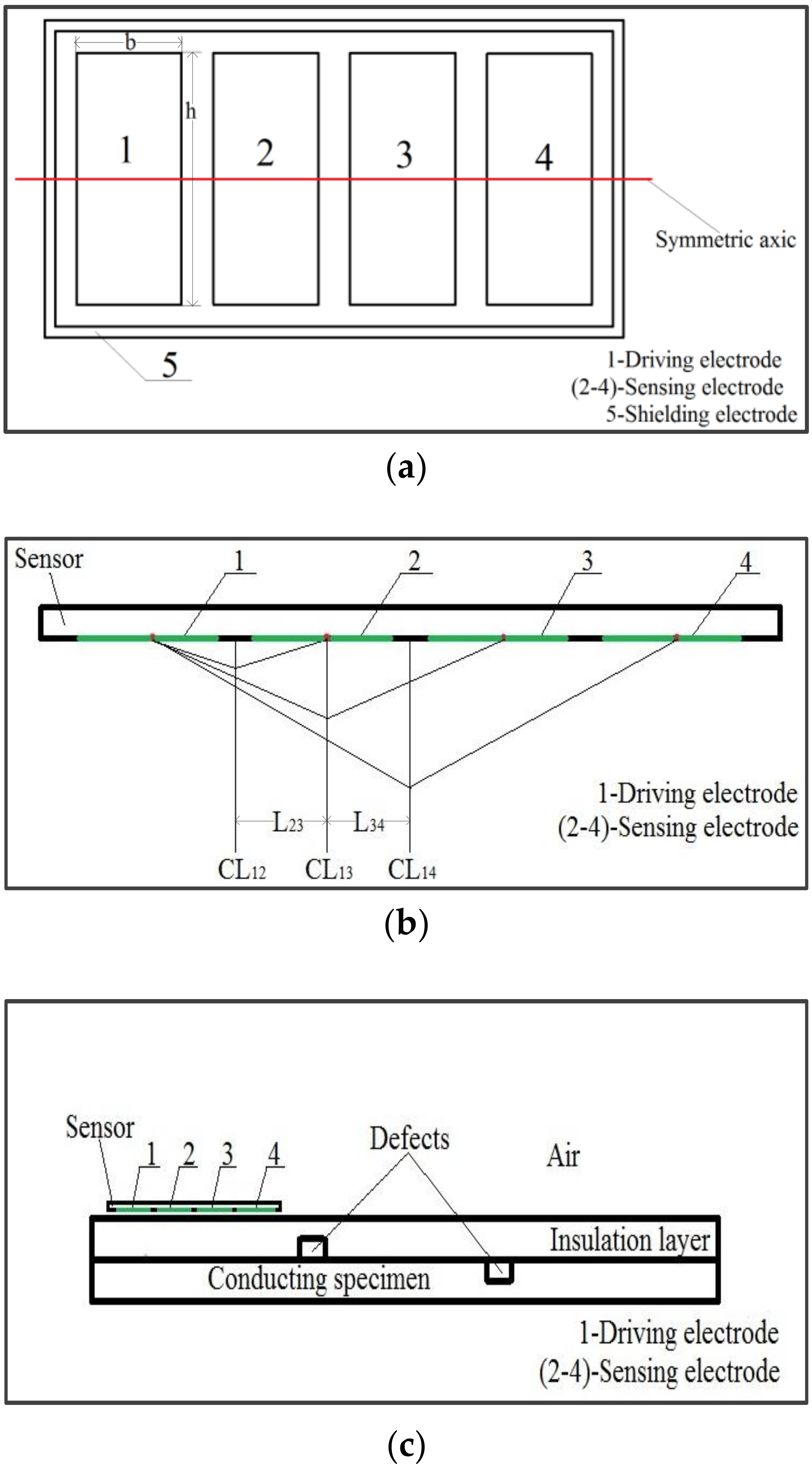
Figure 4.
Electric potential diagrams of the multi-electrode sensor: (a) sensor inspecting the specimen without defects, (b) sensor inspecting a defect located in the insulation layer and (c) sensor inspecting a defect located on the surface of the conducting specimen.
Figure 4.
Electric potential diagrams of the multi-electrode sensor: (a) sensor inspecting the specimen without defects, (b) sensor inspecting a defect located in the insulation layer and (c) sensor inspecting a defect located on the surface of the conducting specimen.
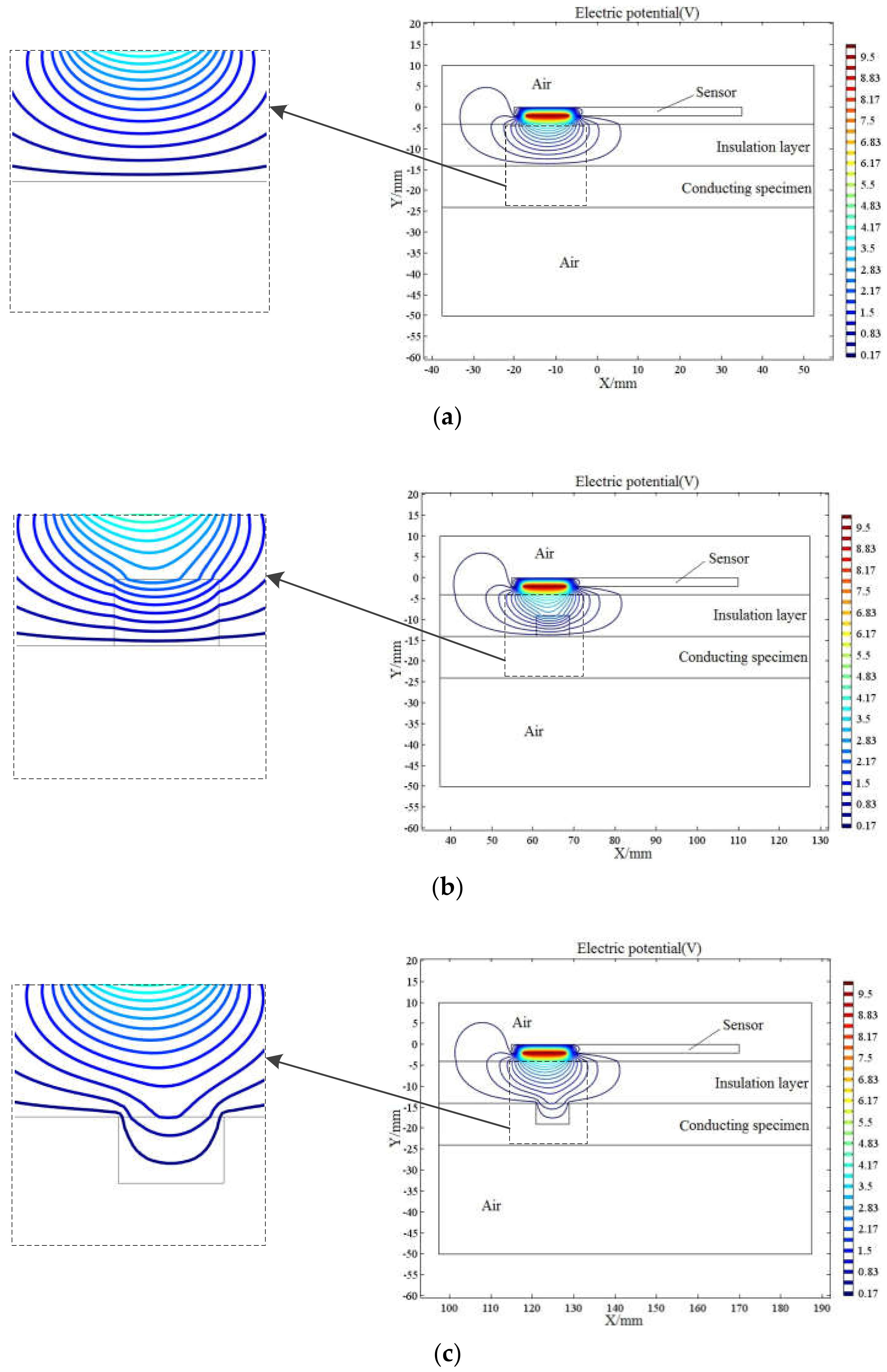
Figure 5.
Measurement Sensitivity Distribution (MSD) diagrams of the multi-electrode sensor: E21 inspecting the specimen without defects (a), the defect located in the insulation layer (b) and the defect located on the surface of the conducting specimen (c); E31 inspecting the specimen without defects (d), the defect located in the insulation layer (e) and the defect located on the surface of the conducting specimen (f); E41 inspecting the specimen without defects (g), the defect located in the insulation layer (h) and the defect located on the surface of the conducting specimen (i).

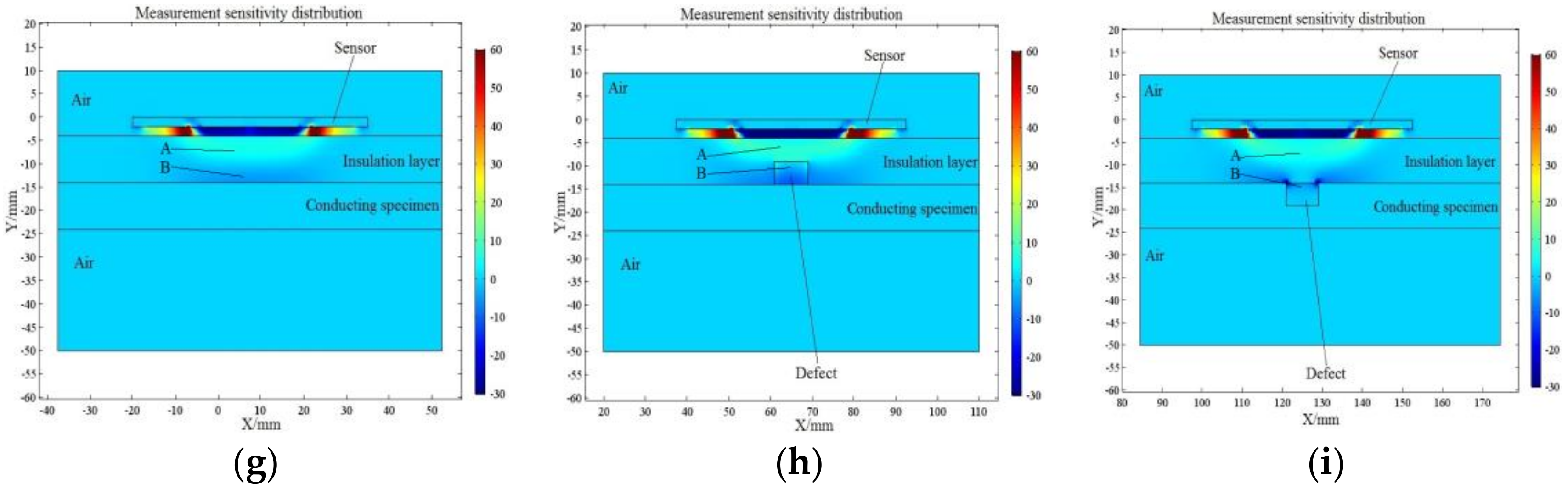
Figure 6.
Test results: (a) the capacitances of E21, (b) the capacitances of E31, (c) the capacitances of E41, (d) the DCRs of E21, E31 and E41; DCRs: Dynamic Change Rates.
Figure 6.
Test results: (a) the capacitances of E21, (b) the capacitances of E31, (c) the capacitances of E41, (d) the DCRs of E21, E31 and E41; DCRs: Dynamic Change Rates.
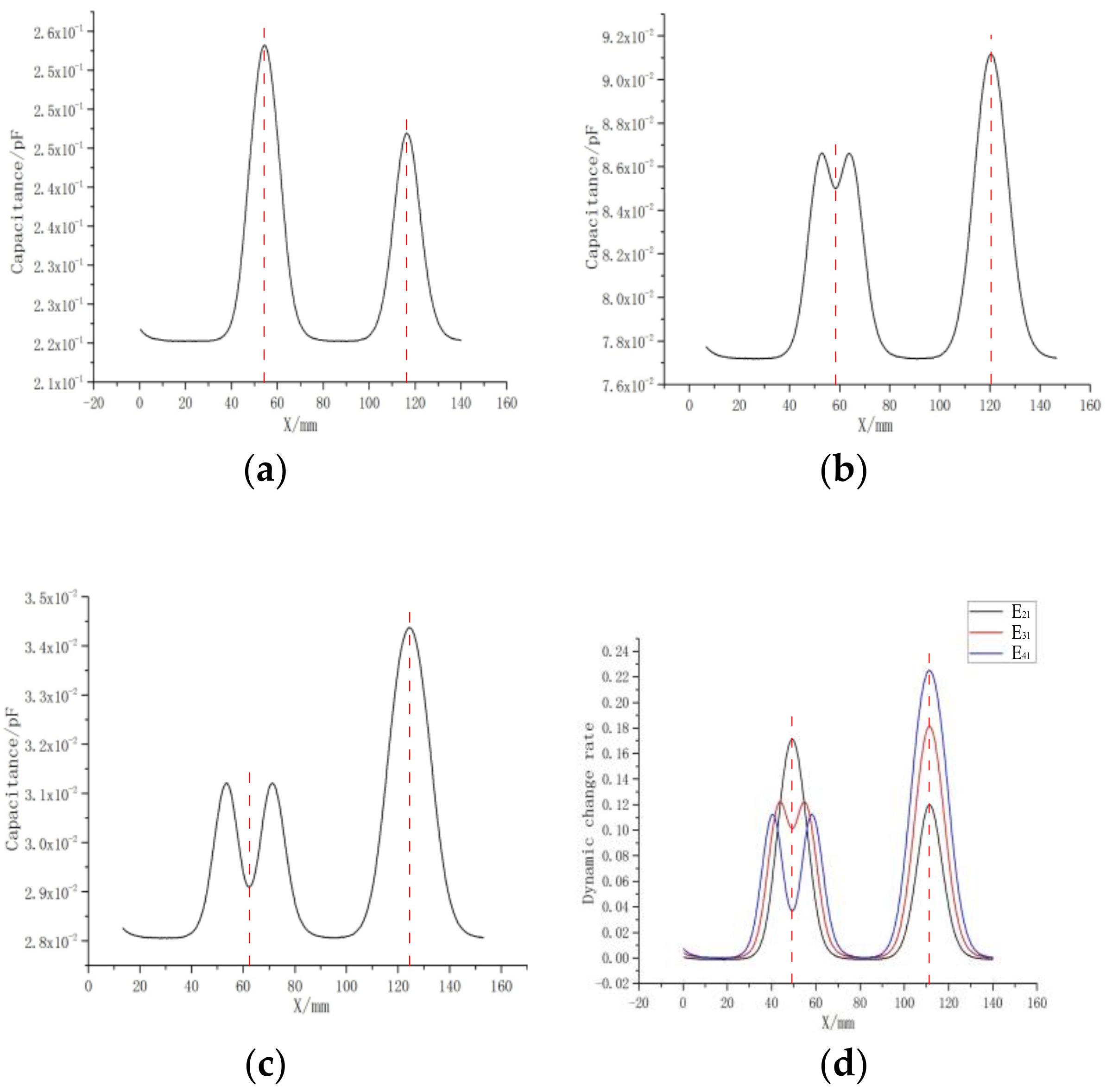
Figure 7.
Setup of basic experimental system.
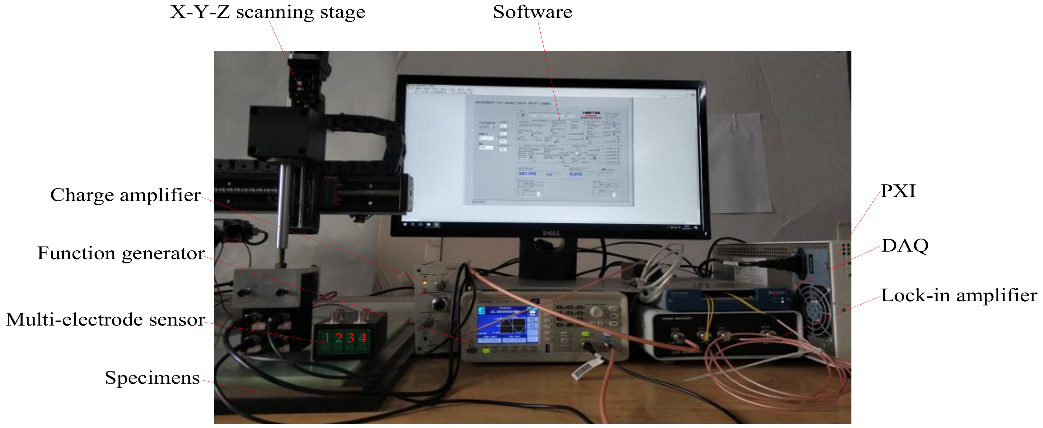
Figure 8.
Schematic diagram of a 12 mm thick fiberglass board containing flat bottomed holes of surface depth (from left to right) 3 mm, 2 mm and 1 mm.
Figure 8.
Schematic diagram of a 12 mm thick fiberglass board containing flat bottomed holes of surface depth (from left to right) 3 mm, 2 mm and 1 mm.

Figure 9.
The signal strength diagrams with the multi-electrode sensor with 0.1mm lift-off: (a) E21, (b) E31, (c) E41.
Figure 9.
The signal strength diagrams with the multi-electrode sensor with 0.1mm lift-off: (a) E21, (b) E31, (c) E41.
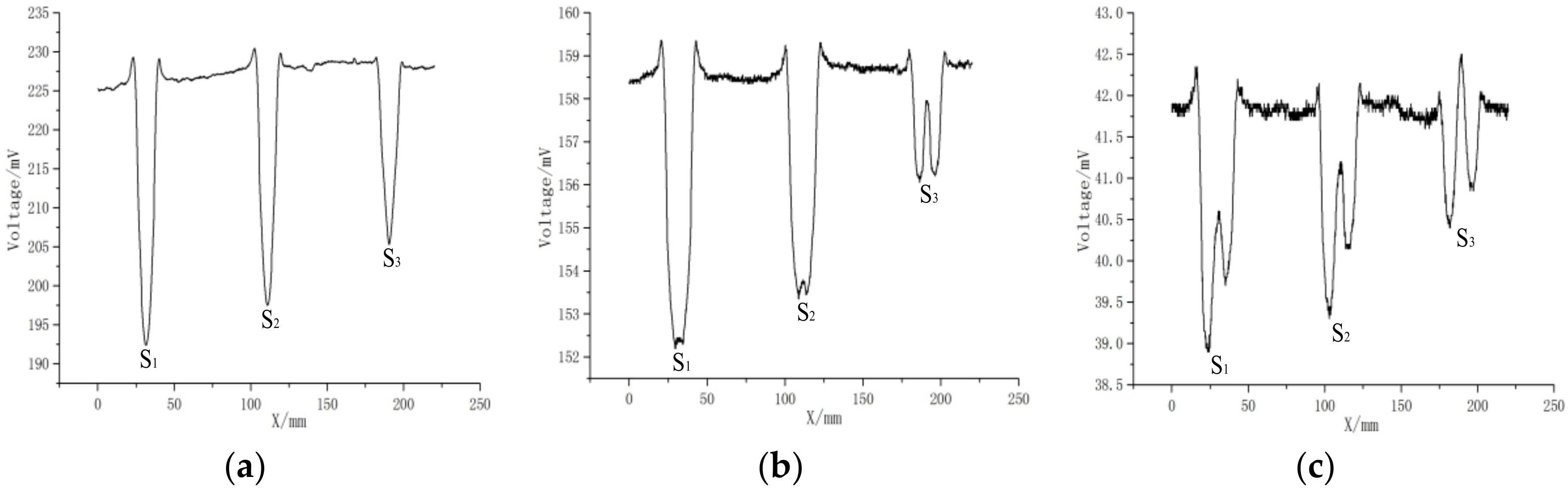
Figure 10.
Schematic diagram of a 12 mm thick fiberglass board containing flat bottomed holes of buried depth (from left to right) 3 mm, 2 mm and 1 mm.
Figure 10.
Schematic diagram of a 12 mm thick fiberglass board containing flat bottomed holes of buried depth (from left to right) 3 mm, 2 mm and 1 mm.
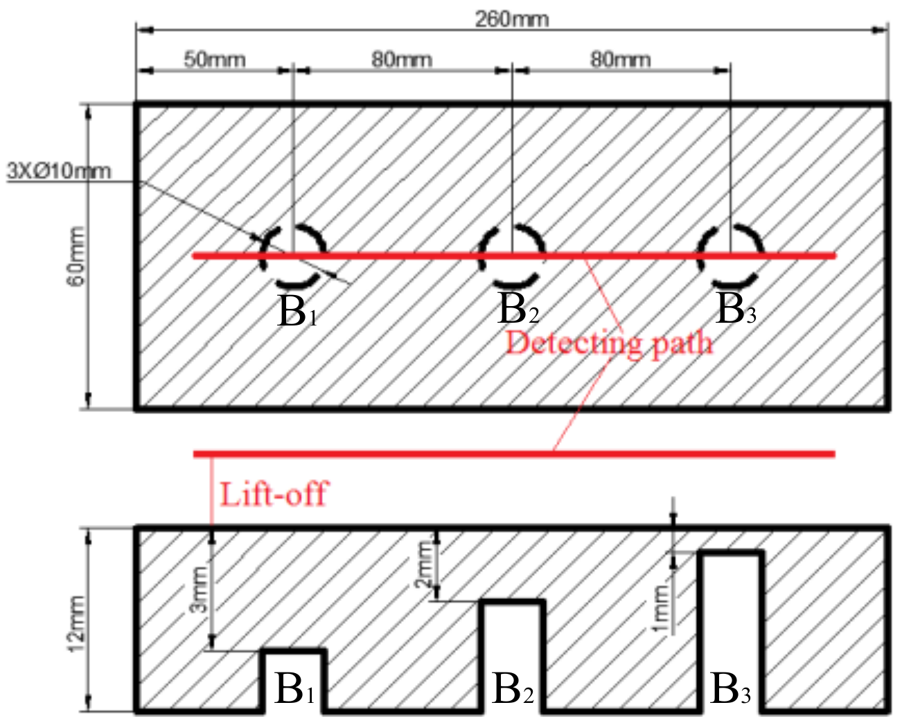
Figure 11.
The signal strength diagrams with the multi-electrode sensor with 0.1 mm lift-off: (a) E21, (b) E31, (c) E41.
Figure 11.
The signal strength diagrams with the multi-electrode sensor with 0.1 mm lift-off: (a) E21, (b) E31, (c) E41.

Figure 12.
Schematic diagram of insulator layer and conducting specimen: (a) insulator layer, (b) conducting specimen, (c) conducting specimen covered by insulator layer.
Figure 12.
Schematic diagram of insulator layer and conducting specimen: (a) insulator layer, (b) conducting specimen, (c) conducting specimen covered by insulator layer.

Figure 13.
Experimental results: (a) the voltages of E21, (b) the voltages of E31, (c) the voltages of E41, (d) the DCRs of E21, E31 and E41.The dynamic change rate of E21, E31 and E41.
Figure 13.
Experimental results: (a) the voltages of E21, (b) the voltages of E31, (c) the voltages of E41, (d) the DCRs of E21, E31 and E41.The dynamic change rate of E21, E31 and E41.

© 2018 by the authors. Licensee MDPI, Basel, Switzerland. This article is an open access article distributed under the terms and conditions of the Creative Commons Attribution (CC BY) license (http://creativecommons.org/licenses/by/4.0/).
Share and Cite
MDPI and ACS Style
Li, Z.; Chen, G.; Gu, Y.; Wang, K.; Li, W.; Yin, X. Further Investigations into the Capacitive Imaging Technique Using a Multi-Electrode Sensor. Appl. Sci. 2018, 8, 2296. https://doi.org/10.3390/app8112296
AMA Style
Li Z, Chen G, Gu Y, Wang K, Li W, Yin X. Further Investigations into the Capacitive Imaging Technique Using a Multi-Electrode Sensor. Applied Sciences. 2018; 8(11):2296. https://doi.org/10.3390/app8112296
Chicago/Turabian StyleLi, Zhen, Guoming Chen, Yue Gu, Kefan Wang, Wei Li, and Xiaokang Yin. 2018. "Further Investigations into the Capacitive Imaging Technique Using a Multi-Electrode Sensor" Applied Sciences 8, no. 11: 2296. https://doi.org/10.3390/app8112296
Note that from the first issue of 2016, this journal uses article numbers instead of page numbers. See further details here.