1. Introduction
Gallium Nitride (GaN) is widely used for wireless telecommunications and radar systems because of its superior material and electronic properties, such as wide bandgap (3.4 eV) and high breakdown field (2–3.3 MV/cm) [
1,
2,
3]. These characteristics make GaN more practicable for high-voltage and high-temperature applications than many other materials, such as silicon or gallium arsenide [
4]. Similarly, high electron mobility transistors (HEMTs) based on the AlGaN/GaN heterostructure show excellent performance owing to the two-dimensional electron gas (2-DEG) in the channel region. As a consequence of spontaneous and piezoelectric polarization effects, the 2-DEG shows high carrier mobility and high saturation velocity, which have important roles in the output current and power amplification [
5,
6]. Nevertheless, HEMTs need to be improved to fully cater to the market requirements [
7].
For class A HEMT operation [
8,
9,
10], the AC maximum power (P) is described in Equation (1),
where the gap between the knee and breakdown voltages determines
, and the maximum current defines
. Hence, low knee voltage, high off-state breakdown voltage, and high maximum current are very important features to improve the device performance of HEMTs.
Generally, the field plate (FP) technology has been exploited to increase the breakdown voltage of AlGaN/GaN HEMTs and has been applied to millimeter wave frequencies for many purposes [
11,
12,
13]. However, the FP gate structure produces additional gate capacitance and also increases the gate-to-source capacitance (
) and gate-to-drain capacitance (
). These increased parasitic capacitances degrade the radio frequency (RF) performance at higher frequency operations and also reduce the power efficiency in the operational frequency range. Some groups have already studied the gate-head design modeling to improve the direct current (DC) and RF performance of AlGaN/GaN HEMTs [
14,
15,
16]. Particularly, gamma-shaped, camel-shaped, and T-shaped gates are a few examples where a metal FP is connected to the gate electrode for optimum results [
17,
18,
19]. These gate-head structures have been reported to exploit the versatility and high performance of GaN-based FP HEMTs [
20]. The device performs differently as the FP is moved from the source-side edge to the drain-side edge of the device. Hence, the most appropriate results for transconductance, output current, and breakdown voltage are achieved by the T-shaped gate structure for high-power applications. AlGaN/GaN HEMTs using a dual-gate structure are proposed to modulate the threshold voltage without employing any special fabrication techniques such as plasma treatment, recessed gate-head structure, and the addition of a p-GaN gate layer [
21]. Also, a floating gate is embedded between the control gate and drain electrode to improve the DC characteristics with low leakage current, high on/off ratio, and breakdown voltage [
22]. However, the systematic optimization of dual-gate structures has not been reported for high-power and high-frequency operations.
In this study, to analyze the DC characteristics, conventional T-shaped gate AlGaN/GaN HEMTs were simulated, and the fabricated two-finger device was characterized for clarity. For more accuracy, the electrical parameters were fixed, and the simulation was performed. On the basis of the conventional T-shaped gate structure, the fabricated and simulated data were first compared and contrasted. Then, the optimized device structure, with best possible electrical characteristics obtained by changing the geometry of the FP structure, was investigated using technology computer aided design (TCAD) simulations. The drain-side FP structure was characterized to boost the breakdown voltage, and the optimum FP length point was identified for the highest breakdown voltage. Finally, an inner field-plate (IFP) structure was adopted to compensate the degradation of the RF characteristics caused by the FP structure. The optimum gate end-point of the FP structure was chosen and fixed to be taken as the starting point for the IFP structure. Then, the IFP structure was extended from that starting point toward the gate direction to analyze the variations of the cut-off frequency () and maximum frequency () with minimum loss in breakdown voltage. Consequently, we propose an optimum IFP construction for AlGaN/GaN HEMTs with enhanced breakdown voltage and RF characteristics.
2. Materials and Methods
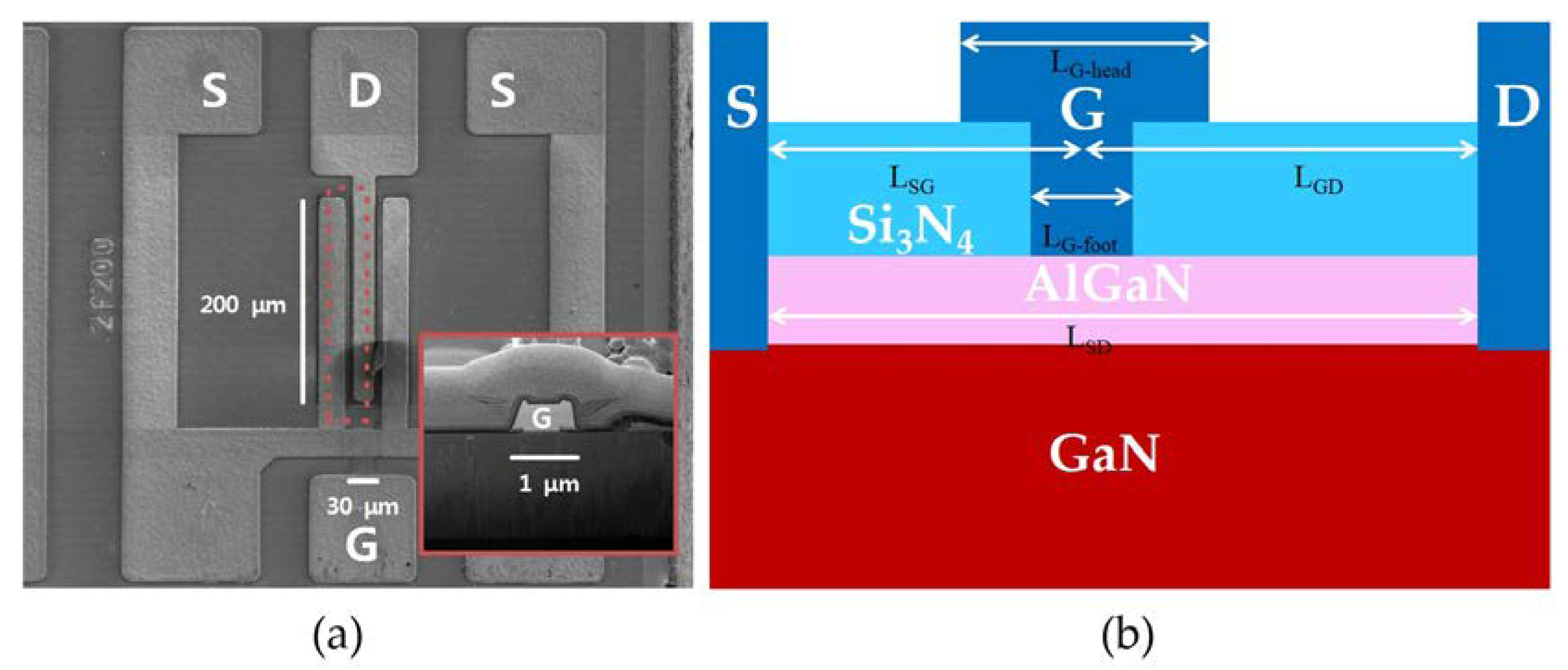
Figure 1a shows the top view of a fabricated two-finger AlGaN/GaN HEMT. The extension of the gate structure is provided with a lower square contacting pad (G), and the center upper pad is a drain electrode (D). The drain electrode is enclosed between two source electrodes (S). The inset is a magnified cross-sectional SEM image of the dotted region showing the conventional T-shaped gate structure. The AlGaN/GaN heterostructure was grown on a (111) silicon substrate by metal-organic chemical vapor deposition. It consists of a 2-μm-thick acceptor-doped GaN buffer layer, a 100-nm-thick i-GaN layer, and a 25-nm-thick i-AlGaN barrier layer with a nominal 25% Al composition. Because of a large lattice mismatch and thermal expansion coefficient between Si and the AlGaN/GaN layer, a C-doped GaN buffer was employed as an insertion layer. To fabricate AlGaN/GaN HEMTs, a 200-nm-thick mesa isolation was performed by Cl
2/BCl
3-based inductively coupled plasma reactive-ion etching (ICP RIE). The AlGaN/GaN mesa etching was performed at a flow rate of 18/3 sccm for the Cl
2/BCl
3, a process pressure of 5 mTorr, an RF power of 100 W, and an ICP power of 300 W. The source and drain ohmic contacts were made by evaporating Ti/Al/Ti/Ni/Au (30/150/20/30/100 nm) metal stack via e-beam metal evaporation. A Ti/Al-based structure was used as diffusion layer to form TiN or AlTi
2N layers, and the Ti/Ni layers were used as diffusion barriers for Au in the following rapid thermal annealing process. The rapid thermal annealing temperature was 400
for 150 s, 700
for 30 s, and 820
for 30 s. The measured values of specific contact resistivity and sheet resistance were 5.2 × 10
−6 Ω·cm
2 and ~700 Ω/□, respectively. A 50-nm-thick protective Si
3N
4 passivation film was deposited via plasma-enhanced chemical vapor deposition (PECVD) at a deposition rate of 150 Å/min. The conditions were: SiH
4/NH
3/He of 2.8/8/80 sccm, a pressure of 35 mTorr, an RF power of 100 W, and a substrate temperature of 250 °C. To expose the AlGaN layer surface, an etching window was opened with photolithography, and the Si
3N
4 was etched using a CF
4/O
2-based ICP RIE process at CF
4/O
2 condition of 110/5 sccm, a pressure of 45 mTorr, and an RF power of 100 W. The etch rate was 110 Å/min. Afterward, a Ni/Au (40/100 nm) Schottky gate electrode was fabricated by photolithography followed by e-beam metal evaporation. Finally, the T-shaped gate was formed on the Si
3N
4 passivation layer. Similarly, a second Si
3N
4 passivation layer was deposited using PECVD at the same above-mentioned deposition and etching conditions, followed by the contact pad opening. To ensure data reliability, a cross-sectional schematic of a basic device structure is shown in
Figure 1b. The unit device structure of one-finger was used in the modeling. Other geometrical parameters of the device are listed in
Table 1. For convenience, FP length, gate foot length, gate head length, source gate length, gate drain length, and source drain length are designated as L
FP, L
G-foot, L
G-head, L
SG, L
GD, and L
SD, respectively.
The imbibed wurtzite structure of AlGaN/GaN heterostructures produces polarization in the device. Piezoelectric and spontaneous polarizations form a 2-DEG in the channel region via tensile and compressive stresses. Therefore, the modeling factors, such as polarization effect, energy bandgap, electron affinity, relative permittivity, mobility, saturation velocity, and Shockely–Read–Hall (SRH) recombination with fixed carrier lifetimes should be carefully considered, as presented in
Table 2. The electron velocity is saturated in the 2-DEG region with a significant increase in electric field. This effect is because of a reduction in the effective mobility, since the magnitude of the drift velocity is the product of the mobility and the electric field. Therefore, a GaN-based saturation velocity model was used to find out the value of electron mobility (
) as a function of applied parallel electric field (
), as denoted in Equation (2),
where
and VSATN are electron low-field mobility and saturation velocity, respectively, and N1N·GANSAT, ECN·GANSAT, ANN·GANSAT, and N2N·GANSAT are fitting parameters which were calculated with Monte Carlo methods [
23,
24]. Furthermore, the Selberherr model was used to calculate the impact ionization process near the gate edge of the device [
25,
26].
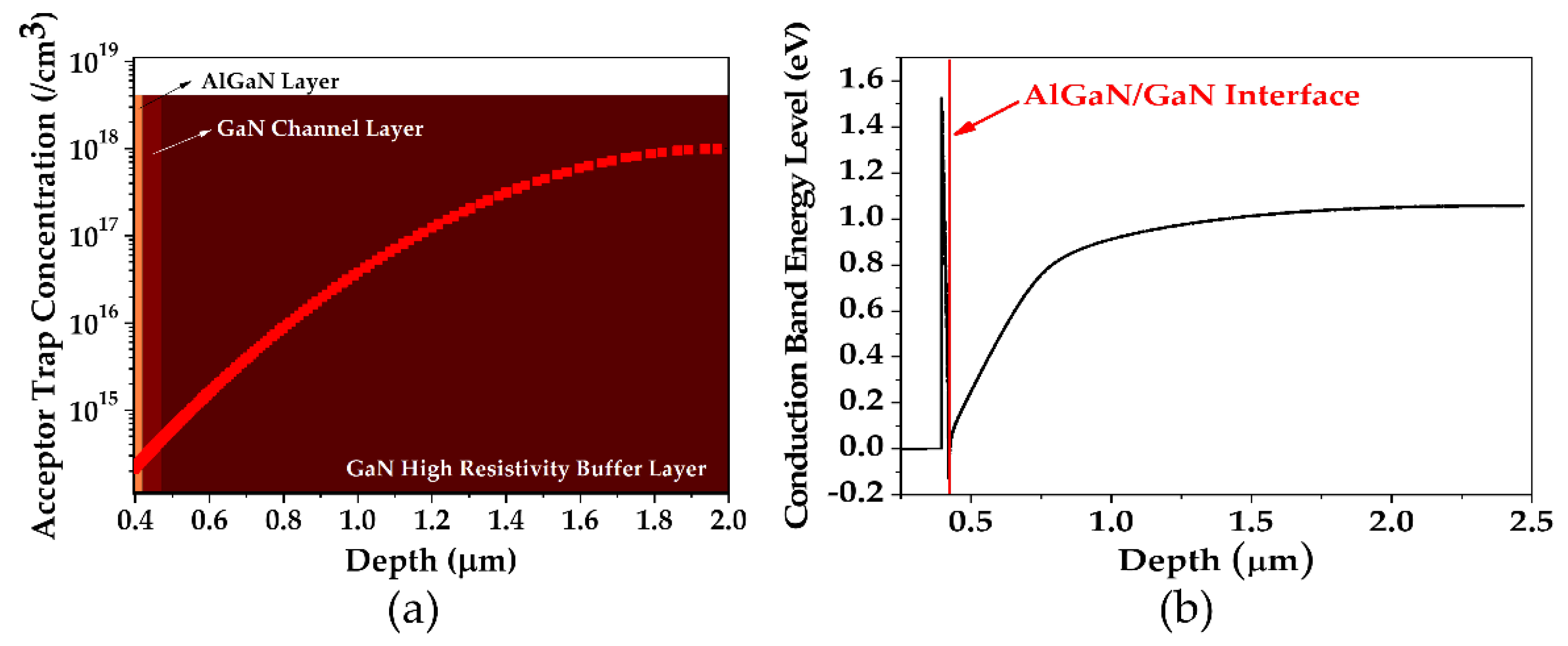
Figure 2 shows the overall characteristics of acceptor doping in the GaN buffer layer. Acceptor traps were exploited to minimize the electron punch-through effect via the GaN buffer layer, and the exact concentration of acceptor traps is shown in
Figure 2a. The peak trap concentration was ~10
18/cm
3, where the doping concentration was reduced to below 10
15/cm
3 at the AlGaN/GaN interface for higher carrier density in the 2-DEG channel layer. The conduction band energy level of the simulated device is presented in
Figure 2b. The acceptor doping increased the conduction band energy of the GaN buffer layer, which improved the breakdown characteristics of the HEMT via an electron confinement effect.
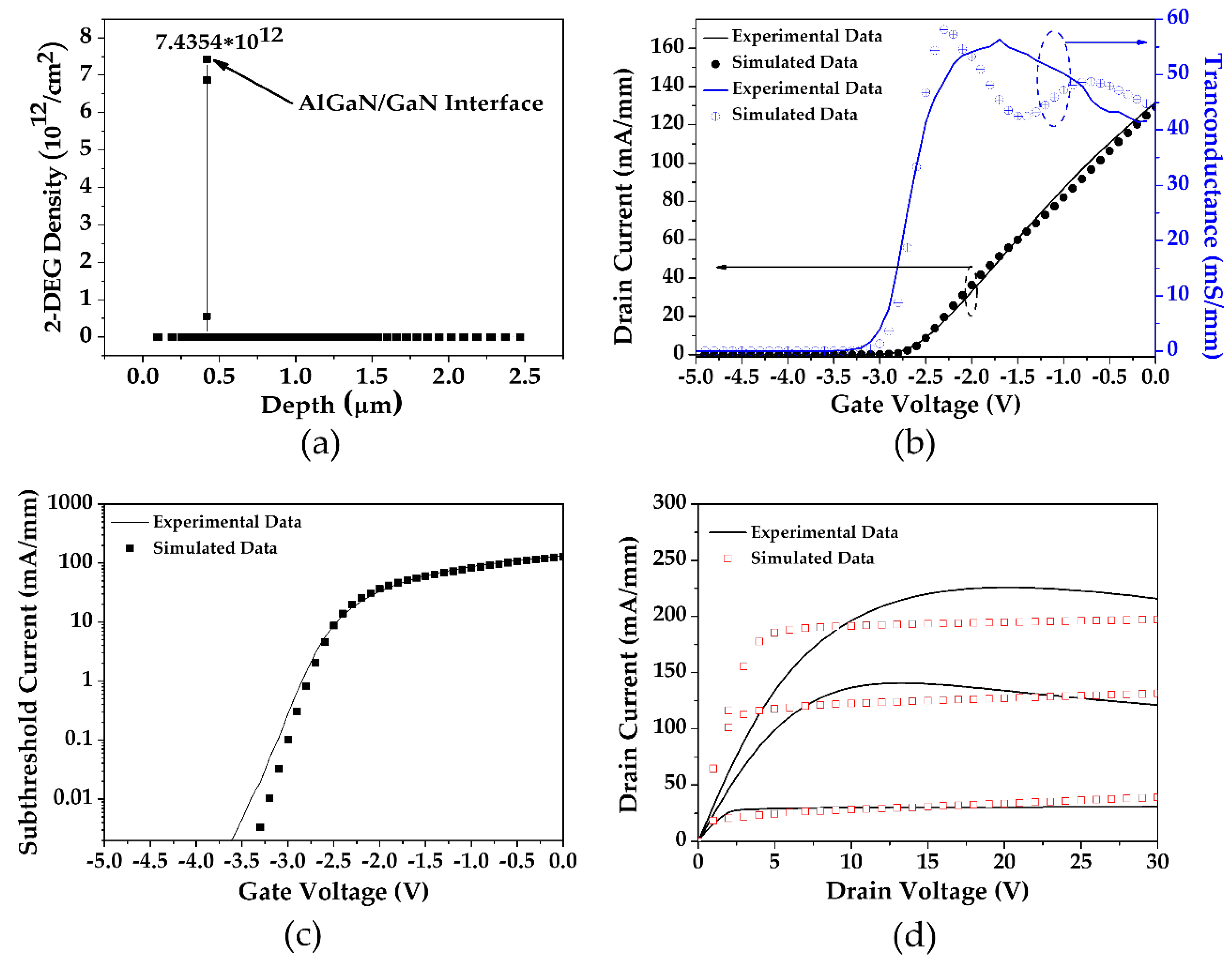
Figure 3 presents the electrical characteristics of the simulated device. The 2-DEG charge density based on spontaneous and piezoelectric polarizations is presented in
Figure 3a. The 2-DEG charge carrier density at the AlGaN/GaN interface was
/cm
2.
Figure 3b shows the threshold voltage (V
th) and transconductance (g
m) of the measured and simulated T-shaped gate AlGaN/GaN HEMTs, where the basic structures of both devices are already portrayed in
Figure 1a,b. The drain current and transfer characteristics of the HEMTs were measured at room temperature using a Yokogawa GS200 and Keithley 2410 DC bias measurement systems in a probe station. Equation (3) describes the threshold voltage (V
th) in the modeling as:
where
,
,
,
,
, and
are Schottky barrier height, conduction band difference between GaN and AlGaN, electron charge, 2-DEG density, AlGaN layer thickness, and AlGaN relative dielectric constant, respectively. Hence, it is inferred that the work function of the gate material, the 2-DEG concentration controlled by Al mole fraction, and the AlGaN thickness are important parameters to control the
of the device. Both simulated and experimental devices show typical normally-on HEMT characteristics, with a negative
and similar tendencies. The channel region disappears when the gate voltage is reduced below
. A linear fitting method was applied to determine
in
Figure 3b. The simulated
value was −2.683 V, with a subthreshold current of 2.504 mA/mm, which almost matched the experimental value of −2.643 V, with a subthreshold current of 4.457 mA/mm. The measured and simulated values of peak
were 57 and 58 mS/mm at −1.7 and −2.15 V, respectively.
Figure 3c shows the drain leakage current as a function of the gate voltage in log scale. The GaN buffer layer doping profile directly controls the subthreshold swing and threshold voltage of the device. Thus, the GaN buffer layer doping profile was judiciously adjusted for better device characteristics. The subthreshold current of the simulated device was well matched with the experimental device. The drain–source saturation current (
) is shown in
Figure 3d. The gate voltages were 2, 0, and −2 V from the top drain–current curve, and the drain voltage step was 1 V. The knee voltage of the fabricated device was higher than that of the simulated one, as shown in
Figure 3d. Also, thermal degradation was found when the drain voltage was higher than 15 V. The thermal parameters were not considered for the simulated devices. Hence, the
appears almost parallel to the
x-axis. Nevertheless, the measured and simulated current values were almost similar and found in accordance to each other. All the simulated discussions were progressed from the device with the aforementioned electrical characteristics.
3. Results and Discussion
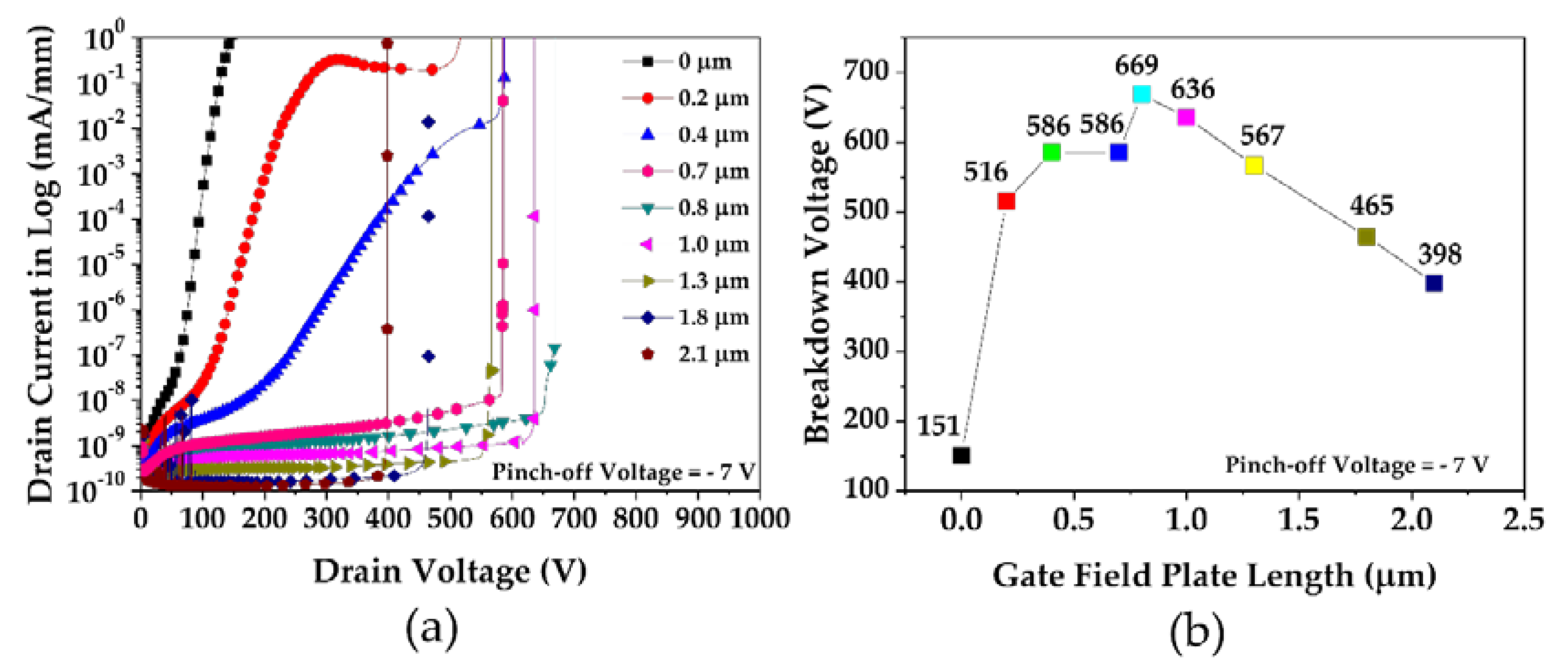
On the basis of the conventional T-shaped gate structure, the DC characteristics of the device were analyzed by changing the geometry of the FP structure.
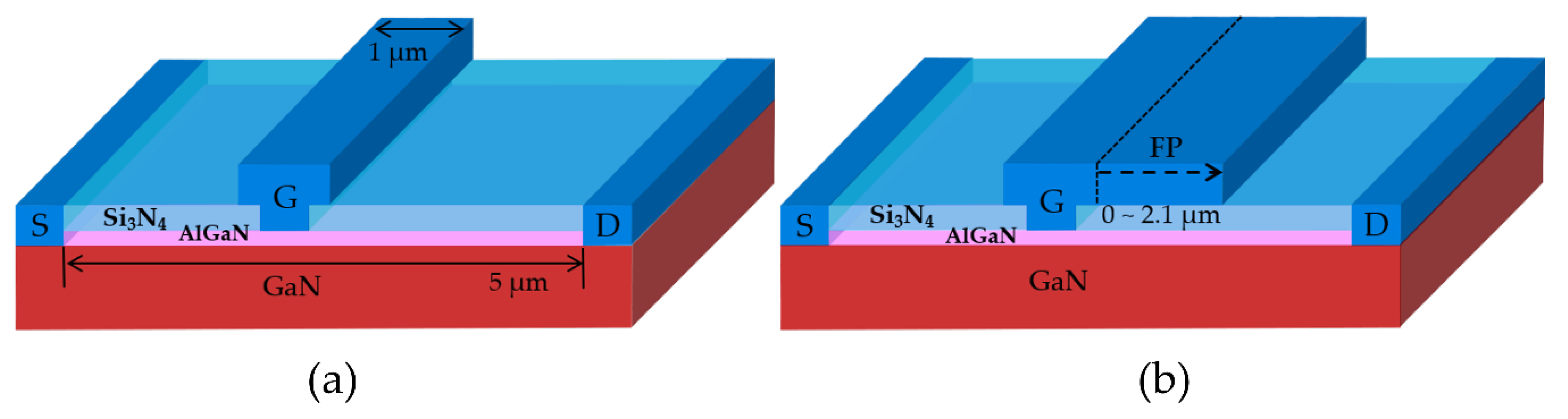
Figure 4a shows the basic structure with the 3D modeling of the device. Generally, many gate FP structures are used to increase the breakdown voltage beyond the stipulated limit for power electronics.
Figure 4b explains the schematics of a drain-side FP device. Except for the drain-side FP length, which was changed from 0 to 2.1 μm to probe into the difference in the breakdown voltage, all the remaining structural variables of the device were fixed.
It is well known that the impact ionization and electron punch-through are two of the most eminent physical mechanisms that breakdown the HEMT devices [
27,
28]. Impact ionization is a direct result of sufficient energy acquisition by an electron in the channel region from a high electric field. The electron punch-through occurs when electrons penetrate through the GaN buffer layer. This leakage current can be prevented by doping the buffer with highly resistive acceptor traps or by employing back barrier in the GaN buffer layer to confine the electrons only in the channel region. This analysis focuses on the breakdown characteristics caused by the impact ionization and electron punch-through effects. To consider both mechanisms, the impact ionization model and the substrate acceptor doping were applied as shown in
Figure 2. In AlGaN/GaN HEMTs, a common approach used to enhance the breakdown voltage is to redistribute the electric fields over the channel by employing an FP structure. The electric fields originate at the corners of the gate electrode. Premature impact ionization results in a soft breakdown in the source-side FP structure [
29], whereas the drain-side FP undergoes a hard breakdown, owing to a delayed impact ionization following the avalanche process. In FP technology, there is a direct dependence of breakdown voltage on the correlation between the carrier density and the electric field [
30,
31]. Therefore, T-shaped gate FP structures are exploited to account for both source-side and drain-side electric fields and, hence, carrier concentrations. The high electric fields beneath both gate corners are uniformly distributed along the channel by the T-shaped gate, which results in high breakdown voltage. Among all gate-head designs, the highest off-state breakdown voltage with low leakage current can be achieved by the T-shaped gate structure.
Figure 5a presents the breakdown voltage characteristics, showing the leakage current for different drain-side FP lengths. To turn off the channel, a pinch-off voltage of −7 V was provided for breakdown voltage measurement via the transient simulation method. Although an increase in FP length reduced the overall off-state drain leakage current, impact ionization-based breakdown characteristics were recorded in the 2-DEG channel layer near the drain-side FP edge. Hence, the drain-side FP edge is a critical factor to be considered for the reduction in the breakdown voltage of the device.
Figure 5b shows the peak breakdown voltages at different FP lengths. The breakdown starting point was the spot where the leakage current was 1 mA/mm according to the development specification of radar systems. A normal T-shaped gate structure, without any extension, has a breakdown voltage of 151 V. The breakdown voltage relates directly to the FP length because of the extension of the gate edge point redistributing the peak electric field in the channel layer and a reduction of the electron punch-through effect. The propounded results also coincided with the experimental results presented by other groups [
32,
33,
34,
35]. The maximum breakdown voltage of 669 V was achieved with the FP length of 0.8 μm. A further increase in the FP length beyond 0.8 μm decreased the breakdown voltage because of an utter increase in the high electric field-driven impact ionization process near the drain-side FP edge. The
and
did not change with the drain-side FP extension.
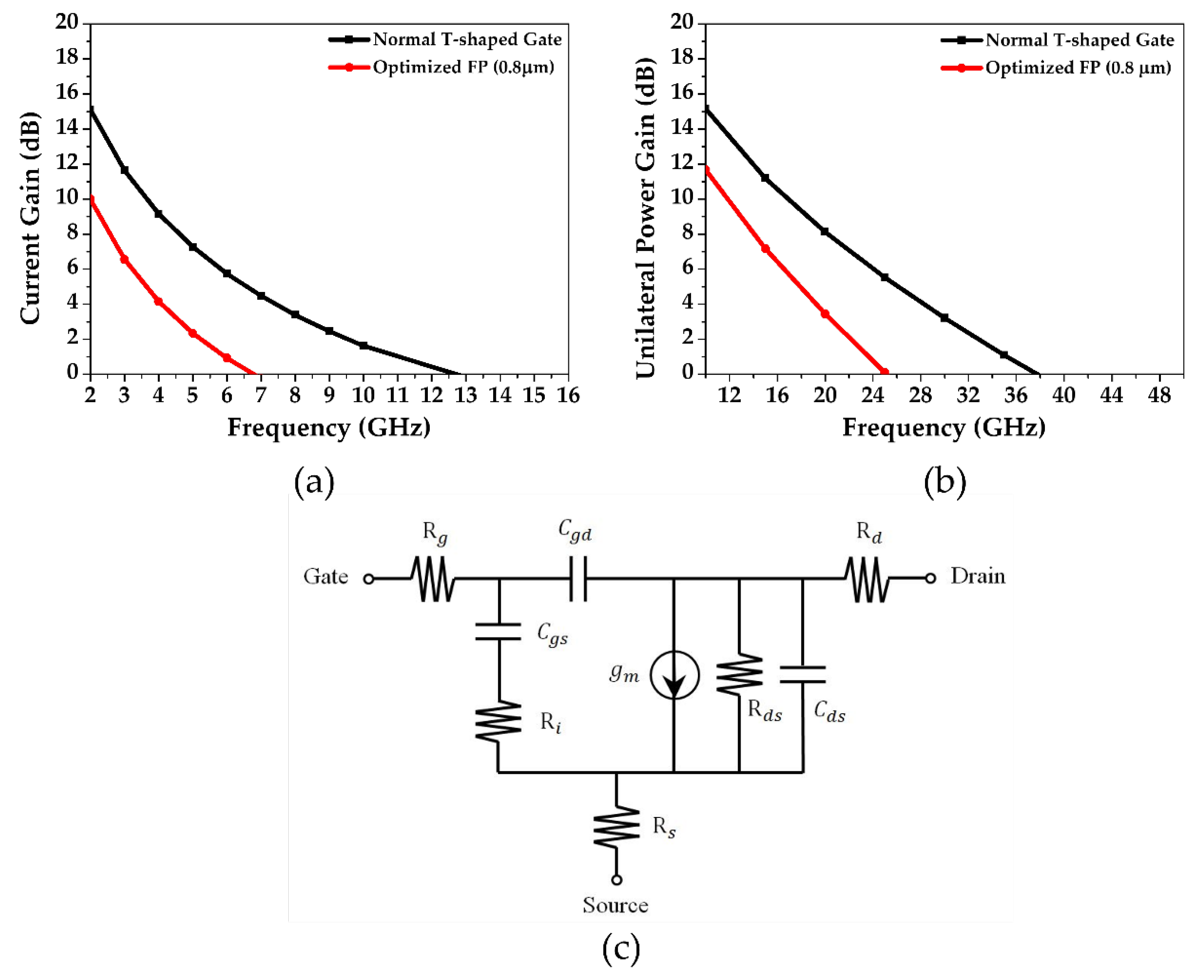
The drain-side FP structure significantly increased the breakdown voltage, but the RF characteristics of the device were deteriorated.
Figure 6a shows the current gain characteristics of the device for fixed DC parameters at V
ds = 12 V and V
gs = −2 V. The optimized 0.8 μm FP structure showed the
of 6.7 GHz, where the value of the normal T-shaped gate structure was 12.7 GHz. It was seen that the response characteristics were reduced to 52.8%. The unilateral gain of the device followed a similar trend, as shown in
Figure 6b. The
of the optimized FP structure and normal T-shaped gate structure were 25 and 37.6 GHz, respectively, which indicates 66.4% degradation. Equations (4) and (5) explain the small signal equivalent circuit [
33,
34,
35,
36,
37],
where
and
dominate the decrease of
and
. Parasitic capacitances need to be reduced for higher
. Source resistance, gate source resistance, and source inductance are designated as
,
, and
, respectively. Gate resistance (
and output conductance (
) are other important components when considering the fabrication process [
35]. Decreasing the denominator components would help to increase the
. The circuitry arrangement is shown in
Figure 6c and contains parasitic resistances and capacitances. Considering the limited importance of the inductive components, they were not considered for device optimization.
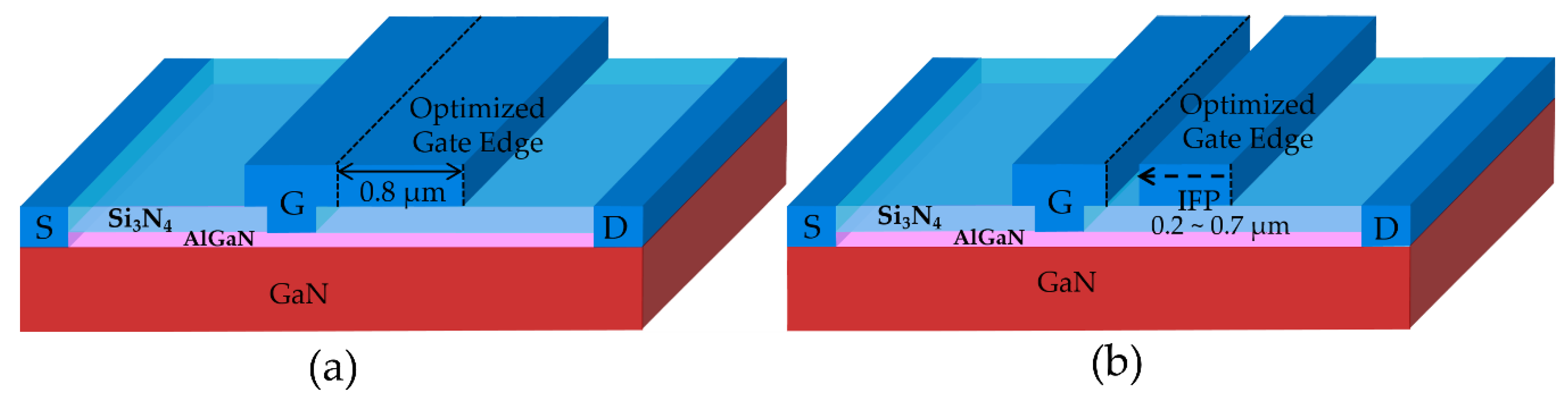
Figure 7a shows the schematic illustration of an optimized 0.8 μm FP structure. There are certain limitations with drain-side FP structures because of their low RF characteristics. The breakdown voltage of the conventional T-shaped gate structure was not high enough, and the RF characteristics were dropped with the optimized FP structure. Hence, the IFP structure was adopted to minimize the capacitance increment, so that it could increase the RF response and minimize the breakdown voltage degradation. The IFP structure was applied on the basis of the operation of an optimized FP structure.
Figure 7b shows the schematic of an IFP structure, stretching from a 0.8 μm optimized gate edge spot towards the gate direction. The length of the IFP structure was increased from 0.2 to 0.7 μm. Hence, six different IFP lengths, i.e., 0.2, 0.3, 0.4, 0.5, 0.6, and 0.7 μm were analyzed. When the IFP had a length of 0.7 μm, a 100 nm gap was deliberately left between the IFP and the T-shaped gate. On the basis of the gate edge of the optimized FP structure, the aggregate length of the IFP and the gap are always set to 0.8 μm. Although the IFP structure and the gate were separated, they were assumed to be connected, so that the same gate bias was provided to both.
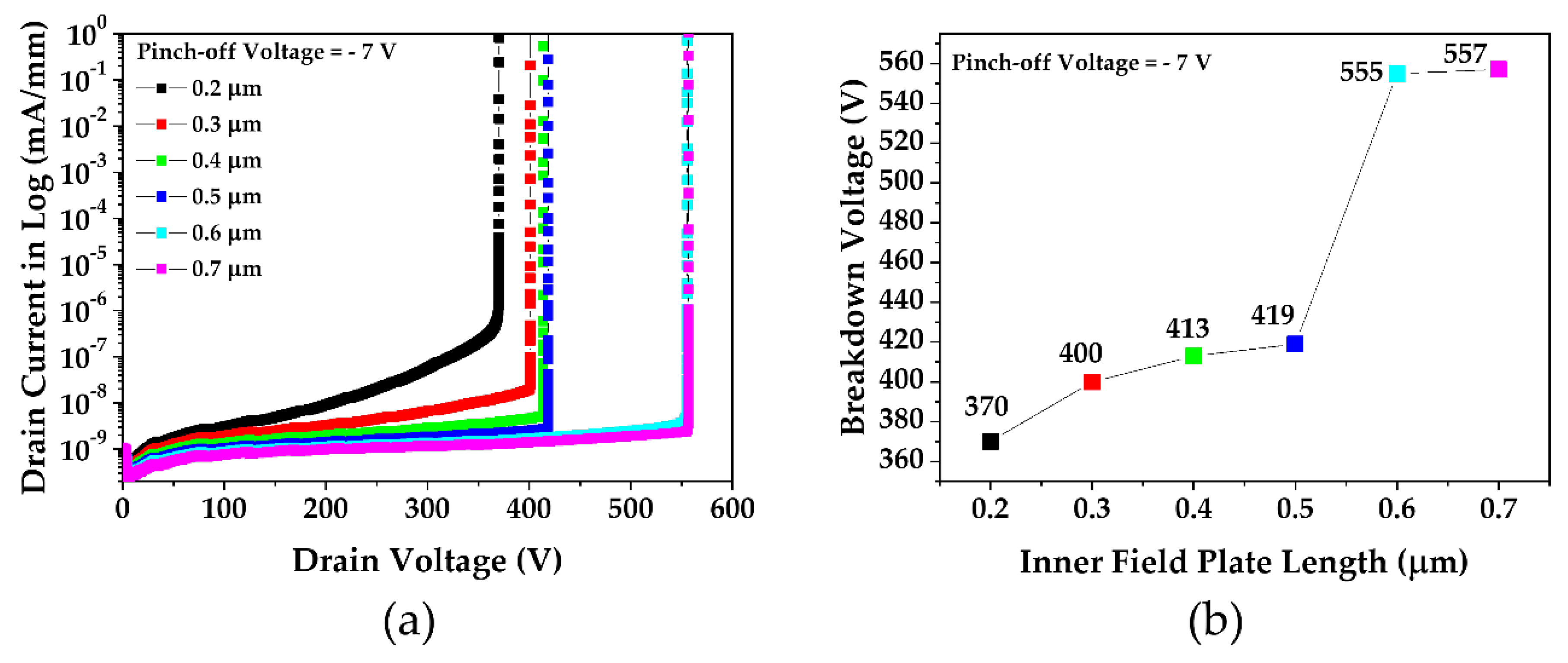
The breakdown voltage of the IFP structure was analyzed accordingly. As shown in
Figure 8a, some degradation was found in the breakdown voltage of the device. The extension of the IFP towards the drain-side gate head edge reduced the drain leakage current in the off-state condition.
Figure 8b indicates the peak values of the breakdown voltage as a function of the IFP length which were 370, 400, 413, 419, 555, and 557 V for IFP lengths of 0.2, 0.3, 0.4, 0.5, 0.6, and 0.7 μm, respectively. The breakdown voltage changed abruptly between 0.5 μm and 0.6 μm. Though there were some decreases, all values were much larger than the values for a normal T-shaped gate structure.
Small signal RF analysis was performed on different IFP lengths for fixed DC parameters at V
ds = 12 V and V
gs = −2 V. The current gain decreased monotonically when the IFP was stretched from 0.2 to 0.6 μm, and started to slightly increase with any further IFP stretching beyond 0.6 μm. The
of 0.2 μm IFP structure was formed near 9.05 GHz, which was 35.1% better than for the connected structure, as shown in
Figure 9a. The unilateral power gain was changed with different IFP lengths because of changes in the device capacitance, as shown in
Figure 9b. At the IFP structure, when the IFP length was 0.3 μm,
was higher than for other IFP lengths. The highest
of 25 GHz was achieved when the IFP was connected to the gate.
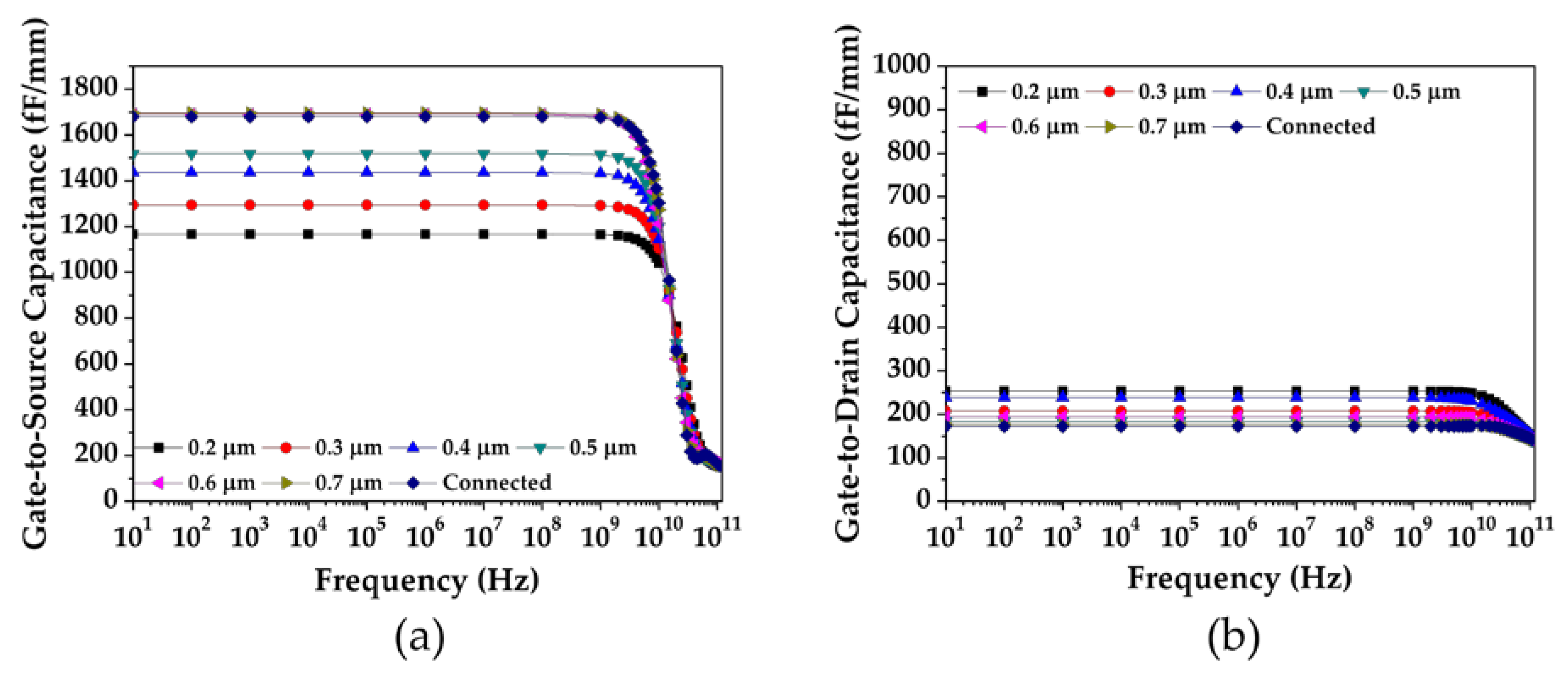
Furthermore, the capacitance was extracted to probe the relationship between frequency and capacitance.
Figure 10 shows the capacitance variations for different IFP structure lengths. The
, which is directly proportional to the IFP length, showed the smallest value for an IFP structure length of 0.2 μm. Finally,
had a saturated value of about 1690 fF/mm. However, compared to
, only a little change in
was observed for various IFP lengths. The changes in the geometrical length of the drain side can affect both
and
[
14,
15]. Although the geometry was changed only in the drain side, the
variation was much larger than the
variation. The drain-side FP not only affected its drain-access capacitance but reflected an influence on the source-access capacitance, and vice versa for the source-side FP. The coexistence of the FP own extrinsic capacitance along with the intrinsic capacitance beneath the gate edges (gate-source and gate-drain) due to the depletion region is cited as the reason for the said phenomenon [
17,
38]. The FPs regulate the depletion layer by a uniform distribution of the electric field beneath both gate edges. The electric field redistribution by FPs along the gate edges results in the suppression and extension of the channel depletion length, hence raising the capacitance [
14]. In the device configuration, as depicted in
Table 1, L
SG was shorter than L
GD. Therefore, initially,
was larger and more influenced by the changes in the IFP structure.
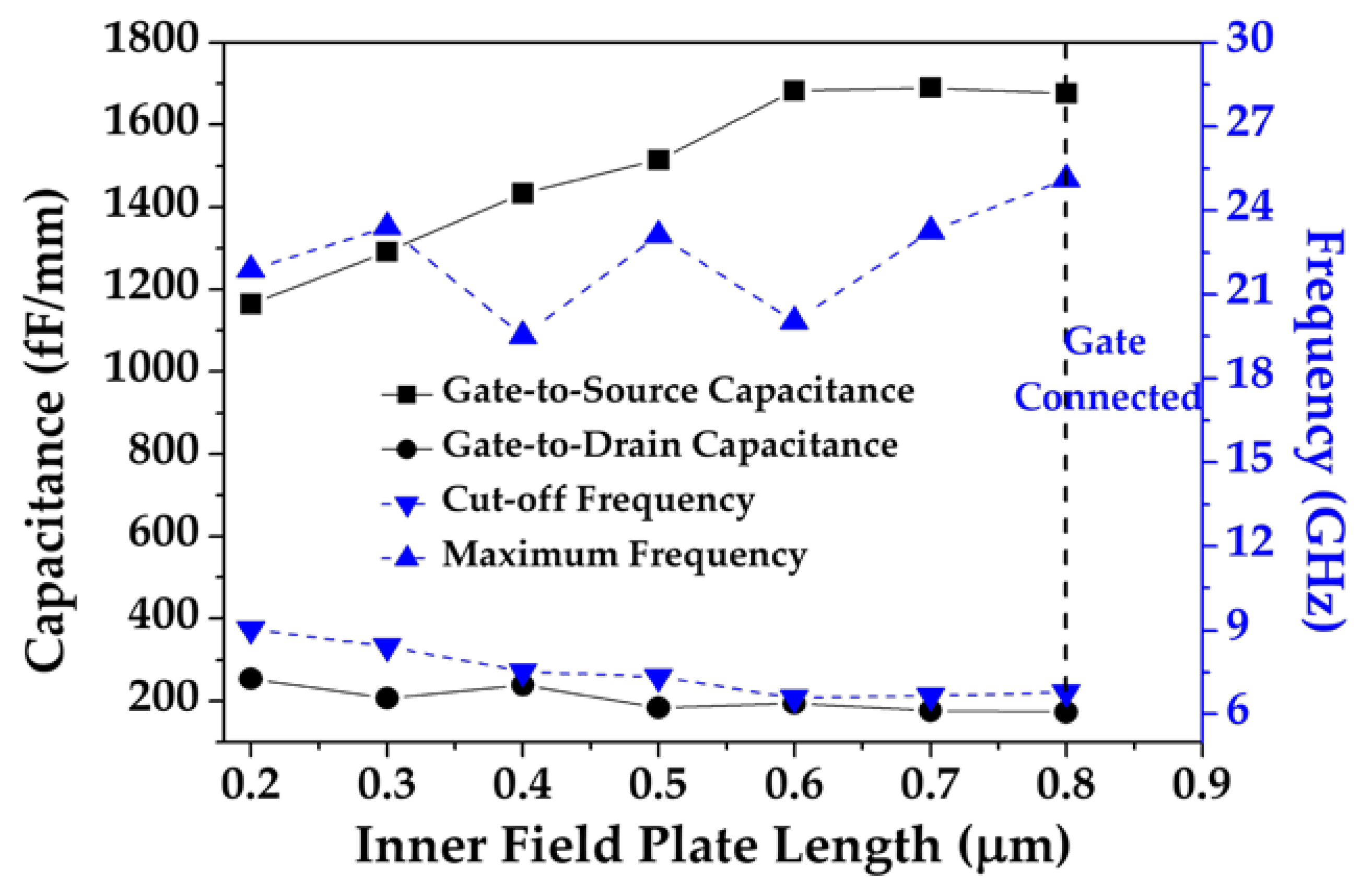
Figure 11 summarizes the frequency and capacitance variations as a function of IFP lengths in order to verify the dependence of the frequency upon the capacitances. The drain-side IFP increased
to moderate
, as shown in Equation (4). A dominated sum of
and
is responsible for the degradation in
. To alleviate this factor, the IFP length should be reduced. However, this also results in an increase in
that affects the
, as shown in Equation (5). Consequently, to achieve both high
and
, the gate-head optimization is inevitably required. Hence, 0.2–0.3 μm IFP structures were found to be the final optimum structures and are thus highly recommended for a comprehensive usage of the HEMT device.
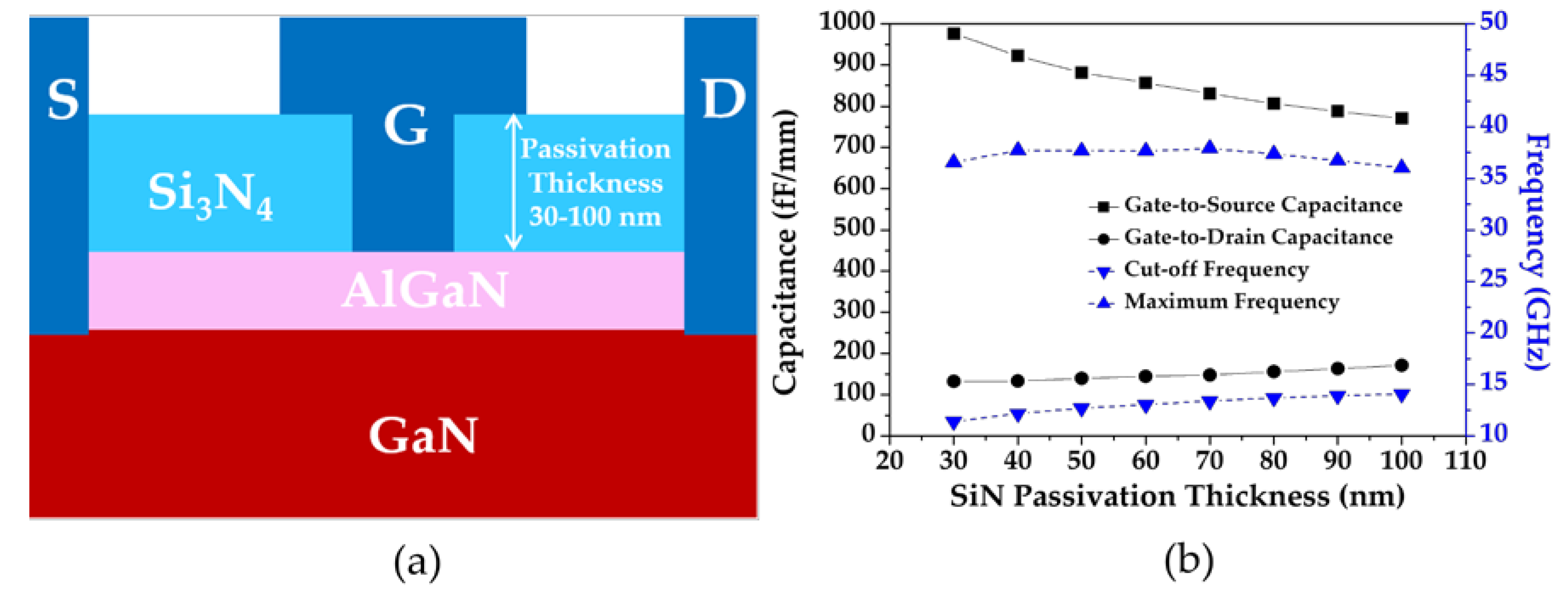
A Si
3N
4 layer was used below the T-shaped gate because it is a good surface passivation film which provides a high dielectric constant and breakdown strength and minimizes the current collapse [
2]. The frequency variation from differences in Si
3N
4 passivation thickness was also analyzed.
Figure 12a shows that the passivation thickness changed from 30 to 100 nm, with consequential cut-off and maximum frequency effects, as shown in
Figure 12b. The value of
decreased with an increase in the Si
3N
4 passivation layer thickness, which consequently increased the
. However,
showed only a little increase with an increase in the Si
3N
4 layer thickness. The highest
and
were 14 and 37.8 GHz with Si
3N
4 layer thicknesses of 100 and 70 nm, respectively. Hence, because of the dependence of device’s RF parameters on the passivation layer thickness, the Si
3N
4 layer thickness was also regarded as an important factor for power applications of the HEMT device.


