Energy Management Integrated Circuit for Multi-Source Energy Harvesters in WBAN Applications
by
Sung-Eun Kim
*, 
Taewook Kang
,
Kwang-Il Oh
,
Mi Jeong Park
,
Hyung-Il Park
,
In Gi Lim
and
Jae-Jin Lee
SoC Design and Research Group, Intelligent SoC Research Department, Electronics and Telecommunications Research Institute, Daejeon 34129, Korea
*
Author to whom correspondence should be addressed.
Appl. Sci. 2018, 8(8), 1262; https://doi.org/10.3390/app8081262
Submission received: 13 July 2018
/
Revised: 25 July 2018
/
Accepted: 27 July 2018
/
Published: 31 July 2018
(This article belongs to the Special Issue Body Area Networks)
Abstract
:This paper presents an energy management integrated circuit for multiple energy harvesters in wireless body area network applications. The electrical power acquired from a single energy harvester around a human body is limited to micro watts, which is insufficient to drive a wearable electronic device. To increase this small amount, the energy from a number of harvesters has to be combined. By combining the energy from multiple distributed harvesters, each one producing negligible energy, significant energy for wearable devices can be obtained. In designing an energy management circuit for a wearable device, there are two issues to be resolved. The first is related to the power consumption of the circuit, and the second issue is related to the methods needed to manage the wide range of power that occurs as the energy input changes during harvesting. In this paper, an energy management circuit that resolves the two issues above is described. The circuit was integrated using 0.13 µm Taiwan Semiconductor Manufacturing Company complementary metal-oxide-semiconductor technology. The energy management circuit is designed to combine up to three sources of harvested energy with more than 90% operating efficiency over the entire power range of the energy harvested.
1. Introduction
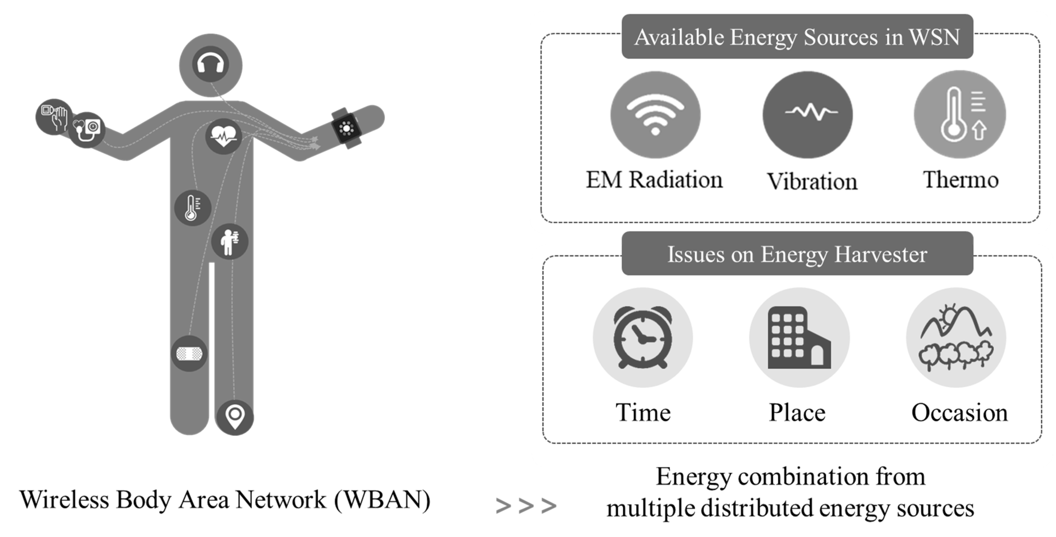
Wireless sensor networks (WSNs) are being developed for personal applications of wireless body area networks (WBANs). With the development of integration technologies, the size of a wireless sensor node has become so small that it can be used on human bodies in the form of wearable devices. However, there are still challenging issues in realizing wearable devices. One of the most important issues is battery maintenance. Periodic battery charging and replacement in wearable devices is a task quite cumbersome to users. To overcome this issue, the designs for wearable devices are beginning to adopt some of the renewable energy sources that have been investigated in recent decades. Renewable electrical energy can be obtained from light [1,2], vibration [3,4], heat [5], and electromagnetic radiation [6,7]. Energy harvesting technology that extracts electrical energy from those renewable energy sources is expected to offer a solution to the energy limitations of current wearable devices.
With wearable devices on a human body (as shown in Figure 1), the available energy sources are limited to body movement, body temperature, and electromagnetic energy associated with the human body. The magnitude of power that can be acquired from these energy sources is limited to micro watts [8], and this is insufficient to drive wearable electronic devices. A micro watt of harvested power is generally regarded as useless in electronic devices, and conventional energy management research has been focused on extracting more power from energy harvesters by matching impedance. Unfortunately, with micro watt power harvesters, the method of extracting more power with complex algorithms is not helpful to increase the power output. Rather, the power required to extract output power may be greater than the potential for increase in the output power. Therefore, in WBAN applications, the algorithm approach for extracting more power is not appropriate. Instead of extracting more power from an individual energy harvester, combining energy from multi-source energy harvesters is more worthwhile. The most common conventional structure for combining energy is the diode-based power OR-ing method [9,10,11], which is also the simplest way to combine energy from multiple sources. However, this approach has one drawback: unwanted power consumption caused by a forward voltage drop on the diode. Recently, to avoid waste of power in the diode based OR-ing circuit, an active switch can be used in place of a diode. An active switch can resolve the problem of the forward voltage drop, although it introduces a new issue of power consumption.
In designing energy combining circuits for WBAN applications [12,13,14,15], power consumption is one of the most important issues. As mentioned, the power from each energy harvester is limited to micro watts, and the energy combining circuit has to consume less power than the power harvested. If the combining circuit consumes more power than that harvested, no energy can be supplied to the wearable devices. To reduce power consumption, the energy combining circuit should be simple in structure and guided by an algorithm. In energy harvesting circuits, there is one more issue to be considered. In addition to power consumption issue, the circuit also has to manage a wide range of harvested-energy levels. The amount of harvested energy varies according to the environmental conditions under which each specific harvesting transducer operates [16]. Therefore, the energy management circuit should handle a wide range of harvest-energy levels.
In this paper, an energy management circuit is presented that combines multiple input energies, and which distributes multiple input energies to dual output loads with low power consumption. By combining input energy from multiple sources, significant energy can be acquired from multiple sources of individually negligible energies. Then, by distributing the output loads, the excess energy (the amount that exceeds that consumed in the load stage) can be utilized to charge a rechargeable battery. These two main functions were implemented in an energy management circuit, and it consumed just 1.5 µW with 1.2 Vdd. One of the major contributions of this work is that it shows the potential for utilizing a variety of low-power energy harvesters. In the future, the energy sources that were thought to be useless previously could be utilized in electronic devices, and everlasting wireless sensor nodes without the need for battery charging or replacement might be possible.
To present the new energy management circuit, this paper is organized as follows. First, the conventional method used to combine energy from multi-source energy harvesters is analyzed. Then, the newly proposed architecture, circuit design, and novel algorithm for managing energy from multi-source energy harvesters with dual loads are described. Finally, experimental results are presented.
2. Conventional Structure
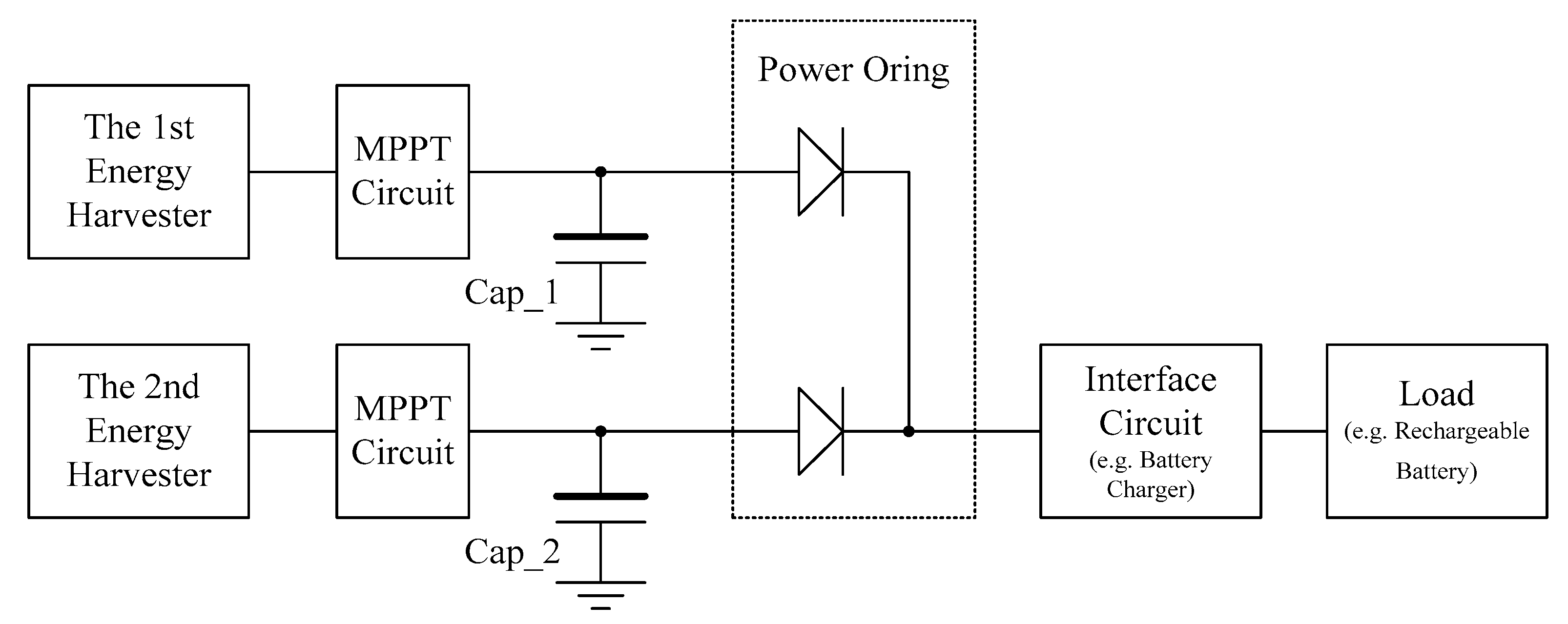
The conventional architecture of a combining circuit for a multi-source energy harvester (EH) is depicted in Figure 2. Although Figure 2 shows just two energy harvesters, the number of energy harvesters could be expanded. Each energy harvester converts a certain kind of ambient energy to electrical energy. The maximum power point tracking (MPPT) circuit extracts maximum power from each energy harvester by adapting the impedance conditions. The conventional method by which the energy extracted by each harvester is combined is called the “power OR-ing method” [9,10,11], and this is the simplest method to combine energy from multiple sources. The interface circuit (such as a dc-dc converter) converts the output voltage to a level appropriate for the load devices.
If the energy from each harvester is sufficient, the conventional architecture may be optimal. The unanticipated waste of power that occurs while combining the energy streams can be ignored, and does not affect the result of efficiency gained by combining the energy stream. However, for low power applications such as WBANs, the architecture must be simplified. For this use, the MPPT circuit is not appropriate. It includes a complex algorithm to track and compare the magnitude of harvested power. This may consume more power than is possible to provide in a WBAN. Therefore, eliminating the MPPT circuit may improve the power supplied to a load. In this work, because the application involved micro watt power levels, the MPPT circuit was not taken into account.
Next, the OR-ing circuit also needs to be improved. The diode-based power OR-ing circuit has one drawback; there is unwanted power consumption caused by the forward voltage drop on the diode. The forward voltage drop can be minimized with a low forward voltage diode such as Schottky diodes. However, power waste due to the forward voltage drop when using the diode based power OR-ing method is inevitable. To avoid such power waste, a metal-oxide-semiconductor field-effect transistor (MOSFET) switch can be used in place of the diode. The MOSFET based power OR-ing circuit also requires power consumption to drive the circuit. However, as the integration process proceeds, the power consumption of a circuit is reduced continuously.
Aside from the unwanted energy loss in a conventional OR-ing stage, both diode based power OR-ing circuits and MOSFET based power OR-ing circuits have one more common drawback in common. When the one energy harvester generates greater energy than the other harvesters, the power OR-ing method causes the energy streams from the other harvesters to be excluded. Thus, low energy harvesters have no chance to contribute their energy to a load device. For example, when two harvesters are photovoltaics (PV) and piezoelectric (PZ) respectively, on a sunny day, the PV transducer generates much more energy than the PZ transducer does. The voltage of energy stored in the PV capacitor is higher than the voltage of the energy stored in PZ capacitor, and only the energy of PV harvester can be transferred to the load through the interface circuit. Until the voltage of the energy stored in the PV capacitor drops below the voltage of the energy stored in the PZ capacitor, the energy harvested in the PZ transducer has no chance to be connected to a load. The energy in the PZ just waits to be connected and the harvested energy may disappear due to the leakage characteristics of its temporary storage. In low power applications like WBANs, all the harvested energy should be saved carefully. It is not desirable to entirely exclude any of the harvesters in any case. To prevent the exclusion of a specific harvester, the magnitude of the energy in all harvesters should be monitored periodically and the energy from each harvester should be moved to storage.
Moreover, if the harvester generates more energy than the energy consumed at the load, the voltage of the temporary storage capacitor keeps increasing. Then the excess harvested energy does not contribute to the power consumption of the load and the increasing voltage of the temporary storage may induce damage to the circuit. Therefore, when the harvester generates more energy than is consumed at the load, another way of utilizing the extra energy should be considered.
3. Energy Management Integrated Circuit (EMIC) Structure
3.1. Energy Management with a Single Harvester
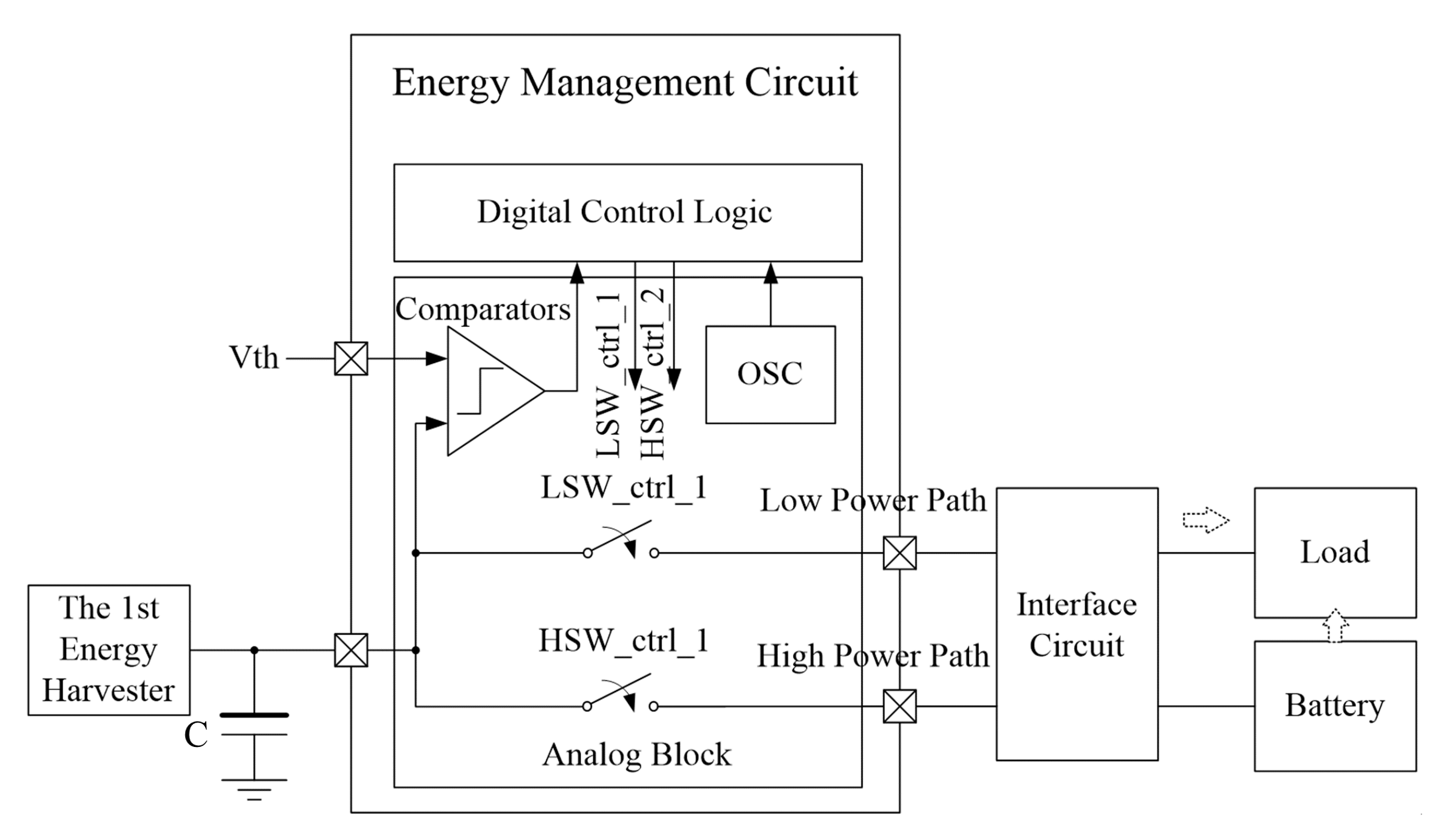
The proposed architecture for the energy management circuit is shown in Figure 3. This architecture is simplified to the case of single energy harvester to help with comprehension of the operating algorithm of the proposed energy management circuit.
Because the amount of energy harvested changes according to environmental conditions, the energy management circuit adopts a dual load scheme to deal with a wide range of energy levels. A dual load scheme has two output paths: a low-power path and a high-power path. According to the magnitude of the energy harvested, the energy can be supplied through either the low-power path or high-power path. As shown in Figure 3, the architecture provides a load in the low-power path, and a storage element such as a rechargeable battery in the high-power path. Normally, harvested energy is supplied to a load directly. If the energy in a harvester exceeds the energy consumed by a load, the extra energy is stored in a storage element. By storing the extra power in a storage element, the excess power can be utilized in the load later.
With this architecture, the capacitance provided is an important factor and determines the operating clock frequency. This affects the power consumption of the circuit. Because a circuit with high operating clock frequency consumes more power, the capacitance should be considered carefully. The equation for sizing capacitance is derived below.
In Equation (1), Q is the quantity of charge, C is the size of capacitance, and V is the voltage of the capacitor. When Q is differentiated with time, the current can be described as the product of the capacitance size and the voltage change, as shown in Equation (2). The current into the capacitor is proportional to the speed of the voltage change in the capacitor. When current is harvested in the input stage, the voltage of the capacitor rises. The speed of voltage change in the capacitor is determined by the capacitance. If the voltage in the capacitor changes rapidly, the integrated circuit (IC) should check the voltage more frequently. Therefore, the relation between capacitance and operating frequency of the IC is very close. Equation (2) also shows the relation between capacitance and the current consumed at the load stage. When power is consumed at the load stage, the voltage of the capacitor starts to fall. To prevent the voltage of the capacitor from falling below the threshold voltage, the size of the capacitor and the operating frequency of the IC should be controlled appropriately. To slow the operating clock frequency, large capacitance is preferred. The operation starts with the energy harvested from an energy source. When the energy is harvested, it is stored in a temporary storage capacitor, C, which rises the voltage of C. The voltage of C is periodically checked by internal comparators whether the voltage of C is higher than threshold voltage, Vth, or not. If the voltage of C is higher than Vth, the switch in the low-power path turns on, and the stored energy in C is supplied to a load through the low-power path. If the harvested power is less than the power consumed by the load, the voltage of C will decrease, and the switch on the low-power path turns off. If not, the voltage of C keeps increasing. Then, the switch on the low-power path turns off, and the switch on the high-power path turns on. The energy stored energy in C is connected to the battery through the high-power path instead of to the load in the low-power path. Thus, when the harvested power exceeds the load power, the harvester power is used to charge a battery. By adopting dual output paths, a wide range of input energy can be handled.
3.2. Energy Management with Multi-Source Harvesters
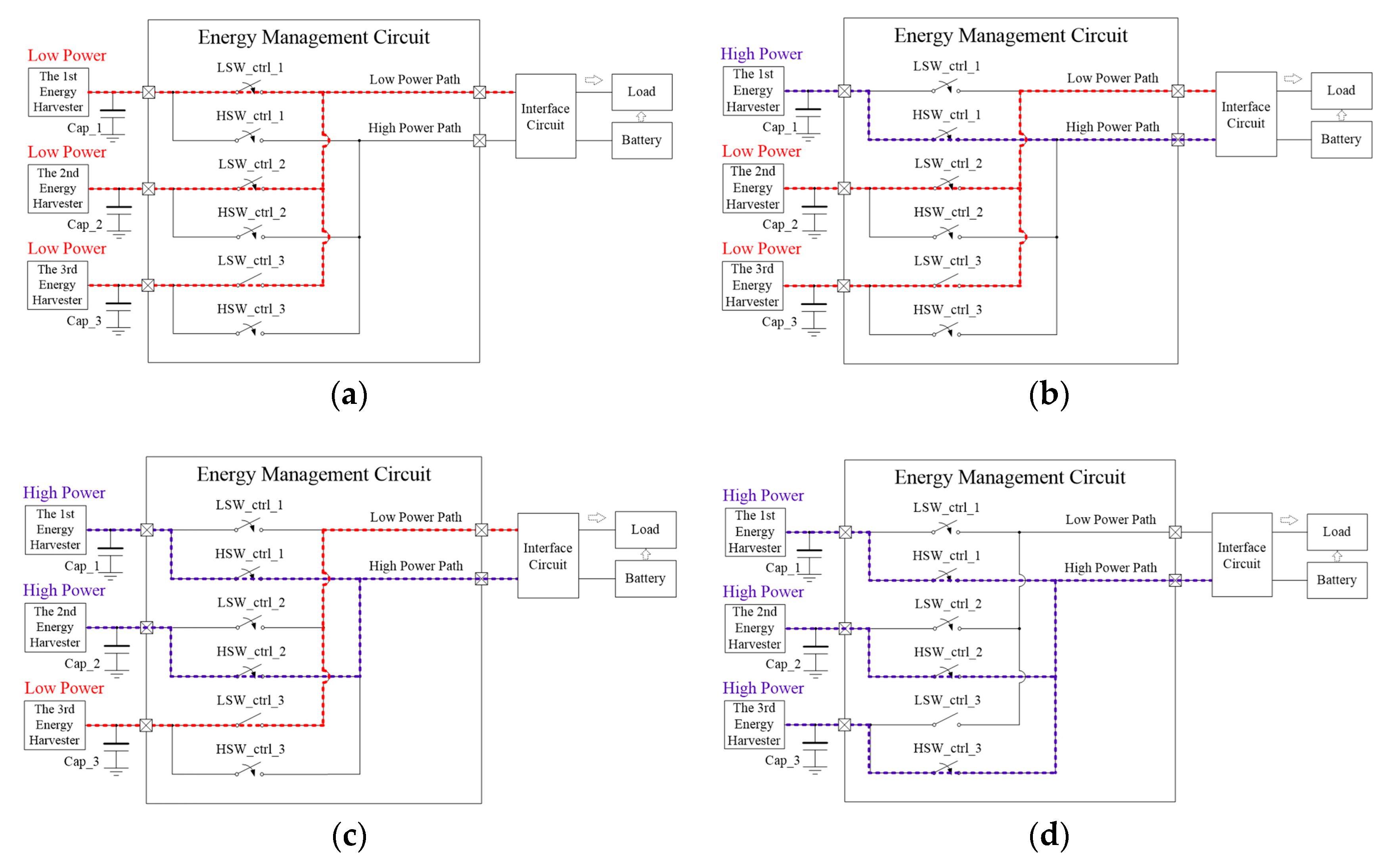
The proposed energy management circuit has three input ports and two output ports. Up to three energy harvesters can be attached to the circuit, and two loads can be supported. According to the condition of the harvested energy, sometimes the energy streams from multiple harvesters are combined to one output port by sharing time, and sometimes they are distributed to two output ports. There are four different cases for the conditions under which the energy is harvested.
The four different cases with input conditions are described in Figure 4. For the case illustrated in Figure 4a, all three energy harvesters generate low power. The three harvesters are connected to the low-power path, and supply energy to a load by sharing time. The difference between this and combining energy using the power OR-ing method is that with the proposed method, all three harvesters are monitored and each is given a chance to be connected to the low-power path. This prevents the energy already harvested from dissipating while in temporary storage.
For the case illustrated in Figure 4b, the power of the first harvester is high, while the power of the other harvesters remains low. As in the first case, the energy of the first harvester is checked, and then connected to a low-power path. If the power of the first energy harvester is higher than the power consumed by the load, the voltage in Cap_1 remains higher than the threshold voltage, Vth. Then, when the next check is done, the first harvester is switched to a high-power path. The first harvester starts to supply energy to a battery, and the voltage in Cap_1 starts to decrease. At the time of the next check, the first harvester is again connected to a low-power path. The other harvesters still supply energy to the low-power path sequentially as in the first case.
In the case illustrated in Figure 4c, the second harvester is producing high energy, and only the third harvester is generating low power. The first and second harvesters supply energy to a load and the battery in sequence, while the third harvester supplies energy to a load. In the last case, Figure 4d, all three harvesters produce high energy and all three supply energy to a load and to a battery at the same time. The battery is charged using the energy from all three harvesters. When no harvest-energy stream is passing to the load, the energy in the charged battery can be utilized by the load through a diode or an additional switch.
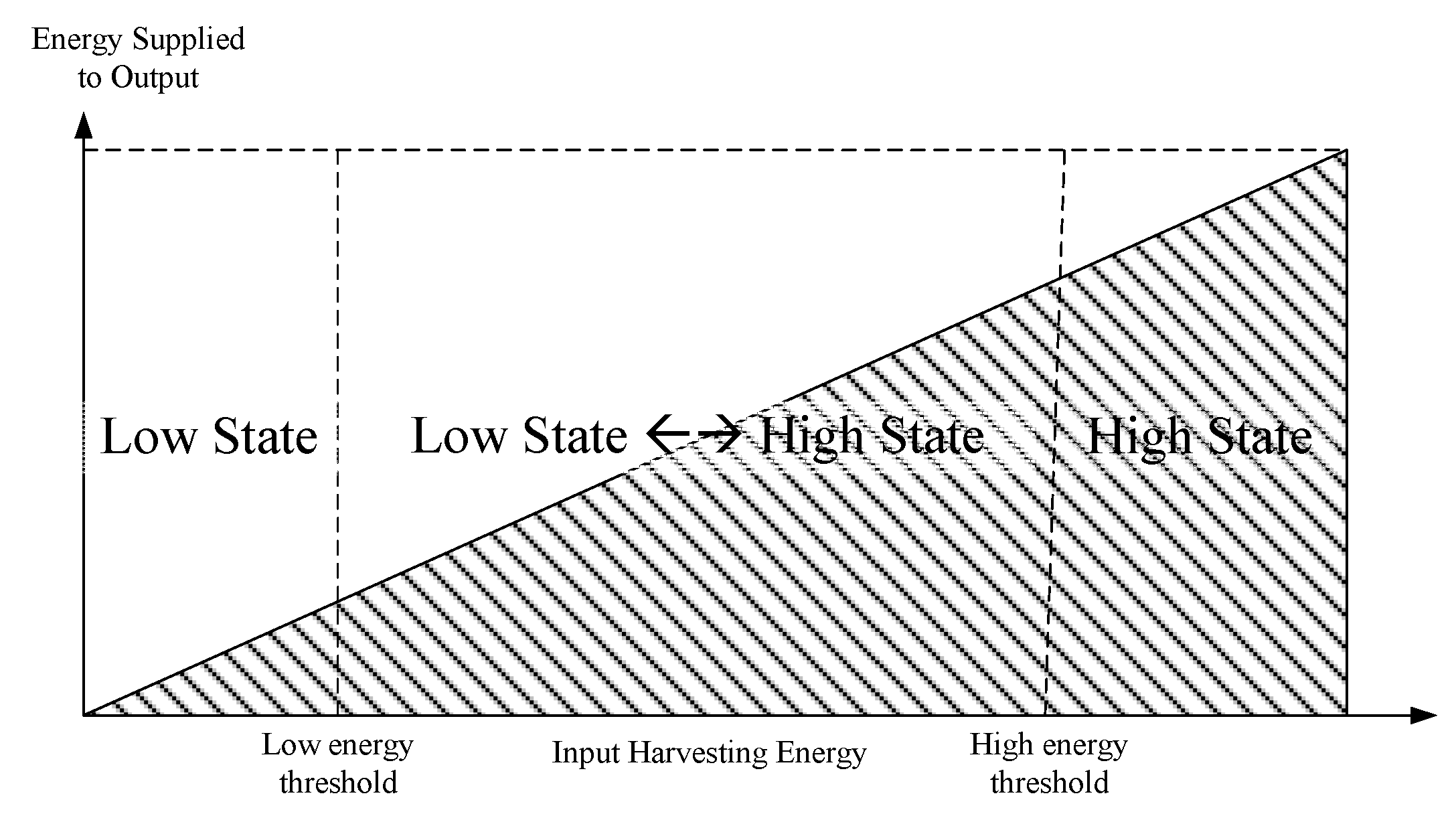
The energy output path for a harvester is selected according to the amount of energy harvested. There are three output-path states as classified by the energy threshold levels described in Figure 5. The low energy threshold is determined by the energy consumed in the low-power path, and the high energy threshold is determined by the energy consumed in the high-power path. When the amount of energy harvested is lower than the low energy threshold, the harvester always supplies energy to a low-power path. When the amount of harvested energy is between the low energy threshold and high energy threshold, the harvested energy is supplied to low and high-power path alternately within a given time interval. When the amount of harvester energy is higher than the high energy threshold, a harvester provides energy only to the high-power output path.
4. Circuit Block Designs
The energy management circuit has an analog part and a digital part. The role of the analog part is to generate clock signals, monitor the state of the harvested energy, and to choose a path from the input port to the output port. The digital part makes sure the path combinations are energy efficient.
4.1. Analog Blocks: Path Switches, Comparators, and Oscillator
One analog blocks is composed of path switches, comparators, and an oscillator. The path switches are managed using digital control logic to determine the output paths used to supply the input energy. The two output paths (low-power path and high-power path) are shown in Figure 6a. In this system, the input ports are constrained to three choices. The number of input ports can be expanded according to the needs of an application.
When designing path switches, the resistance of a switch is a major factor to be considered. Switches with high on-resistance can lose relatively large amounts of power during energy transmission. The equation for dissipated power in a path switch is
In Equation (3), P is dissipated power in a path switch, I is the current that flows through the path switch, and R is the on-resistance of the path switch. When current flows through a switch, the power dissipation in the switch is determined by the magnitude of current and the resistance of the switch. This is the reason why the on-resistance of the path switch is very important. If the width of the switch is too small, on-resistance may increase. This may cause too much power dissipation when current flows through the path switch. If the width of a switch is too large, on-resistance may decrease. However, it occupies a large area, and in the off-state, leakage current may also increase. In this case, by using the body bias technique, off-resistance may be controlled. If a current of 10 µA flows through a switch with 1 Ω resistance, 10 µW of power is wasted through the path switch. For low-power applications, 10 µW is not negligible. Ideally, a path switches with no on-resistance, no distortion, and zero time delay is desired. However, it is hard to implement these in real process technology. To minimize the limitations of real process technology, the path switches were designed with bilateral CMOS devices. The on-resistance of both NMOS and PMOS devices changes with the channel voltage. This nonlinear resistance can cause errors in accuracy as well as distortion. By using the bilateral CMOS switch, on-resistance is minimized, and linearity is also improved. The target application of this paper is for WBANs, and the harvest power is limited to micro watt scale. Because an excessively low on-resistance requires a large implementation area, the switch size should be optimized for micro watt scale to achieve efficiency better than 90%.
A comparator detects the magnitude of the harvested energy stored in the temporary storage, Cap_n. The comparator design is shown in Figure 6b. The inputs to comparators are placed on the gates of transistors to show high impedance on the sensed nodes. The role of the comparators is to inform the state of the stored energy in input capacitors to a digital control logic. When the stored energy is higher than the energy threshold, the output of the comparator reaches a high state, and the digital control logic turns on the path switch. After providing the stored energy to the output, the voltage of the input capacitor starts to decrease.
When designing the comparators, operating speed is not an important issue because it detects the voltage of a capacitor. The capacitor stores energy temporarily, and the change of voltage in the capacitor is not rapid. Rather than operating speed, power consumption is a more important issue. To reduce the power consumption in comparators, digital control logic guides the operation of comparators. If no operation is required, the bias currents in the comparators are blocked by an enabling signal from the digital control logic. By adapting enabling techniques, the power can be reduced by as much as 80%. Furthermore, in this system, there is no need for comparator hysteresis. The path switch is controlled by the digital control logic, and the comparators only inform about the amount of stored energy. The digital logic determines the path to be connected at the next clock time. As checking time for the status of the stored energy is not synchronized with the turn on-time for a path switch, the changes in the state of the stored energy after checking the state does not affect the switch operation. When the digital logic sends a switch control signal, the comparator is disabled. Therefore, the transition of the switch between on and off has no effect on the operation of the comparator. Without the need for hysteresis, the comparator becomes simple, and easy to implement.
The oscillator provides clock signals to the digital control logic. The schematic of the oscillator in Figure 6c shows a fully differential relaxation type. Each side of the oscillator is composed of three stage inverters in series. When the voltage of the charging capacitor with a constant current reaches Vref, the comparator shifts the output of the differential amplifier to ground. The grounded output of the differential amplifier discharges the charging capacitor. The repeated charging and discharging in the charging capacitor induces oscillation. The adopted symmetric differential structure increases the overall oscillator loop, reduces the sensitivity to power supply variations and allows seamless oscillation.
4.2. Algorithm for the Control Method
A digital control block generates an enabling signal for the comparators, and a control signal for the path switches based on the output of the comparators. The initial signal enables operation of the comparators, and they are only enabled when there is need to monitor the state of the harvested energy. Periodically enabled comparators detect the amount of energy harvested and inform the state to the digital control block. Based on the state of the harvested energy, the digital control block generates control signals whether to turn on the switch or not. The turn on signal ensures the harvested power is provided to a load.
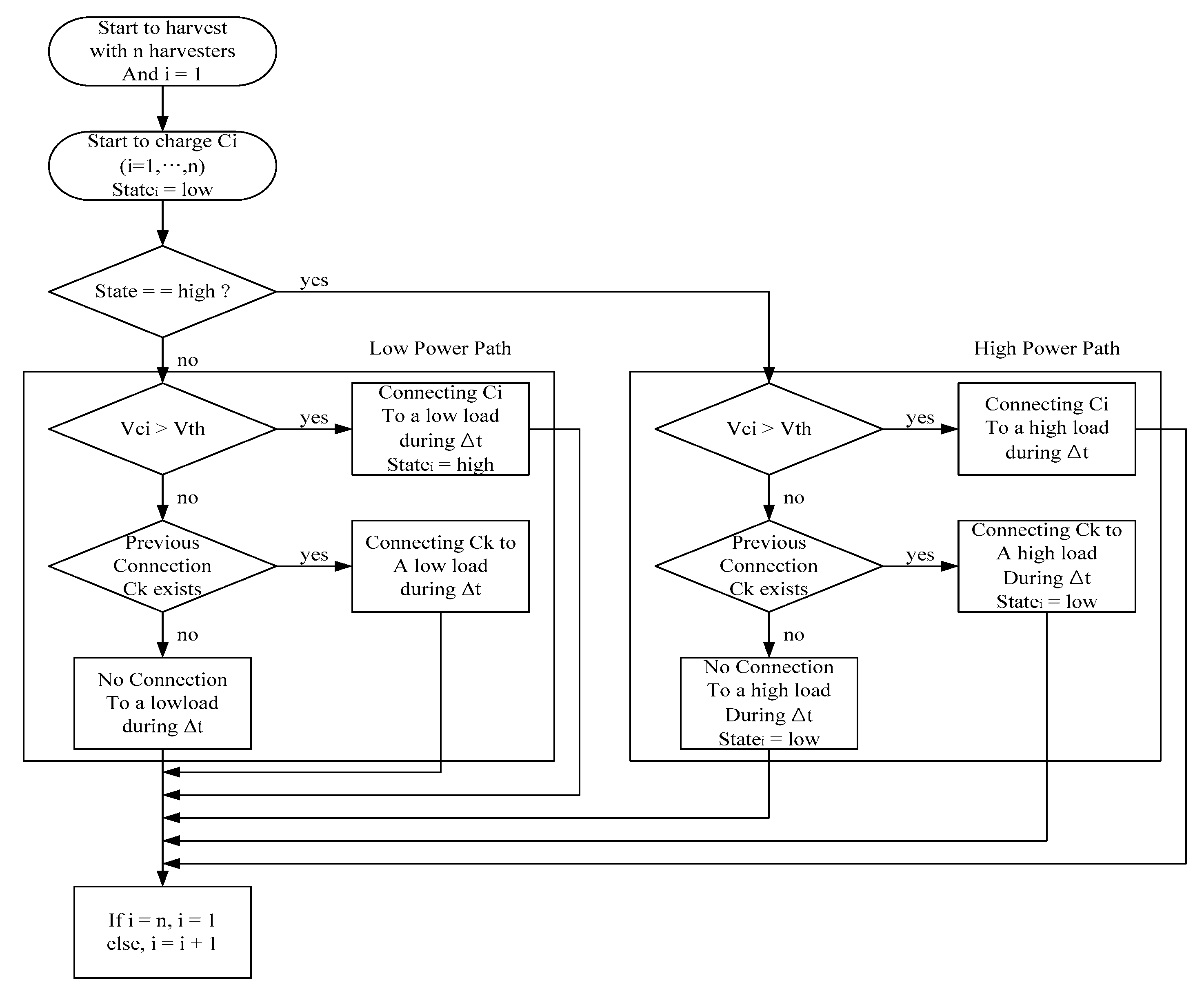
Figure 7 shows a flowchart for the process of the proposed algorithm of the digital control block. When different magnitude of energy is harvested in multiple and multi-type energy harvesters at the same time, the harvested energy should be supplied to a load effectively. To achieve this goal, a novel power managing algorithm is necessary. When n multi-source energy harvesters start to harvest, i is initialized to ‘1’. Here, i is defined as one value among 1, 2, …, n. The harvested energy starts to charge the temporary storage capacitor, Ci. The statei of the ith energy harvester is initialized to a low state. According to the statei, the load to which the harvested energy will be supplied is determined. With low statei, the sequence of low-power path proceeds, and with high statei, the sequence of high-power path proceeds. The algorithms for the low-power -and high-power paths are completely separate, and do not share connecting time. Therefore, in combining energy from multi-source harvesters, the harvesters on the low-power path share time among themselves, and the harvesters on the high-power path allocate time to themselves in parallel with the harvesters in the low-power path.
In the low-power path process, if the voltage of Ci is higher than the threshold voltage, Vth, the energy stored in Ci is connected to a low load during Δt. Then the voltage of Ci begins to decrease, and at the same time, the other storage capacitors except Ci continue being charged from each energy harvester. After Δt, i is changed to i + 1, and the voltage of Ci + 1 is checked. If the voltage of Ci + 1 is lower than the threshold voltage, Ci maintains the connection with a low load. After connecting Ci to a low load, the statei changes to high state. At the next stage, Ci proceeds the high-power path sequence. If i is equal to n, i is initialized to 1, and the process returns to checking state process.
In the high-power path process with a high state, the voltage of Ci is monitored. When the voltage of Ci is higher than the threshold voltage, Vth, the energy stored in Ci is connected to a high load during Δt. After Δt, i is changed to i + 1, and the voltage of Ci + 1 in high state is checked. If the voltage of Ci + 1 is lower than the threshold voltage, Ci maintains the connection with a high load. If the voltage of Ci begins to decrease, the connection Ci with a high load is disconnected, and the state of Ci is changed to low state. If not, the state of Ci is maintained in a high state. The other process is the same as with the low-power path process.
By adopting this novel algorithm, all of the attached energy harvesters have the same chance to supply energy to a load, and the harvested energy is distributed to a load efficiently. According to the magnitude of harvested energy in each harvester, an optimal load is selected to prevent the harvested energy from being wasted. This process is compatible with a wide range of input energy.
4.3. Design of the Digital Control Logic
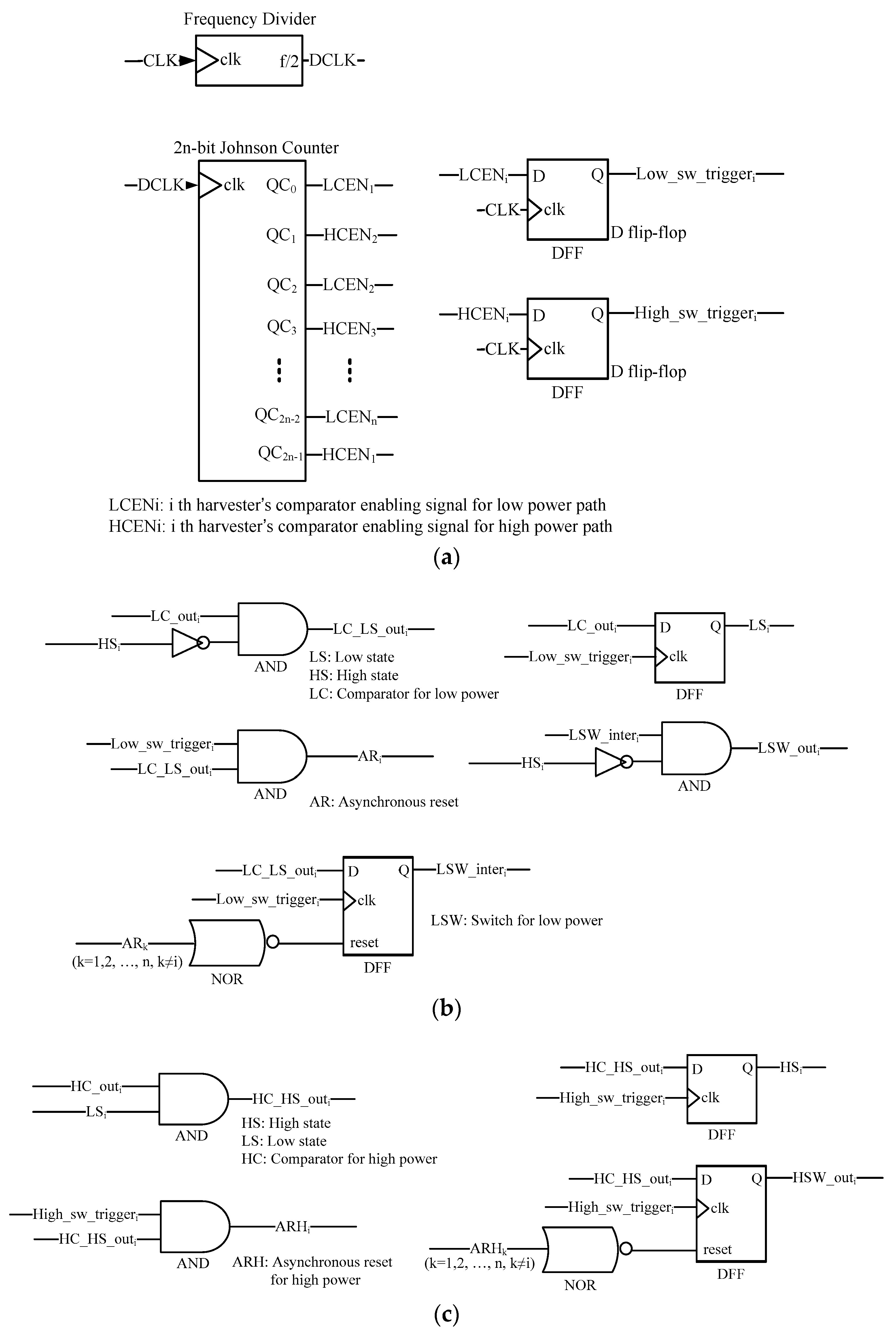
The digital control logic is designed with simple logic blocks as shown in Figure 8. A comparator enabling signal is generated in a 2n-bit Johnson counter as shown in Figure 8a. The clock signal generated from internal oscillator is divided by a frequency divider, and the Johnson counter uses the divided clock as a digital clock. To generate control signal of low-power path switch and high-power path switch for n energy harvesters, a 2n-bit counter is required. After enabling the comparator, the path switch is triggered with D flip-flop. The check period, Δt, is defined as twice as the period of the rising edge in the output signal.
Control signals for low-power path switches can be generated by the block in Figure 8b. With n energy harvesters, n low-power path switches are required. The state of the ith input energy is defined with LSi and HSi state signals. When input energy is low, LSi turns to ‘0’, and HSi turns to ‘1’. When input energy is high, LSi turns to ‘1’, and HSi turns to ‘0’. In a low-power mode, the LSW_outi signal which connects the input capacitor, Ci, to a low power load is generated with Low_sw_triggeri from the trigger signal generator. ARi prevents the other harvesters from connecting to a low power load. As well, when the the i + 1th harvester satisfies the condition to be connected, the ith harvester is disconnected by the ARi + 1 signal.
Figure 8c shows the block diagram for the high-power switch control. As well as the low-power switch control, n energy harvesters need n low-power path switches. In a high-power mode, the HSW_outi signal which connects the input capacitor, Ci, to a high power load is generated with High_sw_triggeri from the trigger signal generator. ARHi prevents the other harvesters to connect to a high power load. As well, when the the i + 1th harvester satisfies the condition to be connected, the ith harvester is disconnected by the ARHi + 1 signal.
5. Measurement Results
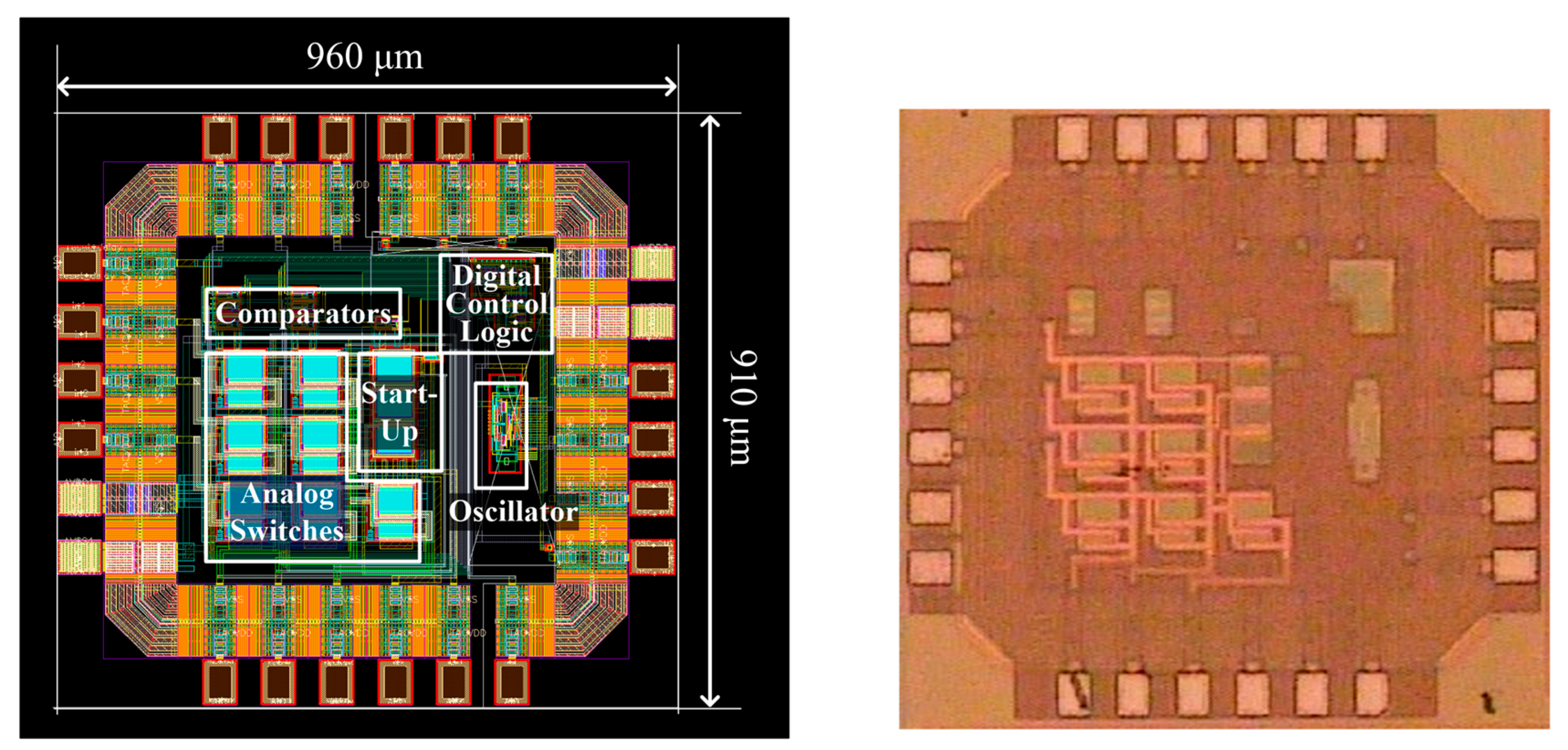
The proposed energy management circuit with dual outputs was designed and fabricated using a 0.13 µm TSMC CMOS technology. A layout and a die micrograph are shown in Figure 9, and the die size was 960 × 910 µm. An I/O pad with minimum leakage power and capacitance was selected to reduce power consumption. The newly developed IC was packaged with 4 × 4 mm quad-flat no-leads (QFN) with 24 leads. When all input ports were enabled, the power consumption of the packaged IC was just 1.5 µW with 1.2 Vdd. The frequency of the internal oscillator was 32 kHz, and the digital control circuit checked the state of the input harvester every 125 µs.
To measure the functional operation of the newly developed IC, an evaluation board was designed with three input ports. Each harvester was modeled with a power supply. The capacitance of each input was 10 nF. The load in a low-power path was modelled with a resistor to consume power of 55 µW. The power more than 55 µW was supplied to a high-power path, and charged a battery. The battery in a high-power path was modelled with a small size resistor to consume much more power than the load in the low-power path. In this experiment, the power consumption of the battery in high power was set up at five times of that of the load in low-power path (275 µW). To show the functionality of the energy management circuit described in previous section, three types of experiment was tested, and the waveforms were acquired with four channel digital oscilloscope. The first experiment was conducted to show the internal operating waveforms of the IC with one energy harvester. The second experiment shows the waveforms of dual outputs according to the magnitude of input harvesting energy in case of multi-source energy harvesters. In the last experiment, power distributing ratio between low-power path and high-power path and the energy combining efficiency from multi-source energy harvesters in the developed IC is depicted as the magnitude of the input harvesting energy.
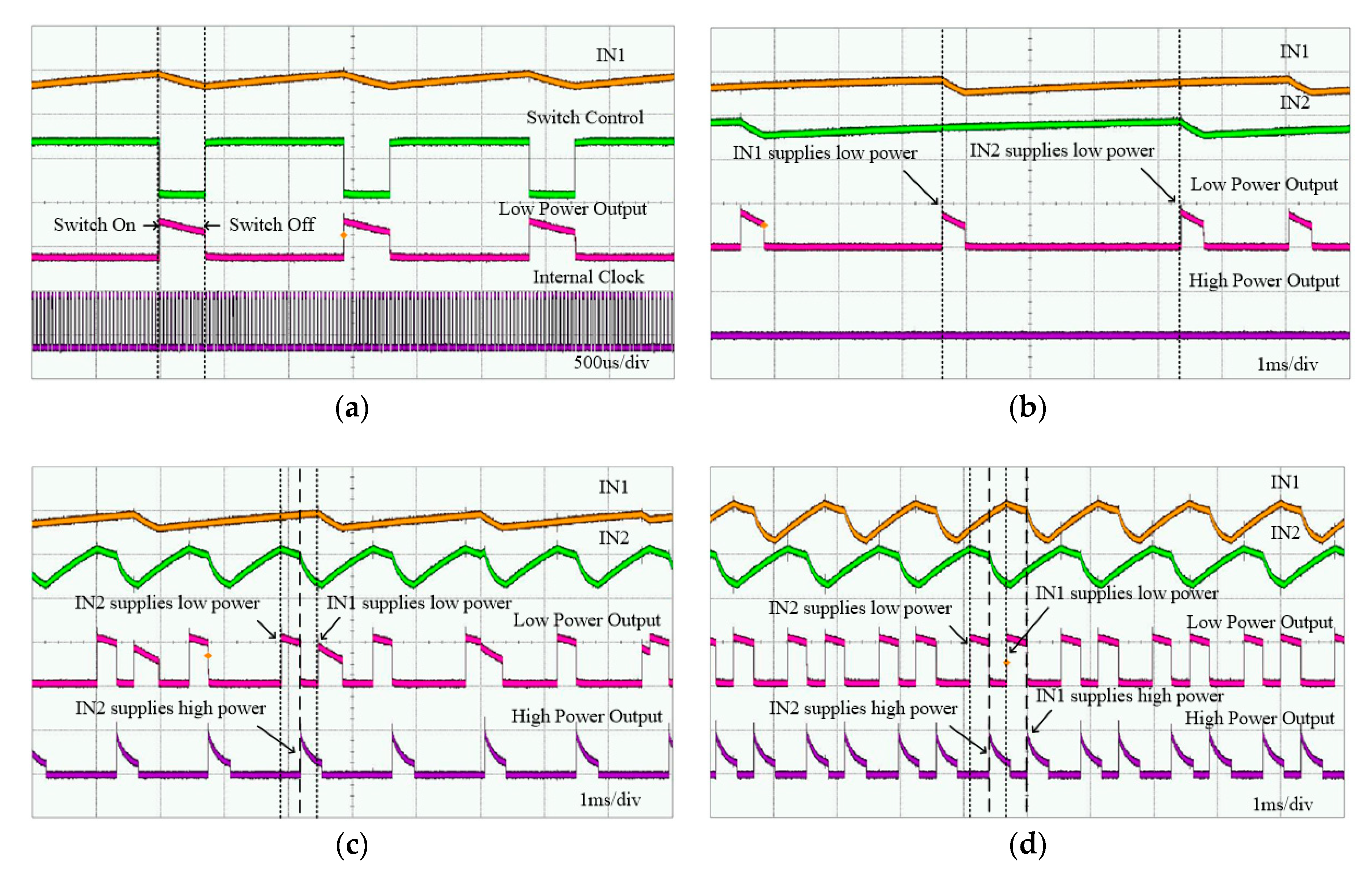
The first experiment involved a single energy harvester. The waveforms for the experiment are shown in Figure 10a. When an input energy harvester in low state starts to generate energy, the voltage of the input capacitor increases to the threshold voltage, Vth. The frequency of an internal oscillator can be tuned by changing the bias voltage with an external resistor. In this experiment, the internal oscillator generated a 32 kHz clock signal with a 10 MΩ bias resistor. With a 32 kHz internal clock, the digital control logic checked the input capacitor voltage in every 125 µs. If the voltage of the input capacitor was higher than the Vth, the digital control logic turned off the low-power path switch, and the energy stored in the input capacitor was supplied to a load on a low-power path. While supplying the energy in the input capacitor to a load, the input capacitor discharges. Therefore, the input capacitor is repeatedly charged and discharged near the Vth level, and at the load stage, the harvested power is available at times. According to the magnitude of the input power harvested, the duty rate at a load stage can change. With high harvest power, the on-time for a switch increases, and with low harvest power, the time becomes shorter.
The next experiment was done to show the output path transition from a low-power path to a high-power path as the magnitude of input harvested energy increased using multi-source harvesters. The experiment was conducted with two energy harvesters because of the limitation of channel number in the oscilloscope. The waveforms with multi-source energy harvesters are depicted in Figure 10b–d. If the first and the second energy harvesters generate less power than that consumed by the load in the low-power path (55 µW); both energy harvesters supply energy to the load in the low-power path at the same time by allocating time to each harvester as shown in Figure 10b. If two energy harvesters supply energy at the same time, the time to supply power to the load in the low-power path becomes twice the time for a single energy harvester. This means that the energy supplied is doubled with two energy harvesters. If the power of the second energy harvester increases to more than the power consumed at the load on the low-power path (55 µW), the first energy harvester still supplies power to the load on the low-power path and the second energy harvester sometimes goes to the high-power path. Then the second harvester supplies power to a battery in a high-power path as shown in Figure 10c. If the power of the second energy harvester is higher than the power consumed in a high-power path, the second harvester maintains the energy supply to the battery in a high-power path. However, in this experiment, the harvested power in the second harvester was not higher than the power consumption from the battery, and the voltage of the second capacitor dropped. Therefore, next time, the second harvester supplied power to the load on the low-power path again. If the powers of the first and the second energy harvester increase upper than the power consumed at the load on the low-power path, the first and the second energy harvesters supplied power to the load in the low-power path and a battery in high-power path at the same time as shown in Figure 10d.
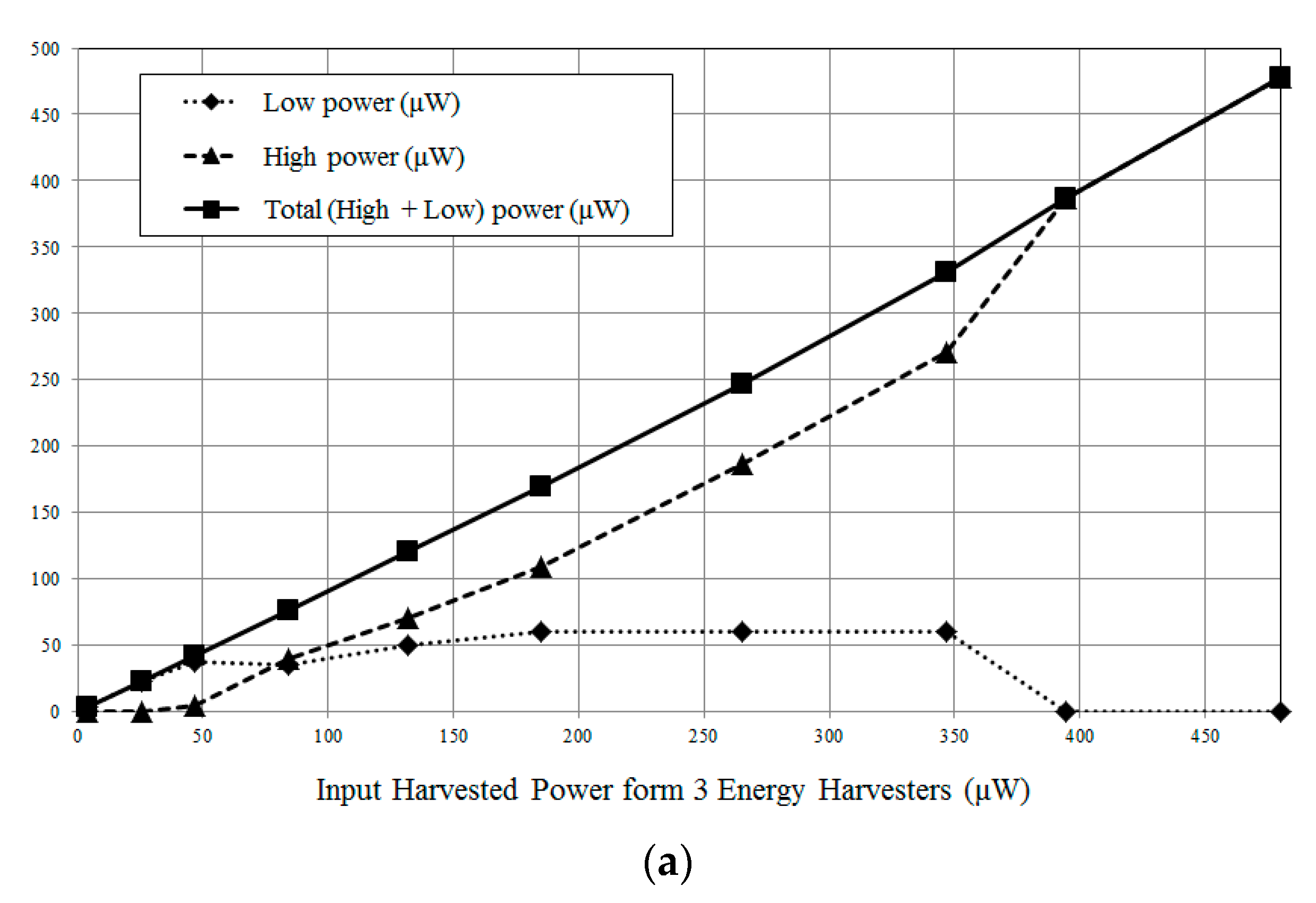
The graphs for the last experiment are depicted in Figure 11. When total harvested power from three harvesters is under 55 µW, all the energy is supplied through the low-power path. As the harvested power increases, some portion of the harvested energy starts to be supplied to a battery on the high-power path. The power supplied to a battery on the high-power path continues to increase as the harvested power increases. When the harvested power is 350 µW, the power supplied to both of output paths is 330 µW; whereas, 55 µW is supplied to a load on the low-power path, and 275 µW is supplied to a battery on the high-power path. If the harvested power is more than 350 µW, the energy supplied through the low-power path is stopped, and all the energy is supplied to a battery on the high-power path, and all input energies are stored into the battery. The battery can supply the energy required at the load on the low-power path. When the harvested energy is excessively higher than the energy required at the load, the voltage of temporary storage may rise rapidly. To keep the IC safe, the energy stored in the temporary storage should be transferred as soon as possible. With a higher energy consumption on the high-power path, input harvested energies are assigned only to the high-power path at all times.
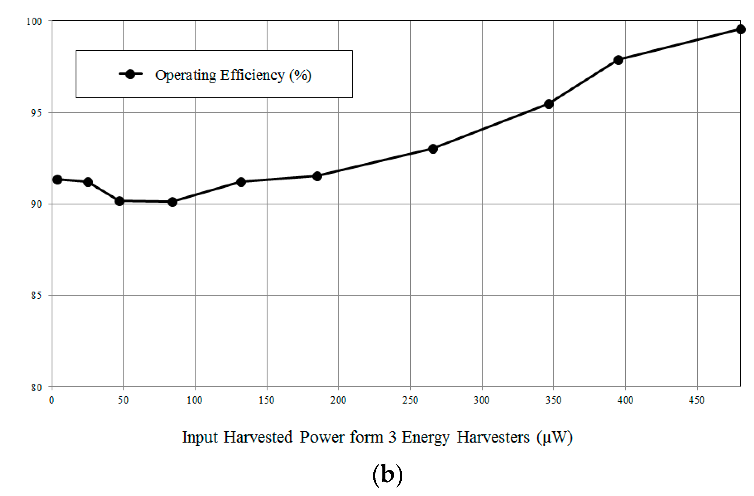
The efficiency is derived from the ratio between the total power supplied to a load and total power harvested by the three harvesters. Generally, with the constant power consumption of the IC, as the harvested power increases, the efficiency improves. However, if the harvested power becomes excessively high, the resistance of the path switch may affect the efficiency, and the overall efficiency might decrease. During measurement, in the harvest-energy range 50–480 µW, the efficiency was sustained at over 90%, and continuously increased. When under 50 µW, a slightly higher efficiency occurred, which is considered characteristic of this process. Maximum power loss occurred, when 265 µW of power was harvested. At that point, the efficiency was 93%, and total power loss was 18.5 µW. However, the power loss was a very small when compared to the power loss with the conventional OR-ing method, with which more than half the power may be wasted according to the operating conditions.
6. Discussion
There is now great interest in autonomous WBANs with renewable energy sources. Autonomous WBANs could get energy from their surrounding environment and use it to charge a battery. Autonomous WBANs are a very important technology, especially for use in implantable devices for which it is hard to maintain a battery. However, the energy obtained from most harvesters is limited to micro watt scale. To obtain significant amounts of energy from harvesters, technology for combining the energy from multiple harvesters is essential. In recent research on WSNs, a multi-source energy harvesting platform or modular unit with a micro-processor was proposed [17,18,19]. In this work, an energy management circuit that includes analog and digital parts was fabricated using a 0.13 µm TSMC CMOS technology. In WBANs, the IC solution may be a major feature when considering the size, weight, and lifetime of wearable devices. With the newly developed IC, power consumption was minimized to 1.5 µW with 1.2 Vdd when combining the energy streams from three harvesters with more than 90% efficiency. With the power consumption that occurs when combining energy, it is advantageous to regulate and supply energy to a load after combining the energy from multi-source energy harvesters.
In applications with multi-source energy harvesters, various kinds of energy harvesters might be adopted, and the energy streams generated from various kinds of harvesters should be combined. Every kind of harvested energy has a different form and standards do not yet exist. According to the type of transducers, DC or AC power can be generated. The harvested energy in PV cells is DC type, and that in PZs cells is AC type. The proposed IC only manages DC power. When AC power is generated from an ambient energy harvester, a rectifier circuit is required in front of the IC as derived in [20,21,22]. Much research has been done to improve the efficiency of rectifier and multiplier circuits, and in [23], a CMOS solution in a rectifier with a 0.18 µm technology was also implemented. In low-power applications such as WBANs, if possible, the energies from multi-harvesters have to be combined effectively prior to doing other work. When the magnitude of energy becomes sufficient to be utilized by the electronic systems, the output voltage should be converted to a regulated voltage level suitable for a load device by an additional interface circuit. This is because it is not easy to change the output voltage with very small amounts of energy. By combining the low energy in harvesters, this study shows the potential for utilizing low-power harvesters. Energy sources that were thought useless previously can now be utilized in electronic devices and can be commercialized.
The power consumption in electronic devices has been decreased continuously. There are now many applications that can operate with low power consumption such as mesh networks [24], sensor and control systems, RF identification (RFID) devices, and MEMS [25]. As an example of wearable applications, several types of energy harvesters can be attached to the clothes. PZs utilize vibrations from body movement and TEGs utilize temperature difference between body and air. All of these attached transducers concurrently generate electrical energy from every day behavior and could provide energy to a wearable sensor network. By adopting multiple inputs and multiple load schemes, the harvested energy could allow network modules to communicate. The system can only be made autonomous with multiple low-power energy harvesters. If the energy harvested on clothes is not sufficient to operate the network as a primary energy source, it could still play a role as a secondary energy source with a battery. The battery would be the main energy supply for the network, while the harvested energy would extend the battery life.
Today, energy harvesters have difficulty in commercialization because of their low efficiency and small amount of energy harvested. Photovoltaic (PV) cells to harvest the energy in sunlight are considered the only harvester commercialized as a field of industry. Fortunately, the amount of energy provided can be overcome by using multiple energy sources as described above. For their use in autonomous systems, the improvement of efficiency in energy harvesters remains a challenge. Various types of energy sources suitable for use in WBAN wearable devices should be surveyed. From the technology proposed herein, low energy harvesters can be considered practical energy sources, and more energy sources in or around the human body are worth investigating.
In future, more wearable devices will be installed inside and outside of human bodies for health monitoring and more convenient living. Such wearable devices will require more energy from the environment surrounding them. Energy harvesters and energy management technology are expected to be the most feasible solutions for supplying energy to wearable devices. In the near future, based on energy harvesting systems, disengaging wearable devices from the limitation of battery life is expected to be realized.
7. Conclusions
In this paper, an effective energy management circuit for combining energy from multi-source harvesters and distributing the harvested energy to dual loads is presented. By combining energy harvested from multi-source harvesters, the small amount of energy harvested in each harvester is overcome. The restrictions in the availability of each energy harvester due to the small amount of energy harvested is alleviated, and the system reliability is improved. By adopting a dual output scheme, a load and a rechargeable battery can be accommodated at the same time, and a wide range of levels of harvested energy is handled. When the input harvesters provide more energy than required by the load, the extra energy goes into a rechargeable battery and is thereby conserved safely. The extra energy used to charge the battery can be utilized by a load after a sufficient amount accumulates.
The proposed energy management circuit is integrated using a 0.13 µm TSMC CMOS technology. The die size is 960 × 910 µm. The newly developed IC includes analog and digital circuits based on ultra-low-power schemes. With a simple structure, the system monitors the magnitude of harvested energy and effectively combines the energy from each harvester. An evaluation board was designed and tested to obtain the measurement results. Each harvester was externally modeled, and the threshold powers were set at 55 and 275 µW for low power and high power, respectively. When all the sources were enabled, the operating power consumption of the IC was 1.5 µW with 1.2 Vdd. The frequency of the internal oscillator was 32 kHz, and the digital control circuit checked the state of the input harvester every 125 µs. The new technique used a novel algorithm to combine and distribute energy to dual loads. The adopted algorithm decides which output should be connected to a load based on the present and previous state of harvested energy. The proposed algorithm enables all the attached energy harvesters to have the same chance to supply energy to a load. The energy management efficiency is more than 90% over the whole range of input power.
In WBANs, it is hard to combine energy from multi-source energy harvesters. The conventional diode OR-ing scheme has a forward voltage drop, and the inductor sharing dc-dc converter scheme is hard to employ with micro watt energy harvesters because of the power consumed by the IC. The newly developed IC is suitable for many critical low-power applications with multiple and multi-type energy harvesters. By combining energy streams from very limited power sources with high efficiency, it can provide an effective solution for powering autonomic systems such as wearable devices or WBANs.
Author Contributions
Conceptualization, H.-I.P. and I.G.L.; Methodology, T.K.; Simulations, M.J.P. and J.-J.L.; Measurements, K.-I.O.; Original Draft Preparation and Supervision, S.-E.K.
Funding
This work was supported by Electronics and Telecommunications Research Institute (ETRI) grant funded by the Korean government (18ZB1200, Development of Core Technologies for Implantable Active Devices).
Conflicts of Interest
The authors declare no conflict of interest.
References
- Ottman, G.K.; Hofmann, H.F.; Lesieutre, G.A. Optimized piezoelectric energy harvesting circuit using step-down converter in discontinuous conduction mode. IEEE Trans. Power Electron. 2003, 18, 696–703. [Google Scholar] [CrossRef] [Green Version]
- Celik, T.; Kusetogullari, H. Solar-powered automated road surveillance systems for speed violation detection. IEEE Trans. Ind. Electron. 2010, 57, 3216–3227. [Google Scholar] [CrossRef]
- Li, W.; He, S.; Yu, S. Improving power density of a cantilever piezoelectric power harvester through a curved L-shape proof mass. IEEE Trans. Ind. Electron. 2010, 57, 868–876. [Google Scholar] [CrossRef]
- Mehraeen, S.; Jagannathan, S.; Corzine, K.A. Energy harvesting from vibration with alternate scavenging circuitry and tapered cantilever beam. IEEE Trans. Ind. Electron. 2010, 57, 820–830. [Google Scholar] [CrossRef]
- Wang, Z.; Leonov, V.; Fiorini, P.; van Hoof, C. Realization of a wearable miniaturized thermoelectric generator for human body applications. Sens. Actuators A Phys. 2009, 156, 95–102. [Google Scholar] [CrossRef]
- Dini, M.; Filippi, M.; Costanzo, A.; Romani, A.; Tartagni, M.; del Prete, M.; Masotti, D. A Fully-Autonomous Integrated RF Energy Harvesting System for Wearable Applications. In Proceedings of the 2013 European Microwave Conference, Nuremberg, Germany, 6–10 October 2013; pp. 987–990. [Google Scholar]
- Du, L.; Wang, C.; Li, X.; Yang, L.; Mi, Y.; Sun, C. A novel power supply of online monitoring systems for power transmissions lines. IEEE Trans. Ind. Electron. 2010, 57, 2889–2895. [Google Scholar]
- Mitcheson, P.D. Energy harvesting for human wearable and implantable bio-sensors. In Proceedings of the 2010 Annual International Conference of the IEEE Engineering in Medicine and Biology, Buenos Aires, Argentina, 31 August–4 September 2010; pp. 3432–3436. [Google Scholar]
- Ferrari, M.; Ferrari, V.; Guizzetti, M.; Marioli, D.; Taroni, A. Piezoelectric multifrequency energy converter for power harvesting in autonomous microsystems. Sens. Actuators A Phys. 2008, 142, 329–335. [Google Scholar] [CrossRef]
- Carli, D.; Brunelli, D.; Benini, L.; Ruggeri, M. An effective multisource energy harvester for low power applications. In Proceedings of the 2011 Design, Automation & Test in Europe, Grenoble, France, 14–18 March 2011; pp. 1–6. [Google Scholar]
- Tan, Y.K.; Panda, S.K. Energy Harvesting from Hybrid Indoor Ambient Light and Thermal Energy Sources for Enhanced Performance of Wireless Sensor Nodes. IEEE Trans. Ind. Electron. 2011, 58, 4424–4435. [Google Scholar] [CrossRef]
- Kang, T.W.; Kim, S.E.; Hyoung, C.H.; Kang, S.W.; Park, K.H. An energy combiner for multi-input energy harvesting system. IEEE Trans. Circuits Syst. II Exp. Briefs 2015, 62, 911–915. [Google Scholar] [CrossRef]
- Bakin, E.; Ivanov, I.; Shelest, M.; Turlikov, A. Analysis of Energy Harvesting Efficiency for Power Supply of WBAN Nodes in Heterogeneous Scenarios. In Proceedings of the 8th International Congress on Ultra Modern Telecommunications and Control Systems and Workshops (ICUMT), Lisbon, Portugal, 18–20 October 2016. [Google Scholar]
- Akhtar, F.; Rehmani, M.H. Energy Replenishment Using Renewable and Traditional Energy Resources for Sustainable Wireless Sensor Networks: A Review. Renew. Sustain. Energy Rev. 2015, 45, 769–784. [Google Scholar] [CrossRef]
- Hu, F.; Cai, Q.; Liao, F.; Shao, M.; Lee, S.T. Recent Advancements in Nanogenerators for Energy Harvesting. Small 2015, 11, 5611–5628. [Google Scholar] [CrossRef] [PubMed]
- Wang, W.S.; O’Donnell, T.; Ribetto, L.; O’Flynn, B.; Hayes, M.; O’Mathuna, C. Energy harvesting embedded wireless sensor system for building environment applications. In Proceedings of the 2009 1st International Conference on Wireless Communication, Vehicular Technology, Information Theory and Aerospace & Electronic Systems Technology, Aalborg, Denmark, 17–20 May 2009; pp. 36–41. [Google Scholar]
- Le, T.N.; Vo, T.P.; Due, A.V.D. Plug-In Multi-Source Energy Harvesting for Autonomous Wireless Sensor Networks. In Proceedings of the 2017 International Conference on Advanced Computing and Applications (ACOMP), Ho Chi Minh City, Vietnam, 29 November–1 December 2017; pp. 105–108. [Google Scholar]
- Ding, C.; Heidari, S.; Wang, Y.; Liu, Y.; Hu, J. Multi-Source In-Door Energy Harvesting for Non-volatile Processors. In Proceedings of the 2016 IEEE International Symposium on Circuits and Systems (ISCAS), Montreal, QC, Canada, 22–25 May 2016. [Google Scholar]
- Alhawari, M.; Tekeste, T.; Mohammead, B.; Saleh, H.; Ismail, M. Power Management Unit for Multi-Source Energy Harvesting in Wearable Electronics. In Proceedings of the IEEE 59th International Midwest Symposium on Circuits and Systems (MWSCAS), Abu Dhabi, UAE, 16–19 October 2016. [Google Scholar]
- Ashry, A.; Sharaf, K.; Ibrahim, M. A simple and accurate model for RFID rectifier. IEEE Syst. J. 2008, 2, 520–524. [Google Scholar] [CrossRef]
- Curty, J.P.; Joehl, N.; Dehollain, C.; Declercq, M. Remotely powered addressable UHF RFID integrated system. IEEE J. Solid-State Circuits 2005, 40, 2193–2202. [Google Scholar] [CrossRef]
- Yao, Y.; Shi, Y.; Dai, F.F. A novel low-power input-independent MOS AC/DC charge pump. In Proceedings of the IEEE International Symposium on Circuits and Systems, Kobe, Japan, 23–26 May 2005; pp. 380–383. [Google Scholar]
- Yi, J.; Ki, W.; Tsui, C. Analysis and design strategy of UHF micro-power CMOS rectifiers for micro-sensor and RFID applications. IEEE Trans. Circuits Syst. I Reg. Pap. 2007, 54, 153–166. [Google Scholar] [CrossRef]
- Gungor, V.C.; Hancke, G.P. Industrial wireless sensor networks: Challenges, design principles, and technical approaches. IEEE Trans. Ind. Electron. 2009, 56, 4258–4265. [Google Scholar] [CrossRef]
- Ting, Y.; Hariyanto, G.; Hou, B.K.; Ricky, S.; Amelia, S.; Wang, C.-K. Investigation of energy harvest and storage by using curve-shape piezoelectric unimorph. In Proceedings of the 9 IEEE International Symposium on Industrial Electronics, Seoul, Korea, 5–8 July 2009; pp. 2047–2052. [Google Scholar]
Figure 1.
Energy management for a wireless body area network (WBAN).

Figure 2.
Conventional architecture of a multi-source energy harvester.

Figure 3.
Architecture for a single-source energy harvester with the proposed energy management circuit.
Figure 3.
Architecture for a single-source energy harvester with the proposed energy management circuit.

Figure 4.
Energy flow according to the magnitude of energy harvested in the proposed energy management circuit. (a) 3 low powers; (b) 2 low powers and 1 high power; (c) 1 low power and 2 high powers; (d) 3 high powers.
Figure 4.
Energy flow according to the magnitude of energy harvested in the proposed energy management circuit. (a) 3 low powers; (b) 2 low powers and 1 high power; (c) 1 low power and 2 high powers; (d) 3 high powers.

Figure 5.
State classification for the harvest energy input.

Figure 6.
Low power analog blocks: (a) analog path switches; (b) comparators; and (c) oscillator.

Figure 7.
Flowchart for the process of the proposed algorithm.

Figure 8.
Block diagrams for the digital control logic. (a) trigger signal generator; (b) control signal generator for low power switch; (c) control signal generator for high power switch.
Figure 8.
Block diagrams for the digital control logic. (a) trigger signal generator; (b) control signal generator for low power switch; (c) control signal generator for high power switch.

Figure 9.
Layout and die micrograph of the energy management IC.

Figure 10.
Energy managing waveforms in the newly developed IC. (a) Internal waveforms in EMIC with one energy harvester; (b) IN1: low power, IN2: low power; (c) IN1: low power, IN2: high power; (d) IN1: high power, IN2: high power.
Figure 10.
Energy managing waveforms in the newly developed IC. (a) Internal waveforms in EMIC with one energy harvester; (b) IN1: low power, IN2: low power; (c) IN1: low power, IN2: high power; (d) IN1: high power, IN2: high power.

Figure 11.
Measured graphs for the newly developed IC. (a) measured-output flow as the magnitude of power; (b) operating efficiency as the magnitude of power.
Figure 11.
Measured graphs for the newly developed IC. (a) measured-output flow as the magnitude of power; (b) operating efficiency as the magnitude of power.


© 2018 by the authors. Licensee MDPI, Basel, Switzerland. This article is an open access article distributed under the terms and conditions of the Creative Commons Attribution (CC BY) license (http://creativecommons.org/licenses/by/4.0/).
Share and Cite
MDPI and ACS Style
Kim, S.-E.; Kang, T.; Oh, K.-I.; Park, M.J.; Park, H.-I.; Lim, I.G.; Lee, J.-J. Energy Management Integrated Circuit for Multi-Source Energy Harvesters in WBAN Applications. Appl. Sci. 2018, 8, 1262. https://doi.org/10.3390/app8081262
AMA Style
Kim S-E, Kang T, Oh K-I, Park MJ, Park H-I, Lim IG, Lee J-J. Energy Management Integrated Circuit for Multi-Source Energy Harvesters in WBAN Applications. Applied Sciences. 2018; 8(8):1262. https://doi.org/10.3390/app8081262
Chicago/Turabian StyleKim, Sung-Eun, Taewook Kang, Kwang-Il Oh, Mi Jeong Park, Hyung-Il Park, In Gi Lim, and Jae-Jin Lee. 2018. "Energy Management Integrated Circuit for Multi-Source Energy Harvesters in WBAN Applications" Applied Sciences 8, no. 8: 1262. https://doi.org/10.3390/app8081262
Note that from the first issue of 2016, this journal uses article numbers instead of page numbers. See further details here.