Abstract
InGaN/GaN samples grown on c-plane sapphire substrate with different In concentrations by metal organic chemical vapor deposition are demonstrated. The subsequent capping GaN layer growth opens a possibility for dislocation reduction due to the lateral strain relaxation in growth geometry. We present the further growth optimization and innovative characterization of InGaN layers overgrown on different structures with varying In concentrations. The photoelectrical and optical properties of the InGaN layers with/without capping GaN layer are investigated by time-resolved picosecond transient grating and temperature dependence photoluminescence. We note a 10-fold increase in carrier lifetime in the InGaN layers when the sample structure changed from PIN to single InGaN layer.
1. Introduction
The use of photovoltaic devices is attractive due to the high global energy demands and the abundance, cleanliness, and renewability of solar energy. Among semiconductors, group III nitrides feature excellent potential as replacements for traditional photovoltaic absorption materials in high-efficiency solar-cell production [1,2,3,4,5,6]. The direct energy gap of the InxGa1−xN system can be adjusted by optimizing In composition to absorb the entire solar spectrum [7]. Excellent physical features, such as high mobility, drift velocity, radiosity, thermal conductivity, and high-temperature resistance, result in prolonged lifetime and strong light absorption, rendering InGaN alloys as possible substitutes for traditional solar cell absorbents [7,8]. Si solar cells may be affected by unstable operation, whereas InGaN-based solar cells possess the potential to operate smoothly in harsh environments [5]. Zhang et al. calculated the conversion efficiency of group III nitride photovoltaic devices in 2007 [9] and recorded the efficiency of a single In0.65Ga0.35N battery at a value of up to 20%. InGaN/GaN, as a battery interface, increases efficiency up to 35.1% [10]. Under a similar operating background, Hsu et al. [11] improved the efficiency of InGaN/Si series solar cells by 35% using two InGaN junctions. Theoretically, the efficiency of multi-junction solar cells increases with additional junctions, whereas that of a series of solar cells containing eight stacked layers can reach 56% [2]. Although these characteristics present broad prospects, the performance of solar cells using InGaN must be considerably improved owing to their low conversion efficiency [2,12]. The performance of InGaN solar cells is hindered by structural degradation of thick InGaN layers. Alloys possess a high In content (>10%) owing to the dislocation and relaxation caused by inhomogeneity and vacancy-related defects [13,14]. The limitations of a thick InGaN layer are overcome by the use of multiple quantum wells (MQWs) or a superlattice absorbing layer in solar cells to limit the accumulation of stress and control defect formation. Compared with solar cells manufactured using a thick InGaN-absorbing layer [2,15,16], MQW structures improve the crystallinity and performance of solar cell devices. The performance of InGaN MQW solar cells can be further improved by increasing the number of quantum wells and thickness of the active region [13,17,18]. However, the loss of collecting carriers and the increase in MQW region composition result in the saturation of a large number of quantum wells by short-circuit currents [19]. Therefore, photon absorption in InGaN MQW active regions for photovoltaic applications can be strengthened by developing new structures that can achieve large InGaN active regions.
Nonlinear four-wave mixing (FWM) technology is becoming a general tool for describing a large number of crystals and micron-scale semiconductor and nanostructures. FWM can quickly and reliably evaluate new photoelectric materials and related technologies. This technology enables multiple electrical parameter measurement of semiconductors in an all-optical manner on the basis of correlations between electrics and optics. The unique advantage of FWM is its capability to directly analyze transmission of carriers by changing the interval of optical interference patterns. Previous studies on InGaN materials using FWM technology were carried out based on heterostructure and single quantum well samples [20,21,22]. Okamoto et al. [20] have proven that the considerable decrease in external quantum efficiency (ηext) of light-emitting diode in InGaN refers not to the increase in non-radiative composite centers but the carrier delocalization caused by rapid diffusion. In previous studies, we proposed a free carrier grating decay time with different spatial periods to determine the bipolar diffusion coefficient, D = 2.1 cm2/s, with 470 ps effective carrier life for estimating the corresponding 40 cm2/Vs hole mobility and 1018 cm−3 density of the carrier [21]. Time-resolved-FWM (TR-FWM) and photoluminescence (PL) technologies are used to study the dynamics of the disequilibrium carrier and the competition of non-radiative and radiative recombination in different InxGa1−xN-doped heterostructures to further describe the correlation between photoelectric transmission and structural characteristics of InGaN alloy [22].
In this study, we optically analyzed InGaN/GaN samples grown on sapphire with different In concentrations and capping layers. The grown structures were evaluated using time-integrated luminescence and TR-FWM techniques. Section 2 discusses the growth conditions and experimental procedures. Section 3 presents the X-ray diffraction (XRD), temperature dependence (PL), and TR-FWM results. Finally, Section 4 provides the conclusions drawn from the study.
2. Sample Structures and Experimental Procedures
In this study, four different InxGa1−xN/GaN samples were grown using metal organic chemical vapor phase deposition. We performed the following steps to grow sample SI27. First, we purified the sapphire substrate at 1800 °C, applied nitride to the surface, and grew a thin (2 µm) GaN layer at 530 °C. Second, we grew a 200 µm thick layer of In0.27Ga0.73N at 650 °C. Then, we improved the joining between the In0.27Ga0.73N and GaN layers at 580 °C. CSI27 is a GaN layer with a growth thickness of 120 nm and a growth temperature of 530 °C on SI27. For sample PIN27, the growth steps were as follows. First, we purified the sapphire substrate at 1800 °C, applied nitride to the surface, and grew a thin (1.5 µm) GaN layer at 530 °C. Then, we grew doped Si at 550 °C to form an N-type GaN layer with a thickness of 500 nm. Next, we grew the In0.27Ga0.73N layer at 650 °C. Afterward, we improved the joining between the In0.27Ga0.73N and GaN layers at 580 °C. Eventually, we grew doped Mg at 550 °C to form a P-type GaN layer with a thickness of 120 nm. Finally, we improved the joining between the In0.27Ga0.73N and P-type GaN layers at 580 °C. The growth conditions of sample PIN 15 were similar to those of sample PIN27, except that the In concentration was changed to 15%. Figure 1 shows the structures of the four samples.
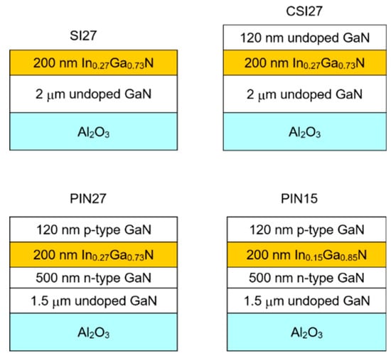
Figure 1.
Scheme of InGaN/GaN sample structures used in this work.
Carrier dynamics in InGaN/GaN samples were investigated using picosecond FWM. Temperature-dependent PL measurement was carried out through exciting 325 nm light using 50 mW He–Cd laser. Carrier flow dynamics in InGaN/GaN samples were studied using picosecond FWM [23,24,25,26,27]. The set-up shown in Figure 2 was used to perform a TR-FWM experiment. Different materials were measured using varying wavelengths to excite light from the carrier. A mode-locked picosecond YAG:Nd laser (PL2143 type, Ekspla) or various resonant waves from an optical numerical generator (PG401, Ekspla) were used as light source. The pump wavelengths provided by the set-up were 532, 355, and 266 nm, and the pulse energies were 15, 10, and 5 mJ, respectively. The initial beam diameter measured 1–2 mm for grating recording. The numerical generator could be adjusted in the spectrum ranges of 420–680 and 740–2000 nm. The maximum pulse energy at 500 nm was approximately 1 mJ. In the present study, the first resonant wave of most experimental lasers at 1064 nm was used as a probe beam, which ensured the highest sensitivity of non-resonant refractive index modulation for free carriers. The 355 nm picosecond numerical generator was used as pump beam for recording instantaneous free carrier grating in InGaN layer and preventing light absorption in the GaN layer. Attenuation was controlled, and pulse energy of the beam was recorded by rotating a λ/2 plate in front of the grand prism. The optical path difference of interfering beams can be adjusted using a short step-driven pump delay line to allow a delay time adjustment of up to 1.5 ns. Incident beam energy was measured using an energy detector, and spatial profile of the beam was controlled by a charge-coupled device line. Five measurements were performed with fixed probe beam delay at time Δt, and data were integrated at the intensity window required for I0 ± ∆I0 (usually, ΔI0/I0 < 5%) to measure the grating attenuation dynamics. The exposure characteristics under different levels of excitation energy were measured by collecting 500–1000 times of laser irradiation. LabVIEW data acquisition system was used to monitor experimental and data processing, and time showed the measured FWM characteristics. A holographic spectroscope (HBS) was used to divide the pump beam into two beams to form dynamic grating in the sample. Two interfering beams generated against HBS were used to construct simple temporal and spatial adjustments, which enabled easy adjustment of the dynamic grating period by replacing HBS with another grating with different spacing. This new FWM tool is commonly used, reproducible, and easy to operate. In the experimental set-up shown in Figure 2, θ refers to the angle between two incident beams in a pump beam. Another study showed other details of non-degenerate ps FWM using HBS components [27]. Excitation of crystal-free carrier gratings with optical interference patterns shows advantages over those of other probe excitation techniques. Given the temporal and spatial modulation of optical properties of matter by incident light I(x) = I0 [1 + cos(Kx)], the disequilibrium carrier current distribution of spatial modulation was generated N(x,t) = N0(t) + ΔN(x,t) cos(Kx), where N0 and ΔN refer to unmodulated and modulated carrier densities, respectively, along the grating vector K = 2π/Λ with the cycle of Λ. Free carrier gratings were generated by repeating the modulation of instantaneous electrical properties by the modulation values Δn(x,t)~ΔN(x,t) with refractive index n [28]. The time interval of beam detection corresponded to the delay in grating efficiency of η(t)~exp(), which paralleled the time interval of probe beam , in which the η value decreased by e2, whereas carrier modulation decreased by e in this interval. Similar sampling was repeated in other grating periods, and the corresponding τG value was determined. The plot of inverse grating decay time versus (or the so-called angular dependence of decay time) determined the diffusion coefficient and carrier recombination time. One of the first two parameters was determined by the grating period, as shown below:
where denotes the recombination time, and τD = Λ2/(4π2D) indicates the diffusion time of the grating erasure.
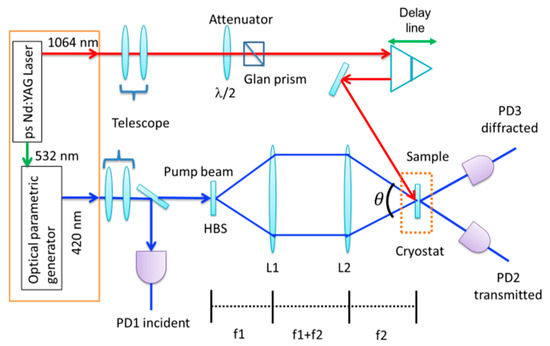
Figure 2.
Optical scheme of nondegenerate four-wave mixing (FWM) with holographic spectroscope (HBS) as beam splitter.
3. Results and Discussions
3.1. Band Gap of InGaN
Recognizing that the energy gap of InGaN varies with In concentration is necessary for the design of an InGaN-based optical power supply to obtain high-efficiency luminescence with a target light wavelength from the InGaN layer. The change in the InGaN energy gap with In concentration is also an important issue in theoretical research. Unfortunately, the light emission of InGaN originates not from a uniform InGaN layer but from local structure due to In segregation, phase separation, and other reasons. These phenomena result in a considerably lower PL emission compared with the energy gap of the “carrier” InGaN layer and its unusability in obtaining the InGaN energy gap. In literature, the most common methods used to measure the energy gap of InGaN include absorption spectra [29,30], optical density measurements [31], and PL excitation spectra [32,33]. A discussion of energy gap bending parameters of InxGa1−xN as a function of x is underway. M. De Luca et al.reported a pertinent study regarding high-In-concentration InGaN samples [34]. Given the difficulty of the high-In-concentration growth of InGaN and pure In, the energy gap of InxGa1−xN with high x or x = 1 is rarely studied. Thus, the uncertainty of energy gap with high in concentration must be studied. Given the improved growth of h-InN, the effects of O and interfacial metal clusters can be avoided [35]. The InN energy gap has been measured and discussed in several papers. The new h-InN energy gap is in the range of 0.7–1.4 eV. Bechstedt et al. [36] calculated the InN energy gap of 0.58 eV. The sample we studied was an InGaN layer grown on a GaN buffer layer by using a sapphire (Al2O3) substrate. The energy gap of InGaN and In concentration was determined using eq (2) according to the reference [37]:
3.2. XRD Results
Figure 3 shows the ω-2θ line scan with different InxGa1−xN layers grown on sapphire (Al2O3) substrate. The peak of Bragg reflection from the GaN buffer layer showed the greatest intensity, whereas the arrows in the figure represent the InxGa1−xN peaks of four samples (i.e., SI27, CSI27, PIN15, and PIN27). SI27 exhibited a diffraction signal of In0.27Ga0.73N at 33.56°. Sample CSI27 showed a diffraction signal of In0.48Ga0.52N and In0.19Ga0.81N at 32.92° and 33.80°, respectively. PIN27 presented the diffraction signals of In0.47Ga0.53N and In0.2Ga0.8N at 32.94° and 33.78°, respectively. PIN15 exhibited the diffraction signal of In0.15Ga0.85N at 34.05°, whereas CSI27 and PIN27 produced two different crystal phases of InxGa1−xN. These findings are possibly attributable to the extremely high concentration of doped In. Hence, the concentration of a part of In was diffused into the uppermost layer of GaN, thereby resulting in two different crystal phases of InxGa1−xN. Table 1 presents the XRD measurement results of SI 27, CSI27, PIN27, and PIN15 according to equation (2). The InGaN peak shown in Figure 3 exhibited an increased distance from the GaN peak. All InGaN layers were characterized by pseudomorphicity on the GaN buffer layer. CSI27 and PIN27 exhibited two separate InxGa1-xN phase peaks detected from the InGaN/GaN scan in Figure 3. The tilt of the InGaN layer to the GaN buffer layer was absent in the four samples studied.
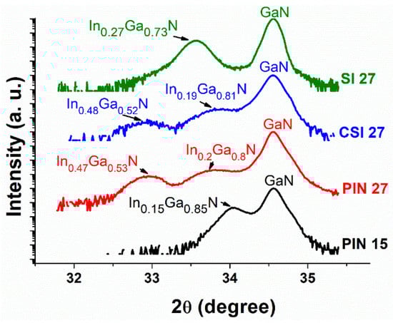
Figure 3.
XRD results of four samples.

Table 1.
Relationship between In concentration of InxGa1-xN and band gap.
3.3. PL Results
Figure 4 shows the temperature-dependent PL spectra of the samples. In SI27 (Figure 4a), the temperature-dependent PL peak energy exhibited no S-shape behavior. The S-shape behavior has been attributed to the carrier dynamics associated with carrier localization in potential minimums [23,24,25,38,39]. As shown in Figure 4b, two PL spectral peaks were identified below 150 K. The low-energy peak corresponded to localized states. The high-energy peak was attributed to free-carrier states, corresponding to the background InGaN compound on which clusters were distributed. However, the background InGaN compound also consisted of potential fluctuations of shallow distributions. The merging of PL peaks above 150 K was attributed to carrier liquidation among the localized states and free-carrier states. The decreasing trend of high-energy peak was mainly due to the band-gap shrinkage of phonon effect [40]. As shown in Figure 4c, the PL peaks showed broader bandwidth than the SI27 sample, indicating an evident In concentration fluctuation. As shown in Figure 4d, the PL peak position corresponded to low In concentration (~15%). The poor optical quality of PIN15 was due to the low emission energies existing between 450 and 500 nm.
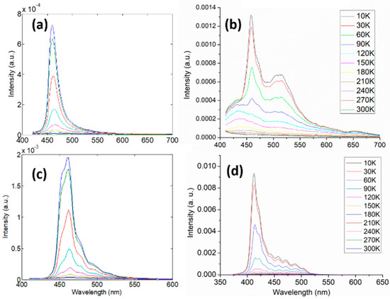
Figure 4.
Temperature-dependent photoluminescence (PL) spectra of samples (a) SI27, (b) CSI27, (c) PIN27, and (d) PIN15.
3.4. TR-FWM Results
Measurements were carried out at room temperature with various excitation energy densities I. Figure 5 shows the decay of light-induced transient grating (LITG) recorded in the samples. The decay kinetics were nearly exponential and occurred rapidly for small grating periods, in accordance with eq (1). The τR and D values were determined by plotting the dependence of grating decay rate 1/τG versus inverse grating period ∆N−2. Similarly, we measured the grating decay rates in InGaN layers grown on different In concentrations. Table 2 presents the determined parameters. The data indicated that lifetime decreased with excitation energy densities. CSI27 and PIN27 showed the longest carrier lifetimes and typical D values for InGaN. Complementary measurements of PL intensity at 325 nm excitation (Figure 4) demonstrated the increased radiative recombination component due to decreased nonradiative recombination rate in InGaN layers. The presence of a high density of defects in the used template may also influence the quality of InGaN layers. The extremely short carrier lifetime of about 150 ps in PIN27 and its approximately 10-fold increase with excitation reflected the high defect density and partial saturation of electron trapping centers by the injected carriers. In CSI27, four power measurement results were provided, thereby showing better quality than the other samples.
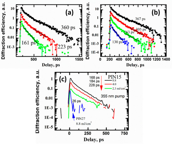
Figure 5.
FWM decay spectra with different excitation powers on (a) SI27, (b) CSI27, (c) PIN15, and PIN27, with the excitation powers of 8.8, 4.0, 2.3, and 1.5 mJ/cm2, respectively.
Table 2.
Carrier lifetime τR (ps) and diffusion coefficient D (cm2/s) in InGaN layers grown with different In concentrations (SI27, CSI27, PIN27, and PIN15).
4. Discussion
From the measurement results of FWM, numerous defects existed in sample PIN27. FWM can only monitor Da and τR values with excitation energy density I0 of 8.8 mJ/cm2. The values of Da and τR reached 2.73 cm2/s and 0.15 ns, respectively. Only one FWM measurement was observed given the remarkably high In doping concentration, whereas a number of high defects were generated in the P-type GaN layer. For sample PIN15, CSI27, and SI27, the values of Da and τR totaled 2.56 cm2/s and 0.45 ns, 1.83 cm2/s and 1.59 ns, and 1.73 cm2/s and 1.48 ns, respectively. Comparison of PIN15 with PIN27 revealed that as In content increased from 15% to 27%, the D value increased from 2.56 cm2/s to 2.73 cm2/s. The grating times of CSI27 and SI27 totaled τG = 1.59 ns and τG = 1.48 ns, respectively, with no significant difference. Finally, we integrated the XRD, PL, and FWM measurement results, mainly based on the results of FWM measurement of the quality of samples SI27, CSI27, PIN27, and PIN15. According to results, CSI27 showed the best performance, followed by SI27, PIN 27, and finally PIN15.
5. Conclusions
Using complementary optical techniques, we confirmed the improved electrical, optical, and structural parameters of InGaN layers in different In concentrations. CSI27 yielded an optimal carrier lifetime of 1.59 ps and diffusion coefficient D of 1.83 cm2/s. Sample quality increased in the capping GaN epilayer when the In concentration was 27%. This feature indicated an approximately twofold decrease in defect density. Low-efficiency electron trapping in overgrown GaN was supported by D = 1.6 cm2/s value, which was typical for bipolar plasma in GaN, whereas the D value was two times faster in the template (as n < p). Increasing lifetime value with excitation was typical for the saturation of electron trapping centers by excess carriers in InGaN with capping GaN structure.
Author Contributions
Z.T.Y. and H.-T.N. were responsible for data and optical measurements. H.-T.N. analyzed the XRD, PL, and FWM results. S.-W.F., Z.T.Y., H.-L.C., and H.-C.W. organized and wrote the manuscript.
Funding
This work was financially/partially supported by the Advanced Institute of Manufacturing with High-Tech Innovations from the Featured Areas Research Center Program within the framework of the Higher Education Sprout Project by the Ministry of Education in Taiwan.
Acknowledgments
This research was supported by the Ministry of Science and Technology, the Republic of China (grant No. MOST 106-2112-M-194-002), and Kaohsiung Armed Forces General Hospital research project 104-43.
Conflicts of Interest
The authors declare no conflict of interests.
References
- Wierer, J.J.; Li, Q.; Koleske, D.D.; Lee, S.R.; Wang, G.T. III-nitride core-shell nanowire arrayed solar cells. Nanotechnology 2012, 23, 194007. [Google Scholar] [CrossRef]
- Bhuiyan, A.G.; Sugita, K.; Hashimoto, A.; Yamamoto, A. InGaN solar cells: Present state of the art and important challenges. IEEE J. Photovolt. 2012, 2, 276–293. [Google Scholar] [CrossRef]
- Dahal, R.; Li, J.; Aryal, K.; Lin, J.Y.; Jiang, H.X. InGaN/GaN multiple quantum well concentrator solar cells. Appl. Phys. Lett. 2010, 97, 73115. [Google Scholar] [CrossRef]
- Mori, M.; Kondo, S.; Yamamoto, S.; Nakao, T.; Iwaya, M.; Takeuchi, T.; Kamiyama, S.; Akasaki, I.; Amano, H. Concentrating Properties of Nitride-Based Solar Cells Using Different Electrodes. Jpn. J. Appl. Phys. 2013, 52, 08JH02. [Google Scholar] [CrossRef]
- Lien, D.H.; Hsiao, Y.H.; Yang, S.G.; Tsai, M.L.; Wei, T.C.; Lee, S.C.; He, J.H. Harsh photovoltaics using InGaN/GaN multiple quantum well schemes. Nano Energy 2015, 11, 104–109. [Google Scholar] [CrossRef]
- Jung, B.O.; Bae, S.Y.; Kim, S.Y.; Lee, S.; Lee, J.Y.; Lee, D.S.; Kato, Y.; Honda, Y.; Amano, H. Highly ordered catalyst-free InGaN/GaN core–shell architecture arrays with expanded active area region. Nano Energy 2015, 11, 294–303. [Google Scholar] [CrossRef]
- Wu, J.; Walukiewicz, W.; Yu, K.M.; Shan, W.; Ager, J.W.; Haller, E.E.; Lu, H.; Schaff, W.J.; Metzger, W.K.; Kurtz, S. Superior radiation resistance of In1−xGaxN alloys: Full-solar-spectrum photovoltaic material system. J. Appl. Phys. 2003, 94, 6477–6482. [Google Scholar] [CrossRef]
- Meneghesso, G.; Verzellesi, G.; Danesin, F.; Rampazzo, F.; Zanon, F.; Tazzoli, A.; Meneghini, M.; Zanoni, E. Reliability of GaN high-electron-mobility transistors: State of the art and perspectives. IEEE Trans. Device Mater. Reliab. 2008, 8, 332–343. [Google Scholar] [CrossRef]
- Zhang, X.; Wang, X.; Xiao, H.; Yang, C.; Ran, J.; Wang, C.; Hou, Q.; Li, J. Simulation of In0.65Ga0.35N single-junction solar cell. J. Phys. D Appl. Phys. 2007, 40, 7335–7338. [Google Scholar] [CrossRef]
- Zhang, X.; Wang, X.; Xiao, H.; Yang, C.; Ran, J.; Wang, C.; Hou, Q.; Li, J.; Wang, Z. Theoretical design and performance of InxGa1−xN two-junction solar cells. J. Phys. D Appl. Phys. 2008, 41, 245104. [Google Scholar] [CrossRef]
- Hsu, L.; Walukiewicz, W. Modeling of InGaN/Si tandem solar cells. J. Appl. Phys. 2008, 104, 024507. [Google Scholar] [CrossRef]
- Jani, O.; Ferguson, I.; Honsberg, C.; Kurtz, S. Design and characterization of Ga N/In Ga N solar cells. Appl. Phys. Lett. 2007, 91, 132117. [Google Scholar] [CrossRef]
- Young, N.G.; Farrell, R.M.; Hu, Y.L.; Terao, Y.; Iza, M.; Keller, S.; Denbaars, S.P.; Nakamura, S.; Speck, J.S. High performance thin quantum barrier InGaN/GaN solar cells on sapphire and bulk (0001) GaN substrates. Appl. Phys. Lett. 2013, 103, 173903. [Google Scholar] [CrossRef]
- Young, N.G.; Perl, E.E.; Farrell, R.M.; Iza, M.; Keller, S.; Bowers, J.E.; Nakamura, S.; Denbaars, S.P.; Speck, J.S. High-performance broadband optical coatings on InGaN/GaN solar cells for multijunction device integration. Appl. Phys. Lett. 2014, 104, 163902. [Google Scholar] [CrossRef]
- Kuwahara, Y.; Fujii, T.; Sugiyama, T.; Iida, D.; Isobe, Y.; Fujiyama, Y.; Morita, Y.; Iwaya, M.; Takeuchi, T.; Kamiyama, S.; et al. GaInN-based solar cells using strained-layer GaInN/GaInN superlattice active layer on a freestanding GaN substrate. Appl. Phys. Express 2011, 4, 21001. [Google Scholar] [CrossRef]
- Lai, K.Y.; Lin, G.J.; Lai, Y.L.; Chen, Y.F.; He, J.H. Effect of indium fluctuation on the photovoltaic characteristics of InGaN/GaN multiple quantum well solar cells. Appl. Phys. Lett. 2010, 96, 81103. [Google Scholar] [CrossRef]
- Valdueza-felip, S.; Mukhtarova, A.; Pan, Q.; Altamura, G.; Grenet, L.; Durand, C.; Eymery, J.; Monroy, E.; Bougerol, C.; Peyrade, D.; et al. Photovoltaic Response of InGaN/GaN Multiple-Quantum Well Solar Cells. Jpn. J. Appl. Phys. 2013, 52, 08JH05. [Google Scholar] [CrossRef]
- Watanabe, N.; Mitsuhara, M.; Yokoyama, H.; Liang, J.; Shigekawa, N. Influence of InGaN/GaN multiple quantum well structure on photovoltaic characteristics of solar cell. Jpn. J. Appl. Phys. 2014, 53, 112301. [Google Scholar] [CrossRef]
- Mukhtarova, A.; Valdueza-Felip, S.; Redaelli, L.; Durand, C.; Bougerol, C.; Monroy, E.; Eymery, J. Dependence of the photovoltaic performance of pseudomorphic InGaN/GaN multiple-quantum-well solar cells on the active region thickness. Appl. Phys. Lett. 2016, 108, 161907. [Google Scholar] [CrossRef]
- Okamoto, K.; Kaneta, A.; Inoue, K.; Kawakami, Y.; Terazima, M.; Shinomiya, G.; Mukai, T.; Fujita, S. Carrier dynamics in InGaN/GaN SQW structure probed by the transient grating method with subpicosecond pulsed laser. Phys. Status Solidi 2001, 228, 81–84. [Google Scholar] [CrossRef]
- Aleksiejunas, R.; Sudžius, M.; Gudelis, V.; Malinauskas, T.; Jarašiunas, K.; Fareed, Q.; Gaska, R.; Shur, M.S.; Zhang, J.; Yang, J.; et al. Carrier transport and recombination in InGaN/GaN heterostructures, studied by optical four-wave mixing technique. Phys. Status Solidi 2003, 7, 2686–2690. [Google Scholar] [CrossRef]
- Jarasiunas, K.; Aleksiejunas, R.; Malinauskas, T.; Miasojedovas, S.; Jursenas, S.; Zukauskas, A.; Gaska, R.; Zhang, J.; Shur, M.S.; Yang, J.W.; et al. Carrier diffusion and recombination in highly excited InGaN/GaN heterostructures. Phys. Status Solidi 2005, 202, 820–823. [Google Scholar] [CrossRef]
- Wang, H.C.; Yu, X.Y.; Chueh, Y.L.; Malinauskas, T.; Jarasiunas, K.; Feng, S.W. Suppression of surface recombination in surface plasmon coupling with an InGaN/GaN multiple quantum well sample. Opt. Express 2011, 19, 18893–18902. [Google Scholar] [CrossRef] [PubMed]
- Wang, H.C.; Tang, T.Y.; Yang, C.C.; Malinauskas, T.; Jarasiunas, K. Carrier dynamics in coalescence overgrowth of GaN nanocolumns. Thin Solid Films 2010, 519, 863–867. [Google Scholar] [CrossRef]
- Wang, H.C.; Feng, S.W.; Malinauskas, T.; Jarasiunas, K.; Ting, C.C.; Liu, S.; Tsai, C.Y. Carrier dynamics in InGaN/GaN multiple quantum wells based on different polishing processes of sapphire substrate. Thin Solid Films 2010, 518, 7291–7294. [Google Scholar] [CrossRef]
- Malinauskas, T.; Aleksiejunas, R.; Jarašiunas, K.; Beaumont, B.; Gibart, P.; Kakanakova-Georgieva, A.; Janzen, E.; Gogova, D.; Monemar, B.; Heuken, M. All-optical characterization of carrier lifetimes and diffusion lengths in MOCVD-, ELO-, and HVPE-grown GaN. J. Cryst. Growth 2007, 300, 223–227. [Google Scholar] [CrossRef]
- Jarasiunas, K.; Aleksiejunas, R.; Malinauskas, T.; Gudelis, V.; Tamulevicius, T.; Tamulevicius, S.; Guobiene, A.; Usikov, A.; Dmitriev, V.; Gerritsen, H.J. Implementation of diffractive optical element in FWM scheme for ex situ characterization of hydride vapor phase epitaxy-grown GaN layers. Rev. Sci. Inst. 2007, 78, 033901. [Google Scholar] [CrossRef]
- Syvajarvi, M.; Yakimova, R. Wide Band Gap Materials and New Developments; Research Signpost: Linköping, Sweden, 2007. [Google Scholar]
- Wu, J.; Walukiewicz, W. Band gaps of InN and group III nitride alloys. Superlattices Microstruct. 2003, 34, 63–75. [Google Scholar] [CrossRef]
- Matsuoka, T.; Okamoto, H.; Nakao, M.; Harima, H.; Kurimoto, E. Optical bandgap energy of wurtzite InN. Appl. Phys. Lett. 2002, 81, 1246–1248. [Google Scholar] [CrossRef]
- Ryu, M.; Kuokstis, E.; Chen, C.; Yang, J.; Simin, G.; Khan, M.; Sim, G.; Yu, P. Indium-incorporation-induced transformation of optical, photoluminescence and lasing properties of InGaN epilayers. Solid State Commun. 2003, 126, 329–332. [Google Scholar] [CrossRef]
- White, M.E.; O’Donnell, K.P.; Martin, R.W.; Pereira, S.; Deatcher, C.J.; Watson, I.M. Photoluminescence excitation spectroscopy of InGaN epilayers. Mater. Sci. Eng. 2002, 93, 147–149. [Google Scholar] [CrossRef]
- Perlin, P.; Kisielowski, C. InGaN/GaN quantum wells studied by high pressure, variable temperature, and excitation power spectroscopy. Appl. Phys. Lett. 1998, 73, 2778. [Google Scholar] [CrossRef]
- Luca, M.D.; Pettinari, G.; Ciatto, G.; Amidani, L.; Filippone, F.; Polimeni, A.; Fonda, E.; Boscherini, F.; Bonapasta, A.A.; Giubertoni, D.; et al. Identification of four-hydrogen complexes in In-rich InxGa1−xN (x>0.4) alloys using photoluminescence, x-ray absorption, and density functional theory. Phys. Rev. B 2012, 86, 201202. [Google Scholar] [CrossRef]
- Halsall, M.P.; Nicholls, J.E.; Davies, J.J.; Cockayne, B.; Wright, P.J. CdS/CdSe intrinsic stark superlattices. J. Appl. Phys. 1992, 71, 907–915. [Google Scholar] [CrossRef]
- Bechstedt, F.; Furthmüller, J.; Ferhat, M.; Teles, L.K.; Scolfaro, L.M.R.; Leite, J.R.; Davydov, V.Y.; Ambacher, O.; Goldhahn, R. Energy gap and optical properties of InxGa1–xN. Phys. Status Solidi 2003, 195, 628–633. [Google Scholar] [CrossRef]
- Vaitkus, S.; Jarasiunas, K.; Gaubas, E.; Jonikas, L.; Pranaitis, R.; Subacius, L. The diffraction of light by transient gratings in crystalline, ion-implanted, and amorphous silicon. IEEE J. Quantum Electr. 1986, 22, 1298–1305. [Google Scholar] [CrossRef]
- Cho, Y.H.; Gainer, G.H.; Fischer, A.J.; Song, J.J.; Keller, S.; Mishra, U.K.; DenBarrs, S.P. “S-shaped” temperature-dependent emission shift and carrier dynamics in InGaN/GaN multiple quantum wells. Appl. Phys. Lett. 1998, 73, 1370–1372. [Google Scholar] [CrossRef]
- Eliseev, P.G.; Perlin, P.; Lee, J.; Osinski, M. “Blue” temperature-induced shift and band-tail emission in InGaN-based light sources. Appl. Phys. Lett. 1997, 71, 569–571. [Google Scholar] [CrossRef]
- Wang, H.C.; Lu, Y.C.; Teng, C.C.; Chen, Y.S.; Yang, C.C.; Ma, K.J.; Pan, C.C.; Chyi, J.I. Ultrafast Carrier Dynamics in an InGaN Thin Film. J. Appl. Phys. 2005, 97, 033704. [Google Scholar] [CrossRef]
© 2019 by the authors. Licensee MDPI, Basel, Switzerland. This article is an open access article distributed under the terms and conditions of the Creative Commons Attribution (CC BY) license (http://creativecommons.org/licenses/by/4.0/).