1. Introduction
A high-gain pencil beam radiation pattern, often required in satellite communications and radar systems, can be synthesized by large planar arrays. These antennas, where hundreds of radiating elements are arranged, show appealing features such as low profile and light weight [
1]. However, the insertion loss due to the feeding networks long electrical paths causes radiation efficiency and gain degradations. One promising approach to reduce such loss is to divide the planar array into modules where microwave power is delivered by a low-loss hybrid feeding network. This can be made of planar circuits such as substrate integrated waveguides (SIWs), grounded coplanar waveguides (GCPWs) or quasi-planar structures such as air-filled rectangular waveguides (RWGs), connected together with low-loss transitions.
SIWs have received much attention in recent years [
2,
3]. It consists of two rows of periodic holes embedded in a dielectric substrate, electrically connecting two parallel metal plates. Some advantages of SIW technology include low loss, high Q-factor, low profile, light weight, high-density integration with planar circuits, low cost, and easy fabrication with standard printed circuit board (PCB) technology.
On the other hand, the traditional RWG, due to the absence of the dielectric substrate, features a much lower insertion loss especially at high frequency bands and a higher power handling capability. Moreover, even if the SIW can potentially replace the RWG in some applications, a large number of commercial and existing products are in waveguide format, thus an RWG interface is anyway needed. Finally, RWGs are more rigid and therefore more suitable for the design of complex 3D feeding structures.
In hybrid feeding networks both the SIW and RWG technologies are employed, thus a broadband and low-loss transition is necessary in order to connect the two transmission lines. There are two main geometrical configurations for RWG-to-SIW transitions, namely the in-line and the right-angle configurations, which differ from one another because of the longitudinal axes of both waveguides being respectively collinear or perpendicular. In-line transitions [
4,
5,
6,
7,
8,
9,
10,
11] use probes or probes together with waveguide tapers and exhibit wide bandwidths at the expense of bulky volumes, thus making this geometry not suitable when compactness is required. Moreover, in-line transitions are not compatible with subarraying in the specific scenario of antenna arrays based on a tile architecture. For these reasons, right-angle transitions may also be required. Such configurations employ a coupling aperture etched on the broad wall of the SIW, leading to greater compactness and good system layout, at the expense of narrower bandwidths.
The coupling aperture comes in the form of a single slot in [
12], which is designed according to slotted waveguide theory. Bandwidth is limited due to the slot resonant behavior, though it can be improved using a pair of slots resonating at two close frequencies as in [
13]. Slot-to-slot coupling between the SIW and the RWG ground planes is employed in [
14], but again the frequency range is still limited for many applications. The slots bandwidth can be extended with the same principle of aperture-coupled patch antennas by introducing additional substrate layers with printed parasitic patches [
15,
16]. Wider bandwidths can be found in [
17,
18,
19], where transitions are matched by means of properly shaped apertures, stepped ridges, and SIW inductive posts. The most broadband performance can be obtained when the device is designed similarly to an E-plane waveguide bend: Very good matching is ensured by a stepped transition region where the steps are realized with additional substrate layers [
20] or integrated in the RWG flange [
21].
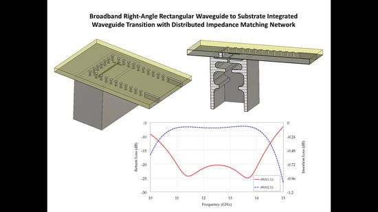
In this paper a novel right-angle RWG-to-SIW transition is presented, which makes use of a distributed impedance matching network, in the form of symmetric E-plane irises. Bandwidth performance depends on the number of matching elements introduced. A prototype is manufactured with stereolithography (SLA) technology and then electroplated. Good agreement between simulated and measured results is observed. Circuit and full-wave simulations are respectively performed with the commercial software NI AWR (AWR Microwave Office 9 by National Instruments) Microwave Office and CST Microwave Studio (CST Microwave Studio 2015 by Dassault Systems).
2. Transition Design
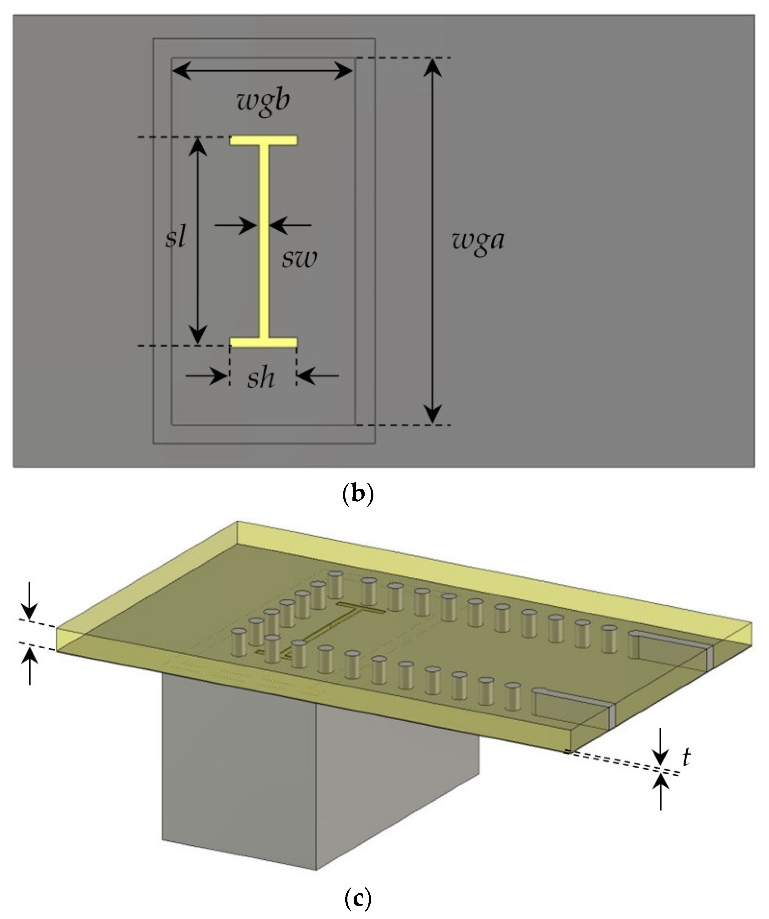
The transition configuration consists of a standard WR75 waveguide connected perpendicularly to a SIW through a H-shaped coupling slot etched in the SIW bottom ground plane, as shown in
Figure 1. The SIW top ground plane is hidden for better clarity.
The characteristic impedance and the propagation constant of this SIW were equal to a dielectric-filled RWG with an equivalent width
ae and the same height, as explained in [
22,
23]. The other edge of the SIW ends with a short circuit at a distance
s, which was kept fixed for reasons to be discussed in the next section. Also, the slot dimensions remained unchanged and were optimized in order to maximize the transmission coefficient to the SIW with no matching elements. The H-shaped slot could be seen as a short double-ridge waveguide section and its cut-off frequency, equal to 9.15 GHz, was low enough to let the electromagnetic field propagate between the two transmission lines. A 2:1 hole pitch-to-diameter ratio was chosen for a reliable manufacturing. To minimize the insertion loss, the adopted substrate was RT5880 by Rogers Corporation, with a dielectric constant
εr = 2.2 and tan
δ = 0.001 measured at 10 GHz. The substrate height was
b = 1.575 mm and the metal thickness was
t = 35 μm, though it was increased to 45 μm in the design to include the effects of the metal hole deposition in a following manufacturing process. The design center frequency was around 12.5 GHz and the simulation bandwidth was between 10 to 15 GHz, which is the typical operating frequency range for a WR75 waveguide. The transition geometrical parameters and simulated scattering parameters are presented in
Table 1 and
Figure 2. The RWG and the SIW are respectively indicated with port indices 1 and 2.
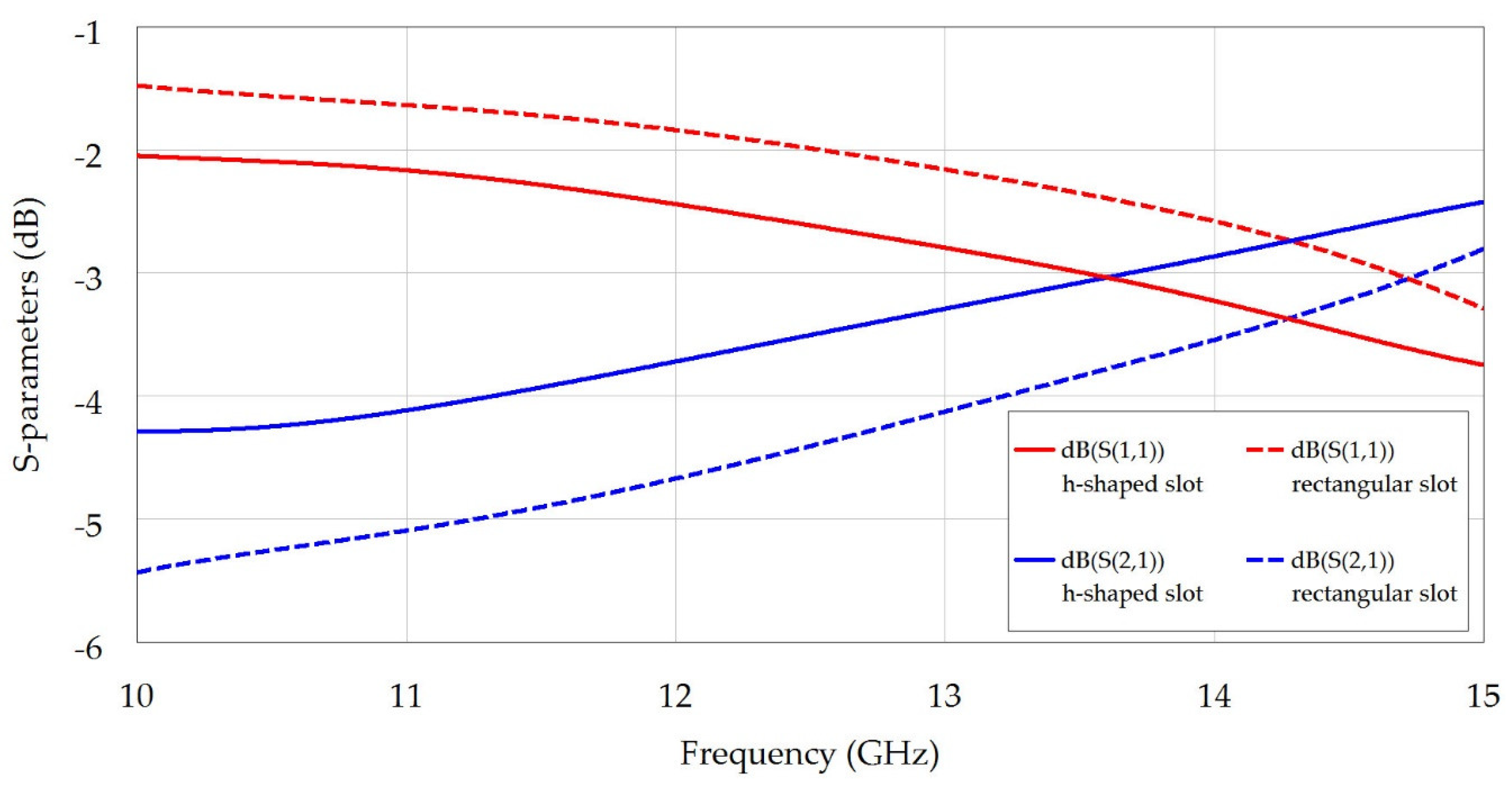
It is evident that, with no matching elements included, such transition exhibits poor return loss performance and cannot be utilized in hybrid feeding networks for large planar array antennas. It is worth mentioning that similar performance would be obtained with any other slot shape, given the fact that the equivalent load connected to the RWG presents a very low impedance, tending towards a short circuit when the substrate thickness becomes very small. Nevertheless, the thinner the slot width
sw, the higher is the transmission coefficient. In addition to that, by adopting an H-shaped slot, the return loss at the RWG port can be further improved. In
Figure 2 the scattering parameters obtained with a standard rectangular slot (
sh =
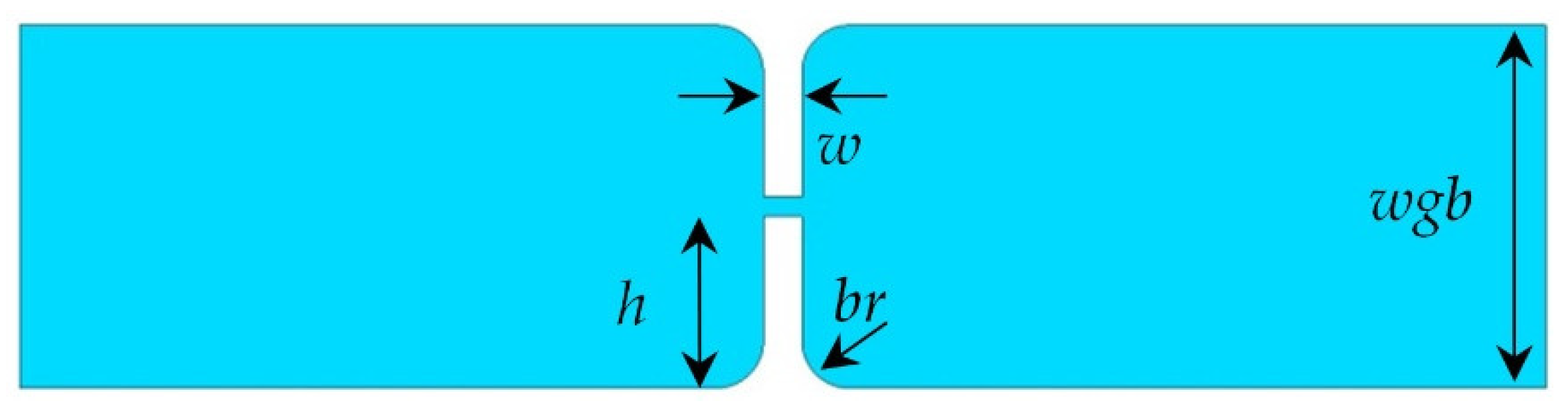
sw, dashed lines) and the optimized H-shaped slot (solid lines) are compared. An improvement of about 1 dB in the return loss can be observed. The transition with the H-shaped slot therefore represents a good starting point for the design of a distributed impedance matching network. The latter can be realized by a number of symmetric irises carved in the RWG E-plane, as depicted in
Figure 3. Each iris is specified by its height
h and its width
w. Without loss of generality, a constant iris width equal to
w = 1 mm was adopted. A blending radius
br = 1.25 mm was considered to ease a fabrication process in the case of CNC (computer numerical control) milling machine manufacturing.
Wideband matching can be achieved with multi-section matching networks, which can be quickly synthesized with the aid of a circuit simulation software. On the other hand, a full-wave simulation software can accurately predict the performance of an electromagnetic structure, at the expense of increased computational cost. Since a complete full-wave design of a matching network with more than one iris would be extremely time-consuming and convergence could not be ensured, the idea was to perform a hybrid synthesis using both simulators. In particular, a proper equivalent circuit associated to the iris geometrical parameters was extracted and then employed in the design of a wideband matching network at a circuit level, and finally the output geometrical parameters were used in the full-wave design. Note that a circuit simulation does not take into account potential higher order modes interactions, thus a final full-wave optimization may be necessary. Anyway, given this first estimate, this process would lead to a very good return loss performance quite rapidly.
It is well known from waveguide theory that a symmetric E-plane iris can be schematized as an equivalent shunt capacitance [
24,
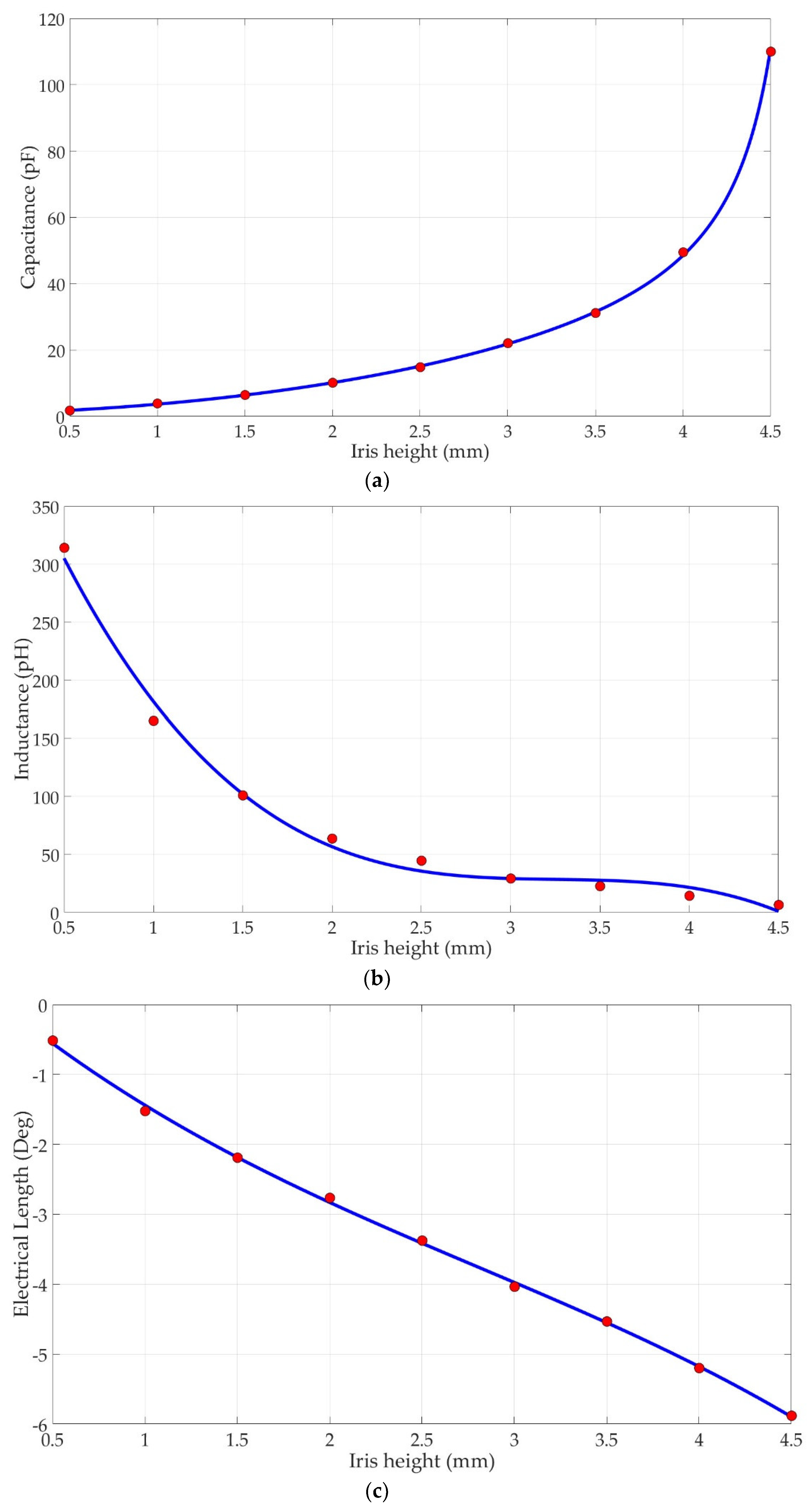
25], but this statement holds true only in a neighborhood of the center frequency. As a consequence, such circuits cannot accurately predict the iris behavior in terms of scattering parameters over the large bandwidth required in many applications and, for this reason, another model must be derived. In this design the iris is to be characterized when its height
h, which is the only varying parameter, is swept from 0.5 mm to 4.5 mm with a step of 0.5 mm. A total of nine scattering matrices are extracted from full-wave simulations and, for each geometrical configuration, it can be verified from circuit simulations that a suitable broadband modeling of the iris can be achieved by introducing a lumped shunt inductance. The equivalent circuit is shown in
Figure 4.
It consists of one capacitance
C and one inductance
L connected so as to form a shunt
LC resonator. In addition to this, two identical transmission lines with normalized impedance
Z0 = 1 and electrical length
θ are introduced to account for second order contributions to the phase of the electric field. For each sampled iris configuration, defined by the parameter
h, an optimization of the three circuit element values
C,
L, and
θ, is to be performed so that the scattering matrix of the equivalent circuit fits the corresponding one from the full-wave simulation over a wide bandwidth. The fitting procedure results are listed in
Table 2.
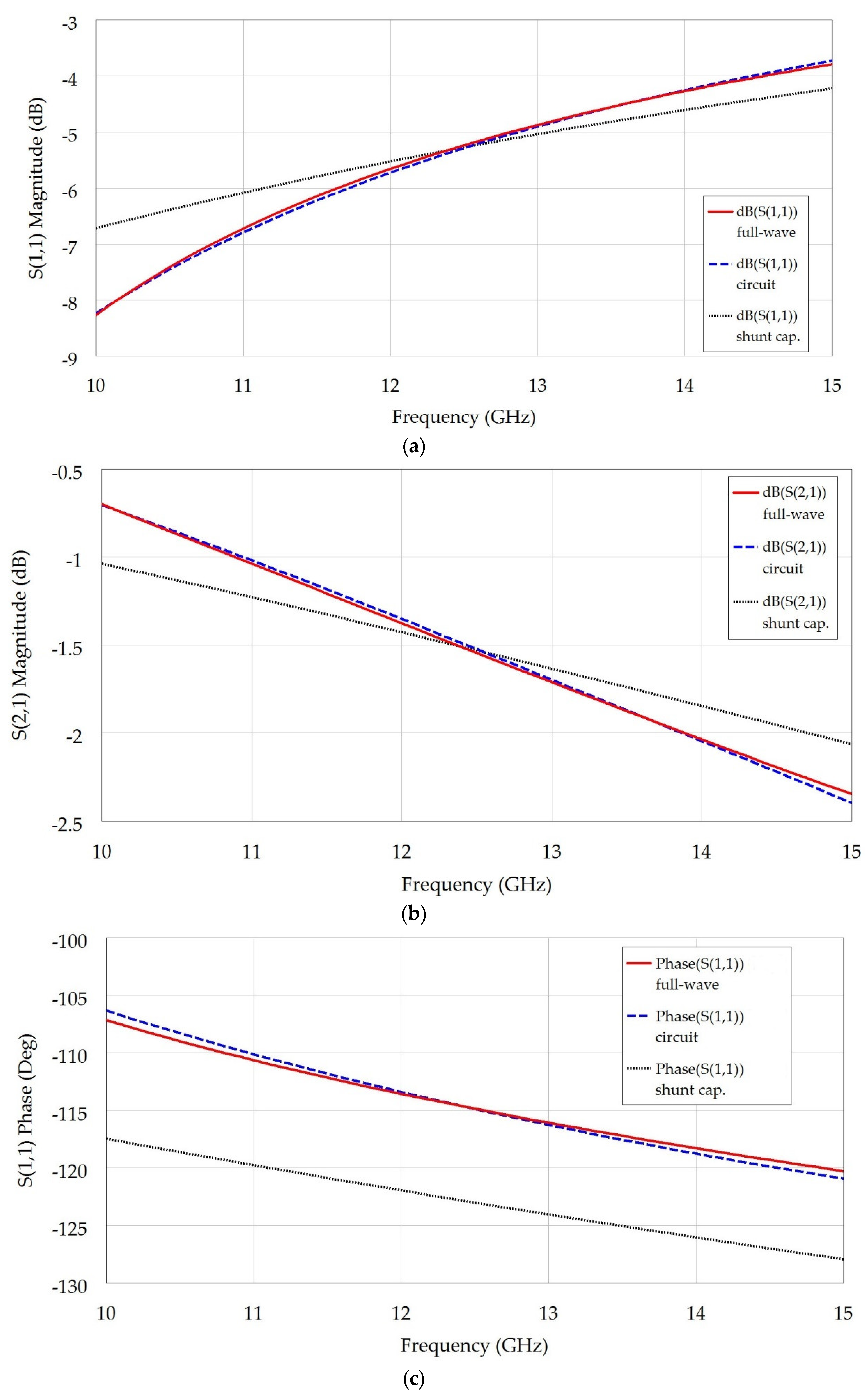
The proposed equivalent circuit performance for a selected iris geometry are reported in
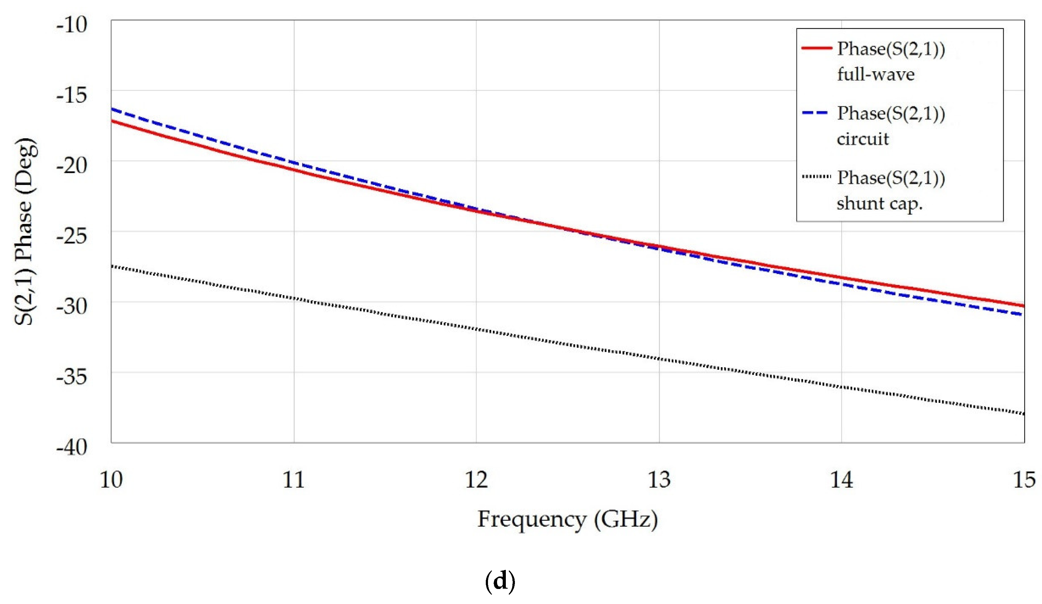
Figure 5, both in magnitude and phase, and compared with the standard shunt capacitance model. A very good agreement was verified on a 40% fractional bandwidth. It is worth mentioning that this wideband fitting cannot be obtained with the standard single-element model.
A least-squares polynomial interpolation of the computed circuit element values was to be performed to have an estimate of the iris scattering matrices for any height value in the above mentioned range. The fitting polynomials grades were selected to be
n = 3 for each parameter as a trade-off between interpolation accuracy and computational cost in the following design stage. Fitting polynomials for
C,
L, and
θ were:
Note that (1) differs from the cubic curves (2) and (3) because of a vertical asymptote given by the geometrical upper limit for the iris height, which completely shorts the waveguide when
h =
wgb/2. Once the interpolation coefficients
ci,
li, and
ti are calculated, Equations (1)–(3) can be easily implemented in any circuit simulation software and scattering matrices with an accuracy close to that of a full-wave simulator can be obtained. The polynomial coefficients and interpolation results are respectively shown in
Table 3 and
Figure 6 for completeness sake.
At this point, the design of a multi-section matching network was straightforward. The subcircuits representing single irises were cascaded and separated by short RWG sections, modeled as transmission lines with normalized impedance
Z0 = 1 and electrical lengths
θi = βLi, where
β is the propagation constant calculated with classical waveguide theory [
24,
25] and
Li is the specific section physical length. A two-section matching network is presented in
Figure 7 as an example: In particular, the circuit representation and physical implementation are illustrated.
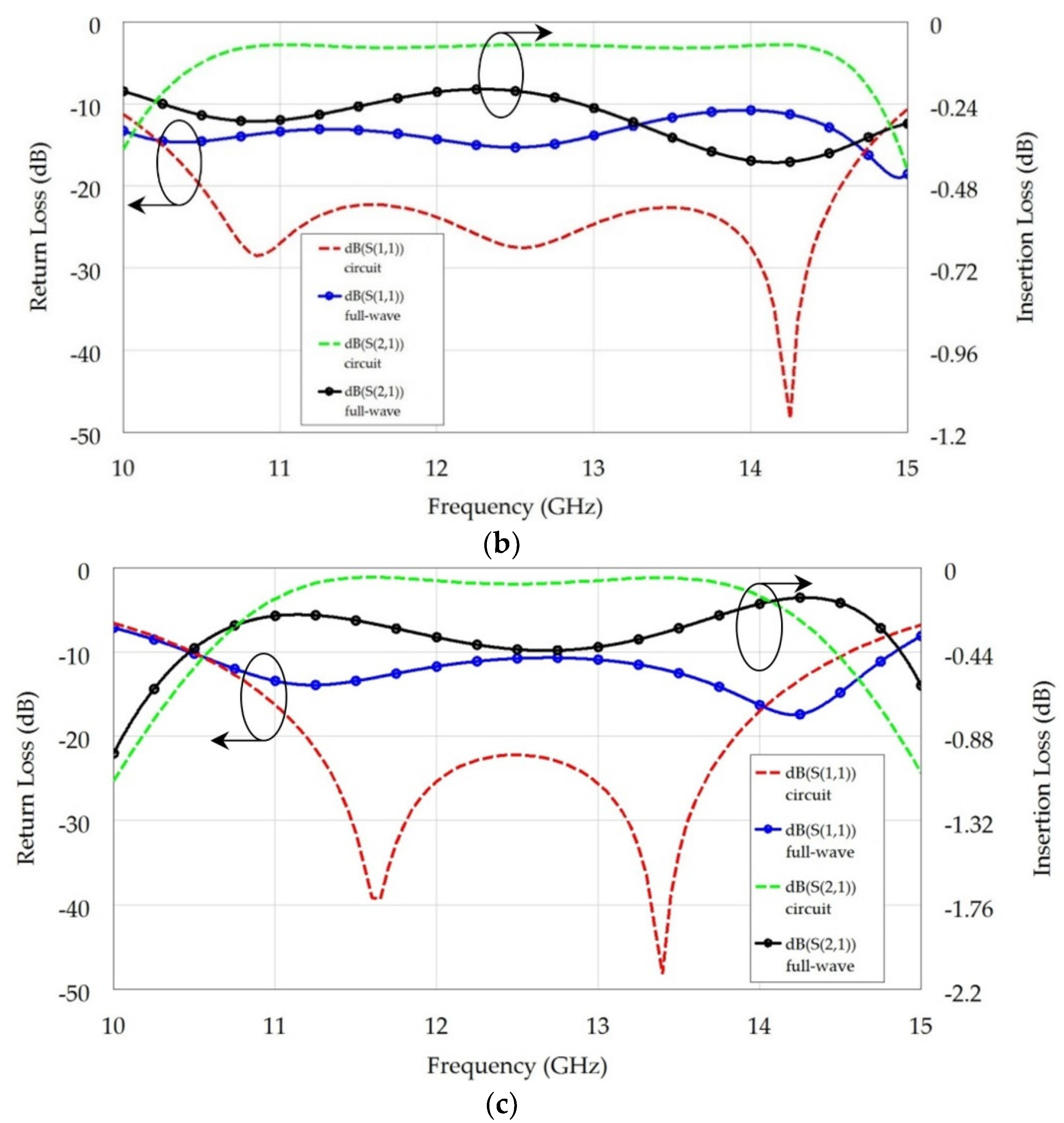
Three matching networks including one, two, and three irises were designed with the circuit simulator to obtain the largest 20-dB return loss bandwidth. Once the irises heights and waveguide sections physical lengths were calculated, corresponding full-wave simulations were carried out to verify the agreement. Geometrical parameters are listed in
Table 4 and a comparison between circuit and full-wave simulated scattering parameters are reported in
Figure 8.
The discrepancy between circuit and full-wave curves is to be imputed to higher order modes that are excited in the waveguide sections between adjacent irises and near the coupling slot and were not taken into account in this simple unimodal circuit simulation. Such modes degrade the return loss levels and, in the third case, a resonance disappears. A final full-wave optimization was therefore necessary, but the computational effort was considerably eased since optimum values were close to the starting one calculated previously. This is the great advantage of the presented method, which resides in the implementation of the model in a circuit simulation software, leading to a quicker matching network design when compared to a pure full-wave solution. Optimized matching networks parameters and simulated scattering parameters are shown in
Table 5 and
Figure 9.
The 20-dB return loss bandwidth improves with an increasing number of irises. Fractional bandwidths of 3.28%, 17.59%, and 24.51% were obtained in the three cases. Insertion loss was better than 0.2 dB and flatter in the frequency ranges corresponding to good input port matching.
A comparison in terms of bandwidth and dimensions between this device and right-angle RWG-to-SIW transitions in referenced works [
12,
13,
14,
15,
16,
17,
18,
19,
20,
21] is presented in
Table 6. All geometrical parameters refer to the SIW. In particular, the SIW height (i.e. the substrate thickness) is defined as fractions of the cut-off wavelength
in the ratio
r. As the substrate thickness decreases, the SIW broad walls get closer to one another. The lower the ratio
r the lower the SIW section input impedance, and as a consequence the harder is to obtain good matching over a wide band. To perform a fair comparison between the various solutions reported in the literature [
12,
13,
14,
15,
16,
17,
18,
19,
20,
21] the bandwidth performance are therefore normalized with the introduction of the merit factor
F =
BW20dB/r. It is worth mentioning that simulated results for standalone transitions are reported, in order to provide a comparison among data not affected by manufacturing errors in the fabricated prototypes.
Though the fractional bandwidth of the present work is not the largest among the list of referenced papers, the high performance of the proposed solution becomes evident when considering also the ratio r and the merit factor F.
3. Transition Manufacturing and Test
The single-iris version was selected for experimental validation because of its higher robustness with respect to manufacturing tolerances. To ease the manufacturing process the RWG was split into two blocks, fabricated with a Form 2 SLA printer by Formlabs and metalized with a two-step process consisting of silver painting followed by electrolytic copper deposition in a copper sulfide solution. Electrical contact between the two manufactured parts was provided by screws. Further details on this SLA additive manufacturing and metallization are discussed in [
26]. This process was adopted in order to minimize time and costs and has exhibited good results for other proof-of-concept prototypes [
27,
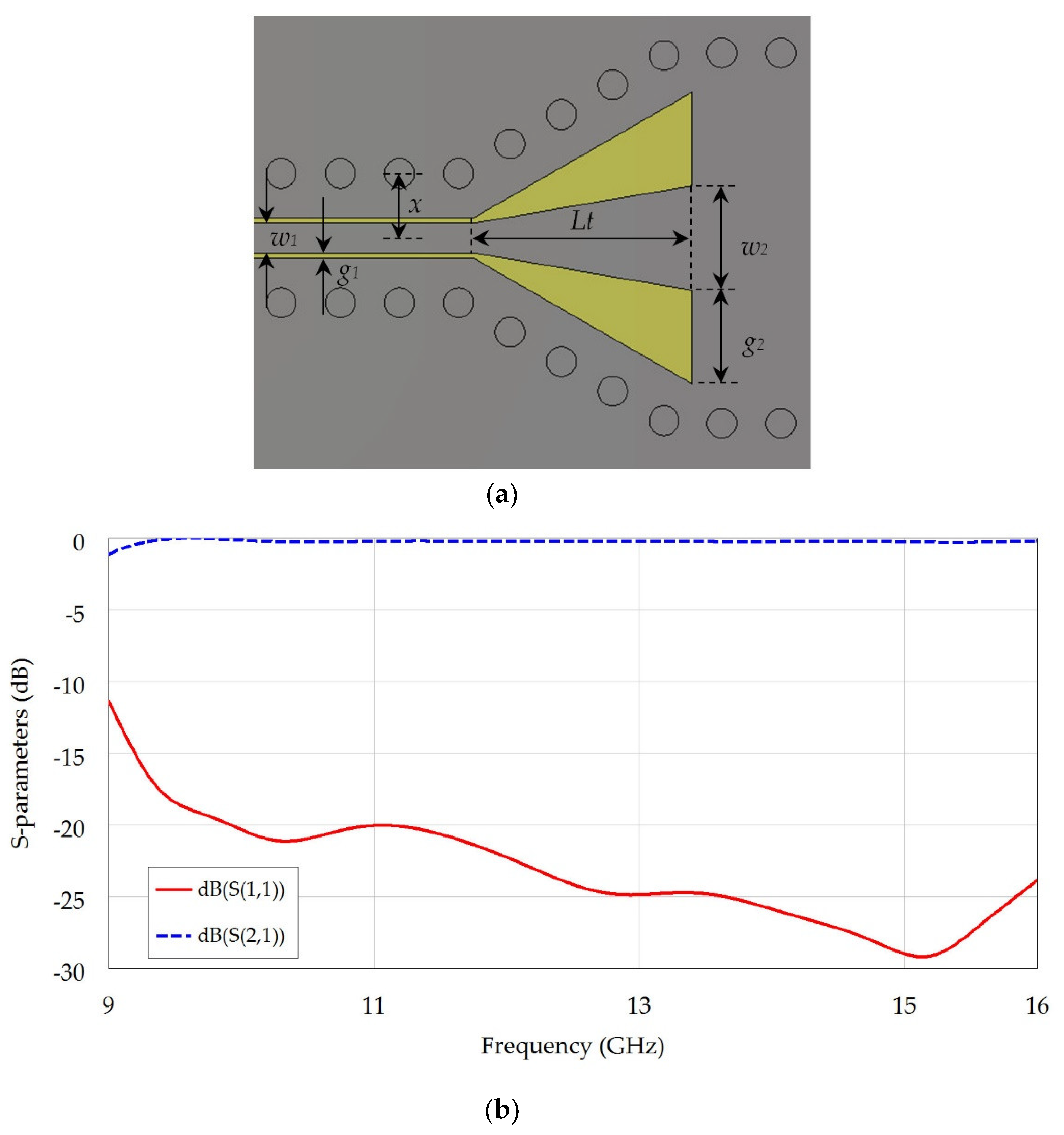
28]. The SIW circuit was manufactured with standard PCB technology and then connected to the RWG, the latter being integrated in a mechanical support structure with mounting screws tightened in six holes drilled in the PCB. A GCPW feeding section for port 2 was preferred over a microstrip line because of a reduced insertion loss due to spurious radiation and a lower influence with the RWG mechanical support. In addition to this, it was easy to integrate a GCPW transmission line with a K-type solder-less connector adopted for the measurements, which is the 2.92-mm jack (female) end-launch connector model 1092-03A-5 by Southwest Microwave. A SIW-to-GCPW transition was designed according to [
29] and included in the following simulations. In particular, a properly dimensioned tapered section converts the frequency-dependent SIW impedance to the GCPW 50-Ω port impedance with a return loss better than 20 dB in the bandwidth of interest. The SIW-to-GCPW transition geometry, simulated performance, and geometrical parameters are respectively reported in
Figure 10 and
Table 7.
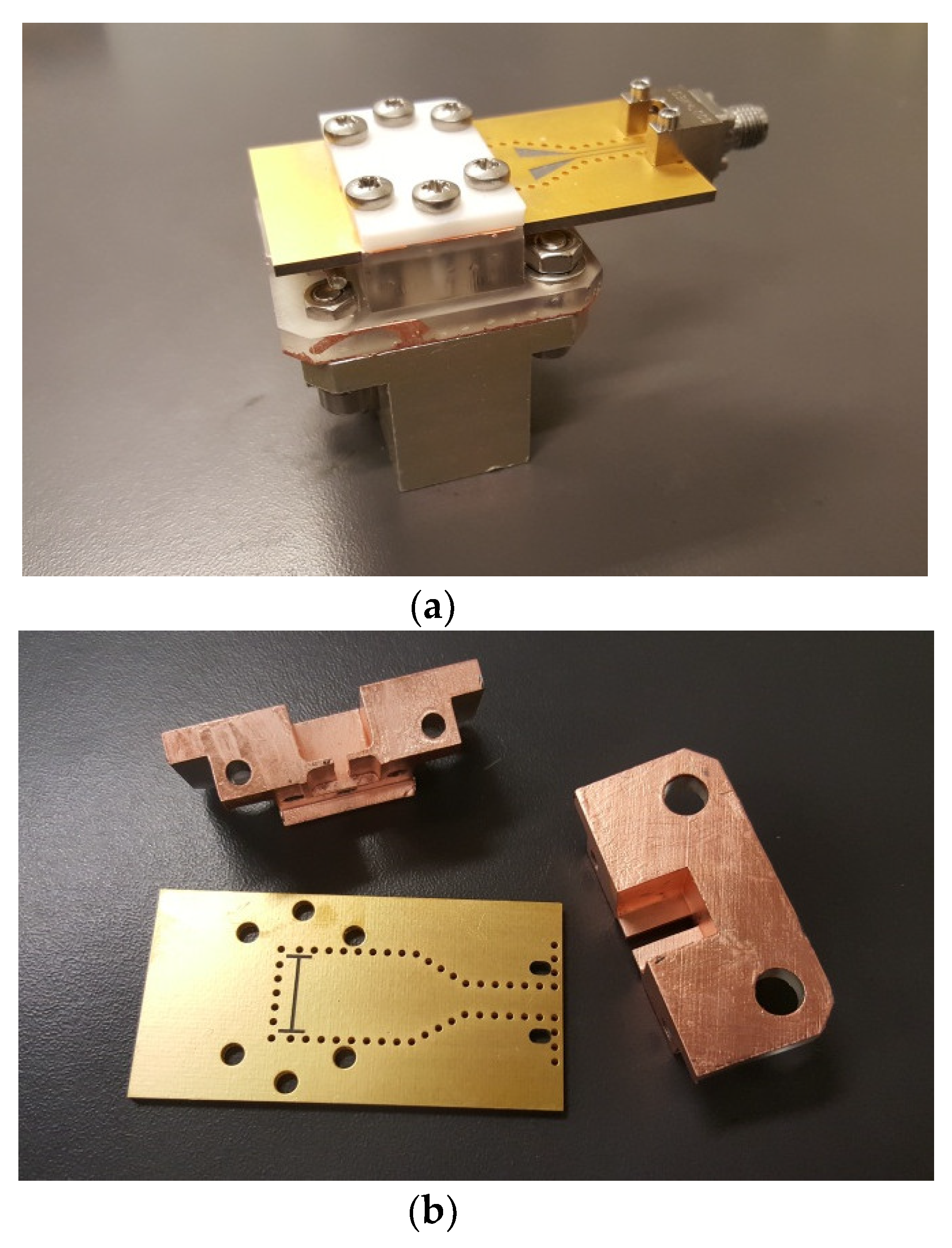
A complete prototype is shown in
Figure 11a after the assembly. In
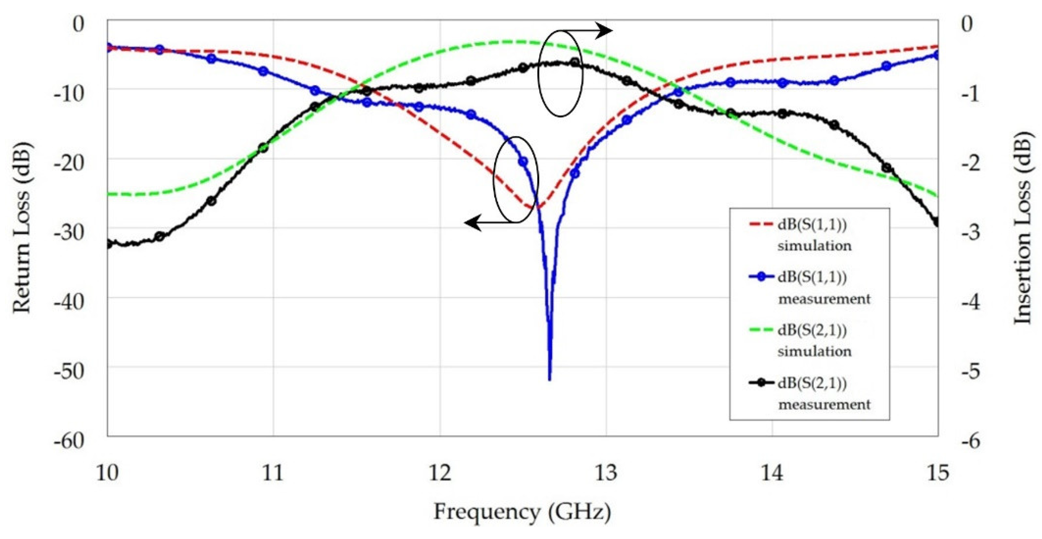
Figure 11b the fabricated RWG is open to visualize the internal details. The prototypes were tested with an Agilent N5230A vector network analyzer using the well-known full two-port short-open-load-through calibration technique. Measured performances are reported in
Figure 12 and compared to simulated results. Physical properties of copper conductivity and material roughness were taken into account in the simulation. In particular, an estimated metallic roughness on the order of 5 μm contributed to deteriorate copper conductivity. A de-embedding procedure was also applied to the measured results in order to remove the effects of the coaxial connector as in [
30], relying on the datasheet and measured data provided by the manufacturer. The estimated insertion loss for the connector is approximately 0.4 dB at 10 GHz and 0.5 dB at 15 GHz.
Measured results showed a good agreement with simulations, though a small frequency shift in the return loss and a slightly larger insertion loss were observed. Discrepancies in the return loss can be explained by a 0.1-mm fabrication tolerance associated with the SLA manufacturing, misalignment errors and plastic deformation in the assembling. The increased insertion loss was due to a poor electric contact between the PCB and 3D-printed RWG section. The same device, manufactured in aluminum with a CNC milling machine and assembled with standard industrial processes, would have improved the agreement between simulated and measured results, at the expense of higher costs. Nevertheless, measured curves are indicative of good performance for the mentioned fast in-house fabrication process.


