
A Review on Progress, Challenges, and Prospects of Material Jetting of Copper and Tungsten
 , , ,
, , ,  , and
, and
Abstract
:1. Introduction

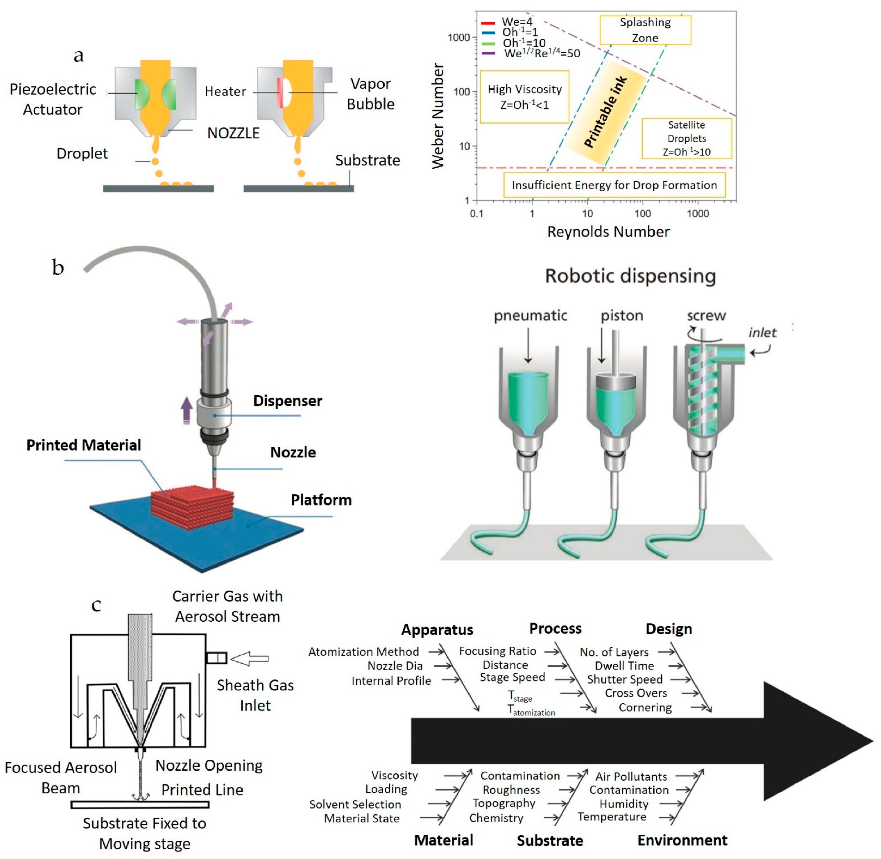
2. Material Jetting Techniques
2.1. Inkjet Printing (IJP)
2.2. Direct Ink Writing (DIW)
2.3. Aerosol Jet Printing (AJP)
2.4. Applications of IJP, DIW, and AJP
3. Cu and W Printing
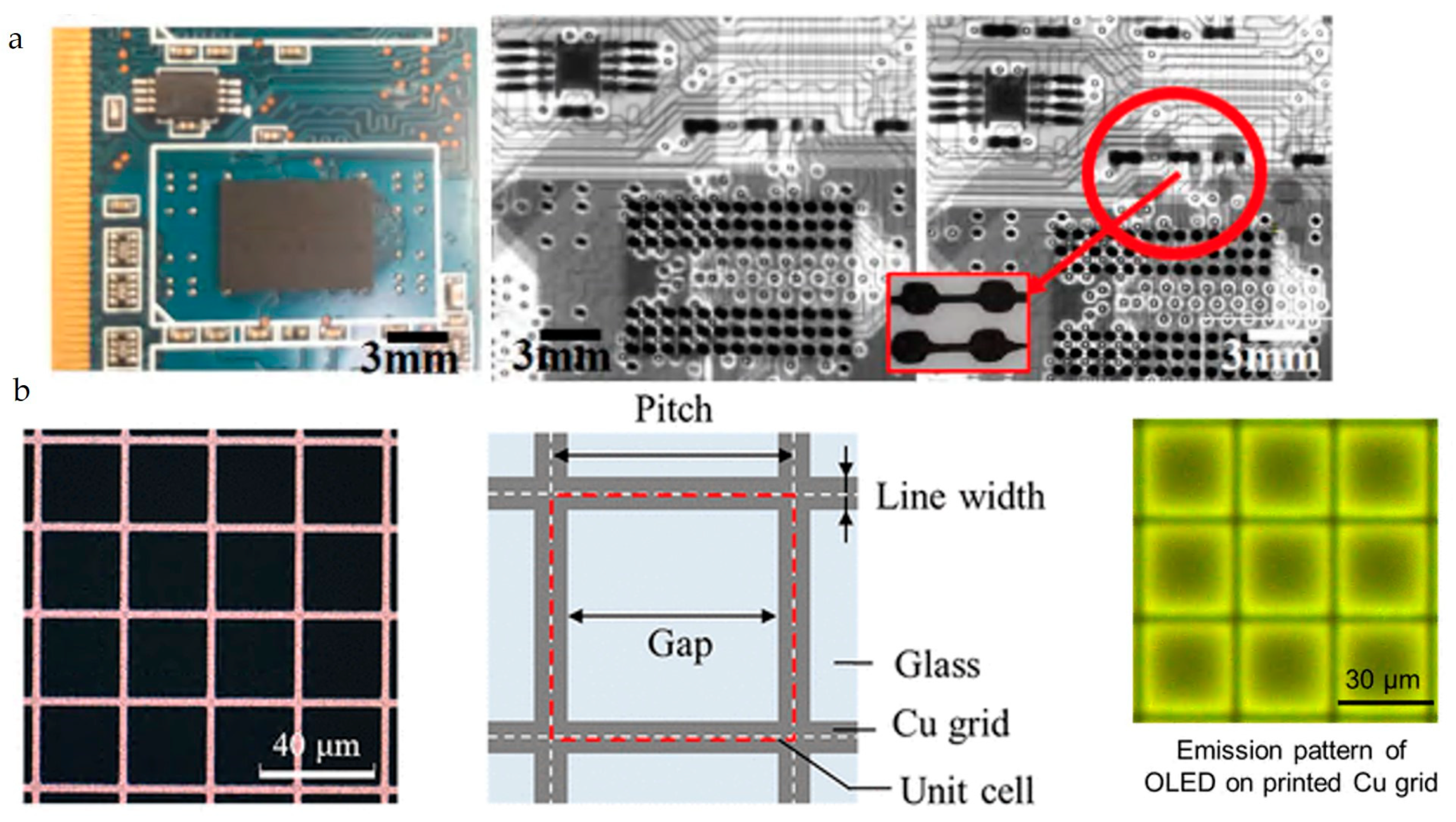
3.1. Current Reported Applications of Printed Cu and W

| Material | Ink Type | Printing Method | Post-Processing Technique | Optimum Resistivity (Conductivity) | Application | Reference |
|---|---|---|---|---|---|---|
| Cu | NPs | IJP | Laser sintering | 0.5 µΩ □−1 (3.6 kS·cm−1) | Current collecting grids for photovoltaics | [162] |
| Cu | Core-shell NPS | IJP | Conventional sintering | 11 µΩ·cm | Conductive patterns for electronics | [168] |
| Cu | NPs | IJP | Conventional sintering | 13.5 µΩ·cm | Conductive patterns | [169] |
| Cu | Precursor | IJP | Conventional sintering | 9.5 µΩ·cm | Conductive patterns | [170] |
| Cu | Precursor | IJP | Conventional sintering | 10.5 µΩ·cm | Conductive patterns | [171] |
| Cu | Precursor | IJP | Conventional sintering | (15 kS·cm−1) | Conductive patterns | [172] |
| Cu | Precursor | IJP | sintering in formic acid | 2.3 µΩ·cm | Conductive patterns | [173] |
| Cu | Precursor | IJP | Conventional sintering | - | Binding material in binder jetting, an additive manufacturing technology, to produce copper structures | [174] |
| Cu | NPs | IJP | Conventional sintering | - | Binding material in binder jetting, an additive manufacturing technology, to produce copper structures | [175] |
| Cu | NPs | IJP | Photonic sintering | <2.5 µΩ·cm | Circuits | [164] |
| Cu | NPs | AJP | CW laser sintering | 18 µΩ·cm | To repair the PCB board | [163] |
| Cu–Mn | Microparticles | DIW | Conventional sintering | - | Hierarchical porous alloy could be used in catalysis, sensors, electrodes, and actuators applications | [176] |
| Cu | NPs | DIW | Conventional sintering | 1 × 10⁴ µΩ □−1 | Interconnects | [165] |
| Cu | Microparticles | DIW | Conventional sintering | (2.8 kS·cm−1) | Support structures for steel | [177] |
| Cu–Ni | NPs | AJP | Conventional sintering | 1.0 × 10⁶ µΩ □−1 | Resistor for power applications | [166] |
| Cu and alloys | NPs | AJP | Conventional sintering | - | Resistance temperature sensors | [167] |
| Cu | Shear thinning Cu microparticle ink | DIW | Conventional sintering | - | 3D porous scaffold for Li-ion batteries | [56] |
| Cu | NPs | AJP | Conventional and photo sintering | <15.0 µΩ·cm | Conductive patterns | [178] |
| Cu and Cu-Graphene | NPs | AJP | Conventional sintering | (1.5 kS·cm−1) | Conductive patterns | [179] |
| W | Precursor | AJP | Conventional sintering | - | Porous nanostructured coating for enhancing solar absorption | [159] |
| W | NPs | DIW | Conventional sintering | - | Could be used for ultrahigh-voltage electric contacts | [180] |
| W | NPs | DIW | Conventional sintering | - | Could be used for heat exchangers | [181] |
3.2. Commercial Cu and W Inks
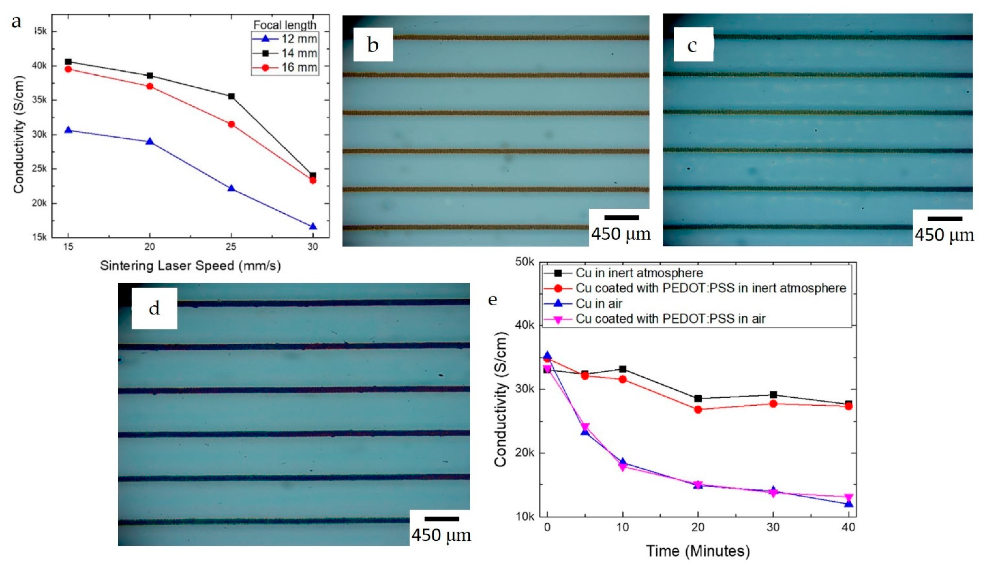
3.3. Challenges and Progress of Printing Cu
3.3.1. IJP of Cu
3.3.2. DIW of Cu
3.3.3. AJP of Cu
3.4. Challenges and Progress of Printing W
3.4.1. IJP of W
3.4.2. DIW of W
3.4.3. AJP of W
4. Integration of SBAM Material Jetting within Powder Bed-Based MAM
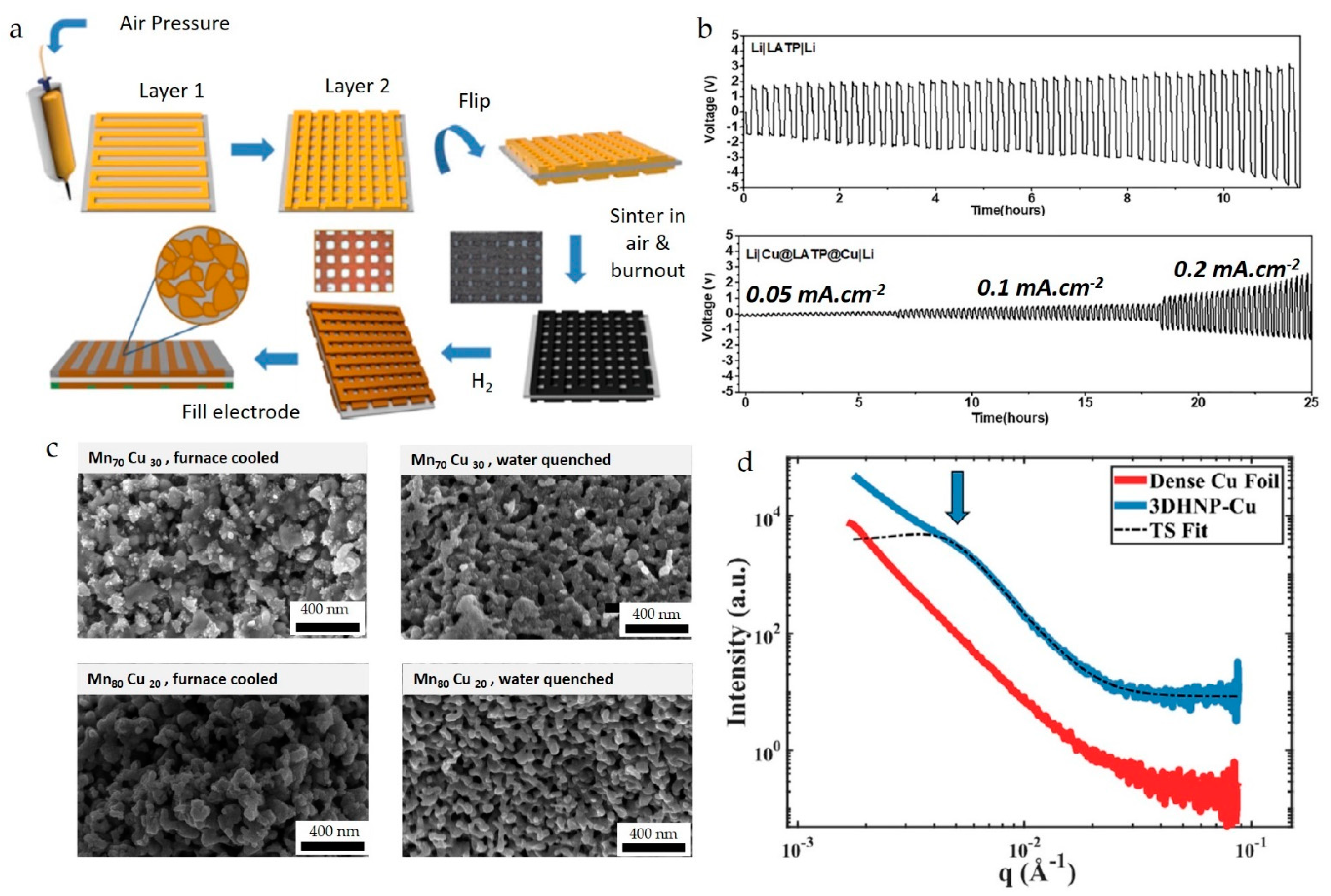
4.1. Binder Jetting Additive Manufacturing (BJAM)
4.2. Hybrid Laser Powder Bed Fusion (LPBF)
5. Factors Influencing Large-Scale Fabrication
5.1. Scaling Up of Synthesis of NPs and Precursor for Ink
5.2. Post-Processing after Printing Ink
5.3. SBAM within Powder Bed-Based MAM
5.3.1. BJAM
5.3.2. Hybrid LPBF
6. Summary and Outlook
- The oxidation of Cu NPs and the printed track has been addressed through various techniques. The techniques include core-shell NPs, laser sintering, protective coating layers, and the development of new precursor MOD inks that do not require reducing agents to convert to Cu. Factors such as solvent evaporation, cooling rates, and ink composition have been reported to control the morphology and microstructure of printed parts;
- Photothermal conversion of solution-printed volatile precursors has been employed to address the challenges related to the unavailability of precursor chemistry. Additionally, wetting agents have been used to improve the sintering of W-based composites;
- The challenges associated with large-scale fabrication include synthesizing NPs or precursors for ink formulations and performing post-treatment on the printed ink. Both microfluidic channels and mechanochemical syntheses have been identified as viable approaches for scaling up ink production;
- NPs and precursor inks have been utilized to produce three-dimensional parts using BJAM, paving the way for selective doping;
- Various metal matrix composites have been fabricated using hybrid LPBF integrated with material jetting techniques;
- This hybrid LPBF method is expected to reduce manufacturing time for producing metal matrix composites by eliminating the need for mixing two different powders via ball-milling;
- This hybrid LPBF method can create functional alloys with selectively tailored thermal properties through the selective doping of Cu and W.
- The development of Cu–Ni, Cu–Ag, and Cu–Cu formate core-shell NPs inks has been discussed in the article. However, no reported works on Cu–W or alloying Cu–W NPs with other metal NPs exist. The synthesis of such multi-alloyed NPs is possible through controlled microfluidic synthesis. Investigating the printing and sintering of these films could be beneficial, as adding W to Cu improves its mechanical properties and high-temperature resistance, while adding Cu to W enhances its electrical and thermal conductivities [26];
- Recent work by Bernasconi et al. [226] demonstrates that highly viscous fluids can be jetted using drop-on-demand piezoelectric printheads. These types of printheads could address the concern of low solid loading (percent of NPs or precursors inside the carrier solvent) in inks used in inkjet printing mechanisms for hybrid LPBF-Inkjet systems, particularly when a significant amount of second-phase material is required;
- Additionally, investigating new stand-alone W precursors or combining them with Cu MOD precursors could increase the options for selecting and formulating inks;
- Recently, grain refinement and strengthening of the Cu matrix with nanoscale W particles have been reported [227]. There are existing works on synthesizing W NPs (Table 3). Formulating inks and doping these into the powder bed could enable the fabrication of interesting three-dimensional structures for applications such as heat exchangers.
Author Contributions
Funding
Data Availability Statement
Conflicts of Interest
References
- Liu, L.; Li, M.; Lyu, J.; Zhao, T.; Li, T. Facile and Green Preparation of Three-Dimensionally Nanoporous Copper Films by Low-Current Electrical Field-Induced Assembly of Copper Nanoparticles for Lithium-Ion Battery Applications. J. Mater. Eng. Perform. 2018, 27, 4680–4692. [Google Scholar] [CrossRef]
- Deore, B.; Paquet, C.; Kell, A.J.; Lacelle, T.; Liu, X.; Mozenson, O.; Lopinski, G.; Brzezina, G.; Guo, C.; Lafrenière, S.; et al. Formulation of Screen-Printable Cu Molecular Ink for Conductive/Flexible/Solderable Cu Traces. ACS Appl. Mater. Interfaces 2019, 11, 38880–38894. [Google Scholar] [CrossRef] [PubMed]
- Hlina, J.; Reboun, J.; Simonovsky, M.; Syrovy, T.; Janda, M.; Hamacek, A. Study of New Nitrogen-Fireable Copper-Nickel Thick Film Paste Formulation Compatible with Thick Printed Copper. Materials 2022, 15, 1372. [Google Scholar] [CrossRef] [PubMed]
- Hlina, J.; Reboun, J.; Johan, J.; Simonovsky, M.; Hamacek, A. Reliability of printed power resistor with thick-film copper terminals. Microelectron. Eng. 2019, 216, 111095. [Google Scholar] [CrossRef]
- Li, W.; Li, L.; Li, F.; Kawakami, K.; Sun, Q.; Nakayama, T.; Liu, X.; Kanehara, M.; Zhang, J.; Minari, T. Self-Organizing, Environmentally Stable, and Low-Cost Copper-Nickel Complex Inks for Printed Flexible Electronics. ACS Appl. Mater. Interfaces 2022, 14, 8146–8156. [Google Scholar] [CrossRef]
- Wang, R.; Liu, H.; Wang, X.; Li, X.; Gu, X.; Zheng, Z. Plasmon-enhanced furfural hydrogenation catalyzed by stable carbon-coated copper nanoparticles driven from metal-organic frameworks. Catal. Sci. Technol. 2020, 10, 6483–6494. [Google Scholar] [CrossRef]
- Gamarra, D.; Munuera, G.; Hungrı, A.B.; Ferna, M.; Martı, A. Structure—Activity Relationship in Nanostructured Copper—Ceria-Based Preferential CO Oxidation Catalysts. J. Phys. Chem. C 2007, 111, 11026–11038. [Google Scholar] [CrossRef]
- Ren, L.; Tong, L.; Yi, X.; Zhou, W.; Wang, D.; Liu, L.; Ye, J. Ultrathin graphene encapsulated Cu nanoparticles: A highly stable and efficient catalyst for photocatalytic H2 evolution and degradation of isopropanol. Chem. Eng. J. 2020, 390, 124558. [Google Scholar] [CrossRef]
- Nam, G.; Park, J.; Choi, M.; Oh, P.; Park, S.; Kim, M.G.; Park, N.; Cho, J.; Lee, J.-S. Carbon-Coated Core–Shell Fe–Cu Nanoparticles as Highly Active and Durable Electrocatalysts for a Zn–Air Batte. ACS Nano 2015, 9, 6493–6501. [Google Scholar] [CrossRef]
- Guan, Y.; Li, N.; Li, Y.; Sun, L.; Gao, Y.; Zhang, Q.; He, C.; Liu, J.; Ren, X. Two dimensional ZIF-derived ultra-thin Cu-N/C nanosheets as high performance oxygen reduction electrocatalysts for high-performance Zn-air batteries. Nanoscale 2020, 12, 14259–14266. [Google Scholar] [CrossRef]
- Kang, W.J.; Feng, Y.; Li, Z.; Yang, W.Q.; Cheng, C.Q.; Shi, Z.Z.; Yin, P.F.; Shen, G.R.; Yang, J.; Dong, C.K.; et al. Strain-Activated Copper Catalyst for pH-Universal Hydrogen Evolution Reaction. Adv. Funct. Mater. 2022, 32, 2112367. [Google Scholar] [CrossRef]
- Wang, Y.; Raciti, D.; Wang, C. High-Flux CO Reduction Enabled by Three-Dimensional Nanostructured Copper Electrodes. ACS Catal. 2018, 8, 5657–5663. [Google Scholar] [CrossRef]
- Li, L.-J.; Wang, X.-Q.; Li, J.-W.; Jia, Q.-Y.; Yang, H.-J.; Bo, Y.-Q.; Liu, Z.-Q.; Zhang, P.-F.; Kong, L.-X. Sensitivity-enhanced fiber-optic surface plasmon resonance sensor utilizing Cu/WS2/PAAG composite film for pH measurement. Optik 2022, 260, 169075. [Google Scholar] [CrossRef]
- Hassan, H.H.; Badr, I.H.A.; Abdel-Fatah, H.T.M.; Elfeky, E.M.S.; Abdel-Aziz, A.M. Low cost chemical oxygen demand sensor based on electrodeposited nano-copper film. Arab. J. Chem. 2018, 11, 171–180. [Google Scholar] [CrossRef] [Green Version]
- Thakur, B.; Bernalte, E.; Smith, J.P.; Foster, C.W.; Linton, P.E.; Sawant, S.N.; Banks, C.E. Utilising copper screen-printed electrodes (CuSPE) for the electroanalytical sensing of sulfide. Analyst 2016, 141, 1233–1238. [Google Scholar] [CrossRef] [Green Version]
- Li, C.; Wang, Z.; Wang, P.I.; Peles, Y.; Koratkar, N.; Peterson, G.P. Nanostructured copper interfaces for enhanced boiling. Small 2008, 4, 1084–1088. [Google Scholar] [CrossRef]
- Shi, Y.; Wang, Z.; Gao, H.; Niu, J.; Ma, W.; Qin, J.; Peng, Z.; Zhang, Z. A self-supported, three-dimensional porous copper film as a current collector for advanced lithium metal batteries. J. Mater. Chem. A 2019, 7, 1092–1098. [Google Scholar] [CrossRef]
- Chen, W.J.; Lin, Y.C.; Kumar, G.; Xie, S.Y.; Chen, F.C. Polymer-capped copper nanoparticles trigger plasmonic field for improving performance of perovskite solar cells. Synth. Met. 2021, 273, 116675. [Google Scholar] [CrossRef]
- Shen, P.; Liu, Y.; Long, Y.; Shen, L.; Kang, B. High-Performance Polymer Solar Cells Enabled by Copper Nanoparticles-Induced Plasmon Resonance Enhancement. J. Phys. Chem. C 2016, 120, 8900–8906. [Google Scholar] [CrossRef]
- Tang, M.; Sun, B.; Zhou, D.; Gu, Z.; Chen, K.; Guo, J.; Feng, L.; Zhou, Y. Broad-band plasmonic Cu-Au bimetallic nanoparticles for organic bulk heterojunction solar cells. Org. Electron. 2016, 38, 213–221. [Google Scholar] [CrossRef]
- Chang, W.C.; Weng, L.W.; Chuang, C.K.; Liang, J.X.; Yang, T.N.; Ma, W.Y. The preparation of antioxidant copper paste and its application to silicon solar cells. J. Nanosci. Nanotechnol. 2016, 16, 9125–9131. [Google Scholar] [CrossRef]
- Liu, Z.; Lee, S.Y.; Lee, E.C. Copper nanoparticle incorporated plasmonic organic bulk-heterojunction solar cells. Appl. Phys. Lett. 2014, 105, 223306. [Google Scholar] [CrossRef]
- Wang, D.D.; Ge, C.W.; Wu, G.A.; Li, Z.P.; Wang, J.Z.; Zhang, T.F.; Yu, Y.Q.; Luo, L.B. A sensitive red light nano-photodetector propelled by plasmonic copper nanoparticles. J. Mater. Chem. C 2017, 5, 1328–1335. [Google Scholar] [CrossRef]
- Wei, C.; Liu, L.; Gu, Y.; Huang, Y.; Chen, Q.; Li, Z.; Li, L. Multi-material additive-manufacturing of tungsten—Copper alloy bimetallic structure with a stainless-steel interlayer and associated bonding mechanisms. Addit. Manuf. 2022, 50, 102574. [Google Scholar] [CrossRef]
- Rehman, T.U.; Ali, H.M.; Saieed, A.; Pao, W.; Ali, M. Copper foam/PCMs based heat sinks: An experimental study for electronic cooling systems. Int. J. Heat Mass Transf. 2018, 127, 381–393. [Google Scholar] [CrossRef]
- Wang, Y.; Zhuo, L.; Yin, E. Progress, challenges and potentials/trends of tungsten-copper (W Cu) composites/pseudo-alloys: Fabrication, regulation and application. Int. J. Refract. Met. Hard Mater. 2021, 100, 105648. [Google Scholar] [CrossRef]
- Lassner, E.; Schubert, W.-D. Tungsten: Properties, Chemistry, Technology of the Elements, Alloys, and Chemical Compounds; Springer Science & Business Media: New York, NY, USA, 1999; ISBN 0306450534. [Google Scholar]
- Kotlarski, G.; Valkov, S.; Andreeva, A.; Mateev, V.; Marinova, I.; Petrov, P. Electrical contact resistance of tungsten coatings deposited on Cu and Al conductors. J. Phys. Conf. Ser. 2021, 1859, 012063. [Google Scholar] [CrossRef]
- Lee, Y.H.; Kim, D.H.; Choi, C.H.; Jang, Y.T.; Ju, B.K. Growth and electrical properties of multidimensional tungsten nano-buliding blocks. Appl. Phys. Lett. 2004, 85, 5977–5979. [Google Scholar] [CrossRef]
- Hou, G.; Wang, Z.; Xu, J.; Chen, K. Tungsten-Coated Silicon Nanopillars as Ultra-Broadband and Thermally Robust Solar Harvesting Materials. ACS Appl. Nano Mater. 2020, 3, 2430–2437. [Google Scholar] [CrossRef]
- Ungaro, C.; Gray, S.K.; Gupta, M.C. Black tungsten for solar power generation. Appl. Phys. Lett. 2013, 103, 4–7. [Google Scholar] [CrossRef]
- Rephaeli, E.; Fan, S. Tungsten black absorber for solar light with wide angular operation range. Appl. Phys. Lett. 2008, 92, 211107. [Google Scholar] [CrossRef]
- Elezovic, N.R.; Zabinski, P.; Ercius, P.; Wytrwal, M.; Radmilovic, V.R.; Lačnjevac, U.; Krstajic, N.V. High surface area Pd nanocatalyst on core-shell tungsten based support as a beneficial catalyst for low temperature fuel cells application. Electrochim. Acta 2017, 247, 674–684. [Google Scholar] [CrossRef] [Green Version]
- Zheng, M.Y.; Wang, A.Q.; Ji, N.; Pang, J.F.; Wang, X.D.; Zhang, T. Transition metal-tungsten bimetallic catalysts for the conversion of cellulose into ethylene glycol. ChemSusChem 2010, 3, 63–66. [Google Scholar] [CrossRef] [PubMed]
- Xiao, Z.Q.; Mao, J.W.; Ji, J.B.; Sha, R.Y.; Fan, Y.; Xing, C. Preparation of nano-scale nickel-tungsten catalysts by pH value control and application in hydrogenolysis of cellulose to polyols. Ranliao Huaxue Xuebao J. Fuel Chem. Technol. 2017, 45, 641–650. [Google Scholar] [CrossRef]
- Xiong, B.; Zhao, W.; Tian, H.; Huang, W.; Chen, L.; Shi, J. Nickel-Tungsten Nano-Alloying for High-Performance hydrogen Electro-Catalytic oxidation. Chem. Eng. J. 2022, 432, 134189. [Google Scholar] [CrossRef]
- Smid, I.; Akiba, M.; Vieider, G.; Plöchl, L. Development of tungsten armor and bonding to copper for plasma-interactive components. J. Nucl. Mater. 1998, 258–263, 160–172. [Google Scholar] [CrossRef]
- Cizek, J.; Vilemova, M.; Lukac, F.; Koller, M.; Kondas, J.; Singh, R. Cold sprayed tungsten armor for tokamak first wall. Coatings 2019, 9, 836. [Google Scholar] [CrossRef] [Green Version]
- Kim, H.; Lee, H.J.; Jang, C. Thermal performance of multilayer PVD tungsten coating for the first wall application in nuclear fusion devices. Fusion Sci. Technol. 2015, 68, 378–382. [Google Scholar] [CrossRef]
- Kundrat, V.; Vykoukal, V.; Moravec, Z.; Simonikova, L.; Novotny, K.; Pinkas, J. Preparation of polycrystalline tungsten nanofibers by needleless electrospinning. J. Alloys Compd. 2022, 900, 163542. [Google Scholar] [CrossRef]
- Takamura, S.; Ohno, N.; Nishijima, D.; Kajita, S. Formation of Nanostructured Tungsten with Arborescent Shape due to Helium Plasma Irradiation. Plasma Fusion Res. 2006, 1, 051. [Google Scholar] [CrossRef] [Green Version]
- Steinhögl, W.; Steinlesberger, G.; Perrin, M.; Scheinbacher, G.; Schindler, G.; Traving, M.; Engelhardt, M. Tungsten interconnects in the nano-scale regime. Microelectron. Eng. 2005, 82, 266–272. [Google Scholar] [CrossRef]
- Calabretta, M.; Sitta, A.; Oliveri, S.M.; Sequenzia, G. An experimental-numeric approach to manufacture semiconductor wafer using thick copper front metallization. Int. J. Interact. Des. Manuf. 2021, 15, 117–119. [Google Scholar] [CrossRef]
- Ayoub, B.; Moreau, S.; Lhostis, S.; Frémont, H.; Mermoz, S.; Souchier, E.; Deloffre, E.; Escoubas, S.; Cornelius, T.W.; Thomas, O. In-situ characterization of thermomechanical behavior of copper nano-interconnect for 3D integration. Microelectron. Eng. 2022, 261, 111809. [Google Scholar] [CrossRef]
- Jia, J.; Bai, S.; Xiong, D.; Xiao, J.; Yan, T. Enhanced thermal conductivity in diamond/copper composites with tungsten coatings on diamond particles prepared by magnetron sputtering method. Mater. Chem. Phys. 2020, 252, 123422. [Google Scholar] [CrossRef]
- Tan, Z.; Li, Z.; Fan, G.; Guo, Q.; Kai, X.; Ji, G.; Zhang, L.; Zhang, D. Enhanced thermal conductivity in diamond/aluminum composites with a tungsten interface nanolayer. Mater. Des. 2013, 47, 160–166. [Google Scholar] [CrossRef]
- Wang, X.; Su, Y.; Wang, X.; Liu, K.; Zhang, L.; Ouyang, Q.; Zhang, D. Fabrication, mechanical and thermal properties of tungsten-copper coated graphite flakes reinforced copper matrix composites. Mater. Des. 2022, 216, 110526. [Google Scholar] [CrossRef]
- Lee, K.; Doddapaneni, V.V.K.; Mirzababaei, S.; Pasebani, S.; Chang, C.; Paul, B.K. Synthesis of a 316L stainless steel-copper composite by laser melting. Addit. Manuf. Lett. 2022, 3, 100058. [Google Scholar] [CrossRef]
- Ugarteche, C.V.; Furlan, K.P.; Pereira, R.d.V.; Trindade, G.; Binder, R.; Binder, C.; Klein, A.N. Effect of Microstructure on the Thermal Properties of Sintered Iron-copper Composites. Mater. Res. 2015, 18, 1176–1182. [Google Scholar] [CrossRef] [Green Version]
- Mirzababaei, S.; Doddapaneni, V.V.K.; Lee, K.; Paul, G.E.; Pirgazi, H.; Tan, K.-S.; Ertorer, O.; Chang, C.; Paul, B.K.; Pasebani, S. Remarkable enhancement in thermal conductivity of stainless-steel leveraging metal composite via laser powder bed fusion: 316L-Cu composite. Addit. Manuf. 2023, 70, 103576. [Google Scholar] [CrossRef]
- Singh, M.; Mulla, M.Y.; Santacroce, M.V.; Magliulo, M.; Di Franco, C.; Manoli, K.; Altamura, D.; Giannini, C.; Cioffi, N.; Palazzo, G.; et al. Effect of the gate metal work function on water-gated ZnO thin-film transistor performance. J. Phys. D Appl. Phys. 2016, 49, 275101. [Google Scholar] [CrossRef]
- Kim, W.S.; Moon, Y.K.; Lee, S.; Kang, B.W.; Kwon, T.S.; Kim, K.T.; Park, J.W. Copper source/drain electrode contact resistance effects in amorphous indium-gallium-zinc-oxide thin film transistors. Phys. Status Solidi Rapid Res. Lett. 2009, 3, 239–241. [Google Scholar] [CrossRef]
- Zhao, M.; Xu, M.; Ning, H.; Xu, R.; Zou, J.; Tao, H.; Wang, L.; Peng, J. Method for Fabricating Amorphous Indium-Zinc-Oxide Thin-Film Transistors With Copper Source and Drain Electrodes. IEEE Electron. Device Lett. 2015, 36, 342–344. [Google Scholar] [CrossRef]
- Kim, J.L.; Lee, C.K.; Kim, M.J.; Lee, S.H.; Jeong, J.K. Role of MoTi diffusion barrier in amorphous indium-gallium-zinc-oxide thin-film transistors with a copper source/drain electrode. Thin Solid Films 2021, 731, 138759. [Google Scholar] [CrossRef]
- Tai, M.-C.; Wang, Y.-X.; Chang, T.-C.; Huang, H.-C.; Lin, C.-C.; Huang, B.-S.; Chang, H.; Huang, J.; Sze, S. Gate Dielectric Breakdown in A-InGaZnO Thin Film Transistors With Cu Electrodes. IEEE Electron. Device Lett. 2021, 42, 851–854. [Google Scholar] [CrossRef]
- Cipollone, D.; Yang, H.; Yang, F.; Bright, J.; Liu, B.; Winch, N.; Wu, N.; Sierros, K.A. 3D printing of an anode scaffold for lithium batteries guided by mixture design-based sequential learning. J. Mater. Process. Technol. 2021, 295, 117159. [Google Scholar] [CrossRef]
- Zhang, H.; Chen, L.; Liu, Y.; Li, Y. Experimental study on heat transfer performance of lotus-type porous copper heat sink. Int. J. Heat Mass Transf. 2013, 56, 172–180. [Google Scholar] [CrossRef]
- Chudpooti, N.; Savvides, G.; Duangrit, N.; Akkaraekthalin, P.; Robertson, I.D.; Somjit, N. Harmonized Rapid Prototyping of Millimeter-Wave Components Using Additive and Subtractive Manufacturing. IEEE Trans. Compon. Packag. Manuf. Technol. 2022, 12, 1241–1248. [Google Scholar] [CrossRef]
- Lewis, S.M.; Hunt, M.S.; Derose, G.A.; Alty, H.R.; Li, J.; Wertheim, A.; De Rose, L.; Timco, G.A.; Scherer, A.; Yeates, S.G.; et al. Plasma-Etched Pattern Transfer of Sub-10 nm Structures Using a Metal-Organic Resist and Helium Ion Beam Lithography. Nano Lett. 2019, 19, 6043–6048. [Google Scholar] [CrossRef] [Green Version]
- Wu, F.; Levitin, G.; Hess, D.W. Patterning of Cu Films by a Two-Step Plasma Etching Process at Low Temperature. J. Electrochem. Soc. 2010, 157, H474. [Google Scholar] [CrossRef]
- Ryu, J.S.; Lim, E.T.; Choi, J.S.; Chung, C.W. Dry etching of copper thin films in high density plasma of CH3COOH/Ar. Thin Solid Films 2019, 672, 55–61. [Google Scholar] [CrossRef]
- Kaub, T.; Rao, Z.; Chason, E.; Thompson, G.B. The influence of deposition parameters on the stress evolution of sputter deposited copper. Surf. Coat. Technol. 2019, 357, 939–946. [Google Scholar] [CrossRef]
- Utomo, M.S.; Whulanza, Y.; Kiswanto, G. Maskless visible-light photolithography of copper microheater for dynamic microbioreactor. AIP Conf. Proc. 2019, 2193, 050013. [Google Scholar] [CrossRef]
- Childs, W.R.; Nuzzo, R.G. Large-area patterning of coinage-metal thin films using Decal Transfer Lithography. Langmuir 2005, 21, 195–202. [Google Scholar] [CrossRef]
- Cha, M.H.; Lim, E.T.; Park, S.Y.; Lee, J.S.; Chung, C.W. Inductively coupled plasma reactive ion etching of copper thin films using ethylenediamine/butanol/Ar plasma. Vacuum 2020, 181, 109421. [Google Scholar] [CrossRef]
- Sui, X.; Downing, J.R.; Hersam, M.C.; Chen, J. Additive manufacturing and applications of nanomaterial-based sensors. Mater. Today 2021, 48, 135–154. [Google Scholar] [CrossRef]
- Matavž, A.; Benčan, A.; Kovač, J.; Chung, C.C.; Jones, J.L.; Trolier-Mckinstry, S.; Malič, B.; Bobnar, V. Additive Manufacturing of Ferroelectric-Oxide Thin-Film Multilayer Devices. ACS Appl. Mater. Interfaces 2019, 11, 45155–45160. [Google Scholar] [CrossRef] [Green Version]
- Tan, H.W.; Tran, T.; Chua, C.K. A review of printed passive electronic components through fully additive manufacturing methods. Virtual Phys. Prototyp. 2016, 11, 271–288. [Google Scholar] [CrossRef]
- Zenou, M.; Grainger, L. Additive Manufacturing of Metallic Materials; Elsevier Inc.: Amsterdam, The Netherlands, 2018; ISBN 9780128121559. [Google Scholar]
- Falade, O.P.; Jilani, S.F.; Ahmed, A.Y.; Wildsmith, T.; Reip, P.; Rajab, K.Z.; Alomainy, A. Design and characterisation of a screen-printed millimetre-wave flexible metasurface using copper ink for communication applications. Flex. Print. Electron. 2018, 3, 045005. [Google Scholar] [CrossRef]
- Koncki, R.; Tymecki, Ł.; Zwierkowska, E.; Głab, S. Screen-printed copper ion-selective electrodes. Fresenius. J. Anal. Chem. 2000, 367, 393–395. [Google Scholar] [CrossRef]
- Rizwan, M.; Kutty, A.A.; Kgwadi, M.; Drysdale, T.D.; Sydanheimo, L.; Ukkonen, L.; Virkki, J. Possibilities of Fabricating Copper-Based RFID Tags with Photonic-Sintered Inkjet Printing and Thermal Transfer Printing. IEEE Antennas Wirel. Propag. Lett. 2017, 16, 1828–1831. [Google Scholar] [CrossRef] [Green Version]
- Yen, H.C. Experimental studying on development of slurry-layer casting system for additive manufacturing of ceramics. Int. J. Adv. Manuf. Technol. 2015, 77, 915–925. [Google Scholar] [CrossRef]
- Muravyev, N.V.; Monogarov, K.A.; Schaller, U.; Fomenkov, I.V.; Pivkina, A.N. Progress in Additive Manufacturing of Energetic Materials: Creating the Reactive Microstructures with High Potential of Applications. Propellants Explos. Pyrotech. 2019, 44, 941–969. [Google Scholar] [CrossRef]
- Murray, A.K.; Isik, T.; Ortalan, V.; Gunduz, I.E.; Son, S.F.; Chiu, G.T.C.; Rhoads, J.F. Two-component additive manufacturing of nanothermite structures via reactive inkjet printing. J. Appl. Phys. 2017, 122, 184901. [Google Scholar] [CrossRef]
- Derby, B. Additive Manufacture of Ceramics Components by Inkjet Printing. Engineering 2015, 1, 113–123. [Google Scholar] [CrossRef]
- Zhu, Z.; Gong, Z.; Qu, P.; Li, Z.; Rasaki, S.A.; Liu, Z.; Wang, P.; Liu, C.; Lao, C.; Chen, Z. Additive manufacturing of thin electrolyte layers via inkjet printing of highly-stable ceramic inks. J. Adv. Ceram. 2021, 10, 279–290. [Google Scholar] [CrossRef]
- Can, T.T.T.; Nguyen, T.C.; Choi, W.S. High-Viscosity Copper Paste Patterning and Application to Thin-Film Transistors Using Electrohydrodynamic Jet Printing. Adv. Eng. Mater. 2020, 22, 1901384. [Google Scholar] [CrossRef]
- Zou, W.; Yu, H.; Zhou, P.; Zhong, Y.; Wang, Y.; Liu, L. High-resolution additive direct writing of metal micro/nanostructures by electrohydrodynamic jet printing. Appl. Surf. Sci. 2021, 543, 148800. [Google Scholar] [CrossRef]
- Jabari, E.; Toyserkani, E. Aerosol-Jet printing of highly flexible and conductive graphene/silver patterns. Mater. Lett. 2016, 174, 40–43. [Google Scholar] [CrossRef]
- Tang, S.; Yang, L.; Liu, X.; Li, G.; Jiang, W.; Fan, Z. Direct ink writing additive manufacturing of porous alumina-based ceramic cores modified with nanosized MgO. J. Eur. Ceram. Soc. 2020, 40, 5758–5766. [Google Scholar] [CrossRef]
- Zhu, K.; Yang, D.; Yu, Z.; Ma, Y.; Zhang, S.; Liu, R.; Li, J.; Cui, J.; Yuan, H. Additive manufacturing of SiO2–Al2O3 refractory products via Direct Ink Writing. Ceram. Int. 2020, 46, 27254–27261. [Google Scholar] [CrossRef]
- Hu, G.; Kang, J.; Ng, L.W.T.; Zhu, X.; Howe, R.C.T.; Jones, C.G.; Hersam, M.C.; Hasan, T. Functional inks and printing of two-dimensional materials. Chem. Soc. Rev. 2018, 47, 3265–3300. [Google Scholar] [CrossRef] [Green Version]
- Maleki, H.; Bertola, V. Recent advances and prospects of inkjet printing in heterogeneous catalysis. Catal. Sci. Technol. 2020, 10, 3140–3159. [Google Scholar] [CrossRef]
- Yang, H.; Jiang, P. Large-scale colloidal self-assembly by doctor blade coating. Langmuir 2010, 26, 13173–13182. [Google Scholar] [CrossRef] [PubMed]
- Zhou, H.; Qin, W.; Yu, Q.; Cheng, H.; Yu, X.; Wu, H. Transfer printing and its applications in flexible electronic devices. Nanomaterials 2019, 9, 283. [Google Scholar] [CrossRef] [Green Version]
- Secor, E.B. Principles of aerosol jet printing. Flex. Print. Electron. 2018, 3, 035002. [Google Scholar] [CrossRef]
- Kim, D.J.; Shin, H.I.; Ko, E.H.; Kim, K.H.; Kim, T.W.; Kim, H.K. Roll-to-roll slot-die coating of 400 mm wide, flexible, transparent Ag nanowire films for flexible touch screen panels. Sci. Rep. 2016, 6, 34322. [Google Scholar] [CrossRef] [PubMed] [Green Version]
- Nallan, H.C.; Sadie, J.A.; Kitsomboonloha, R.; Volkman, S.K.; Subramanian, V. Systematic design of jettable nanoparticle-based inkjet inks: Rheology, acoustics, and jettability. Langmuir 2014, 30, 13470–13477. [Google Scholar] [CrossRef]
- Wijshoff, H. The dynamics of the piezo inkjet printhead operation. Phys. Rep. 2010, 491, 77–177. [Google Scholar] [CrossRef]
- Peng, X.; Kuang, X.; Roach, D.J.; Wang, Y.; Hamel, C.M.; Lu, C.; Qi, H.J. Integrating digital light processing with direct ink writing for hybrid 3D printing of functional structures and devices. Addit. Manuf. 2021, 40, 101911. [Google Scholar] [CrossRef]
- Lewis, J.A. Direct ink writing of 3D functional materials. Adv. Funct. Mater. 2006, 16, 2193–2204. [Google Scholar] [CrossRef]
- Malda, J.; Visser, J.; Melchels, F.P.; Jüngst, T.; Hennink, W.E.; Dhert, W.J.A.; Groll, J.; Hutmacher, D.W. 25th anniversary article: Engineering hydrogels for biofabrication. Adv. Mater. 2013, 25, 5011–5028. [Google Scholar] [CrossRef] [PubMed]
- Rocha, V.G.; Saiz, E.; Tirichenko, I.S.; García-Tuñón, E. Direct ink writing advances in multi-material structures for a sustainable future. J. Mater. Chem. A 2020, 8, 15646–15657. [Google Scholar] [CrossRef]
- Ambrosi, A.; Pumera, M. 3D-printing technologies for electrochemical applications. Chem. Soc. Rev. 2016, 45, 2740–2755. [Google Scholar] [CrossRef] [Green Version]
- Tian, X.; Jin, J.; Yuan, S.; Chua, C.K.; Tor, S.B.; Zhou, K. Emerging 3D-Printed Electrochemical Energy Storage Devices: A Critical Review. Adv. Energy Mater. 2017, 7, 1700127. [Google Scholar] [CrossRef]
- Wilkinson, N.J.; Smith, M.A.A.; Kay, R.W.; Harris, R.A. A review of aerosol jet printing—A non-traditional hybrid process for micro-manufacturing. Int. J. Adv. Manuf. Technol. 2019, 105, 4599–4619. [Google Scholar] [CrossRef] [Green Version]
- Mahajan, A.; Frisbie, C.D.; Francis, L.F. Optimization of aerosol jet printing for high-resolution, high-aspect ratio silver lines. ACS Appl. Mater. Interfaces 2013, 5, 4856–4864. [Google Scholar] [CrossRef]
- Binder, S.; Glatthaar, M.; Rädlein, E. Analytical investigation of aerosol jet printing. Aerosol Sci. Technol. 2014, 48, 924–929. [Google Scholar] [CrossRef] [Green Version]
- Rodríguez-Gutiérrez, I.; García-Rodríguez, R.; Rodríguez-Pérez, M.; Vega-Poot, A.; Rodríguez Gattorno, G.; Parkinson, B.A.; Oskam, G. Charge Transfer and Recombination Dynamics at Inkjet-Printed CuBi2O4 Electrodes for Photoelectrochemical Water Splitting. J. Phys. Chem. C 2018, 122, 27169–27179. [Google Scholar] [CrossRef]
- Tamaki, Y.; Sugiura, K. Influence of the catalyst layer structure formed by inkjet coating printer on PEFC performance. Polymers 2021, 13, 899. [Google Scholar] [CrossRef]
- Zhan, X.; Yan, C.; Zhang, Y.; Rinke, G.; Rabsch, G.; Klumpp, M.; Schäfer, A.I.; Dittmeyer, R. Investigation of the reaction kinetics of photocatalytic pollutant degradation under defined conditions with inkjet-printed TiO2 films-from batch to a novel continuous-flow microreactor. React. Chem. Eng. 2020, 5, 1658–1670. [Google Scholar] [CrossRef]
- Costa Bassetto, V.; Xiao, J.; Oveisi, E.; Amstutz, V.; Liu, B.; Girault, H.H.; Lesch, A. Rapid inkjet printing of high catalytic activity Co3O4/N-rGO layers for oxygen reduction reaction. Appl. Catal. A Gen. 2018, 563, 9–17. [Google Scholar] [CrossRef]
- Anelli, S.; Moreno-Sanabria, L.; Baiutti, F.; Torrell, M.; Tarancón, A. Solid oxide cell electrode nanocomposites fabricated by inkjet printing infiltration of ceria scaffolds. Nanomaterials 2021, 11, 3435. [Google Scholar] [CrossRef]
- Chatziiona, V.K.; Constantinou, B.K.; Savva, P.G.; Olympiou, G.G.; Kapnisis, K.; Anayiotos, A.; Costa, C.N. Regulating the catalytic properties of Pt/Al2O3 through nanoscale inkjet printing. Catal. Commun. 2018, 103, 69–73. [Google Scholar] [CrossRef]
- Álvarez, F.; Cifuentes, A.; Serrano, I.; Franco, L.; Fargas, G.; Fenollosa, F.; Uceda, R.; Llanes, L.; Tardivat, C.; Llorca, J.; et al. Optimization of the sintering thermal treatment and the ceramic ink used in direct ink writing of α-Al2O3: Characterization and catalytic application. J. Eur. Ceram. Soc. 2022, 42, 2921–2930. [Google Scholar] [CrossRef]
- Chen, W.D.; Lin, Y.H.; Chang, C.P.; Sung, Y.; Liu, Y.M.; Ger, M. Der Fabrication of high-resolution conductive line via inkjet printing of nano-palladium catalyst onto PET substrate. Surf. Coat. Technol. 2011, 205, 4750–4756. [Google Scholar] [CrossRef]
- Guo, W.; Liu, Y.; Sun, Y.; Wang, Y.; Qin, W.; Zhao, B.; Liang, Z.; Jiang, L. Vertical 3D Printed Forest-Inspired Hierarchical Plasmonic Superstructure for Photocatalysis. Adv. Funct. Mater. 2021, 31, 2100768. [Google Scholar] [CrossRef]
- Huo, C.; Tian, X.; Chen, C.; Zhang, J.; Nan, Y.; Zhong, Q.; Huang, X.; Hu, J.; Li, D. Hierarchically porous alumina catalyst carrier with biomimetic vein structure prepared by direct ink writing. J. Eur. Ceram. Soc. 2021, 41, 4231–4241. [Google Scholar] [CrossRef]
- Young, A.J.; Guillet-Nicolas, R.; Marshall, E.S.; Kleitz, F.; Goodhand, A.J.; Glanville, L.B.L.; Reithofer, M.R.; Chin, J.M. Direct ink writing of catalytically active UiO-66 polymer composites. Chem. Commun. 2019, 55, 2190–2193. [Google Scholar] [CrossRef]
- Xu, X.; Zhang, M.; Jiang, P.; Liu, D.; Wang, Y.; Xu, X.; Ji, Z.; Jia, X.; Wang, H.; Wang, X. Direct ink writing of Pd-Decorated Al2O3 ceramic based catalytic reduction continuous flow reactor. Ceram. Int. 2022, 48, 10843–10851. [Google Scholar] [CrossRef]
- Lawson, S.; Farsad, A.; Rezaei, F.; Ludlow, D.; Rownaghi, A.A. Direct Ink Writing of Metal Oxide/H-ZSM-5 Catalysts for n-Hexane Cracking: A New Method of Additive Manufacturing with High Metal Oxide Loading. ACS Appl. Mater. Interfaces 2021, 13, 781–794. [Google Scholar] [CrossRef]
- Park, K.; Ohnishi, T.; Goto, M.; So, M.; Takenaka, S.; Tsuge, Y.; Inoue, G. Improvement of cell performance in catalyst layers with silica-coated Pt/carbon catalysts for polymer electrolyte fuel cells. Int. J. Hydrogen Energy 2019, 45, 1867–1877. [Google Scholar] [CrossRef]
- Qin, G.; Zhang, Y.; Yuan, M.; Chen, R.; Liu, Y.; Huang, J. A facile method combined with catalyst solution printing and electroless plating to fabricate selective metal coating on inert polymer. J. Mater. Sci. Mater. Electron. 2019, 30, 9767–9774. [Google Scholar] [CrossRef]
- Rahumi, O.; Sobolev, A.; Rath, M.K.; Borodianskiy, K. Nanostructured engineering of nickel cermet anode for solid oxide fuel cell using inkjet printing. J. Eur. Ceram. Soc. 2021, 41, 4528–4536. [Google Scholar] [CrossRef]
- Wang, Y.; Liu, H.; Mei, D.; Yu, S. Direct ink writing of 3D SiC scaffold as catalyst support for thermally autonomous methanol steam reforming microreactor. Renew. Energy 2022, 187, 923–932. [Google Scholar] [CrossRef]
- Agarwala, S.; Goh, G.L.; Dinh Le, T.S.; An, J.; Peh, Z.K.; Yeong, W.Y.; Kim, Y.J. Wearable Bandage-Based Strain Sensor for Home Healthcare: Combining 3D Aerosol Jet Printing and Laser Sintering. ACS Sens. 2019, 4, 218–226. [Google Scholar] [CrossRef] [PubMed]
- Ali, M.A.; Hu, C.; Jahan, S.; Yuan, B.; Saleh, M.S.; Ju, E.; Gao, S.J.; Panat, R. Sensing of COVID-19 Antibodies in Seconds via Aerosol Jet Nanoprinted Reduced-Graphene-Oxide-Coated 3D Electrodes. Adv. Mater. 2021, 33, 2006647. [Google Scholar] [CrossRef]
- Arsenov, P.V.; Vlasov, I.S.; Efimov, A.A.; Minkov, K.N.; Ivanov, V.V. Aerosol jet printing of platinum microheaters for the application in gas sensors. IOP Conf. Ser. Mater. Sci. Eng. 2019, 473, 4–8. [Google Scholar] [CrossRef]
- Bihar, E.; Wustoni, S.; Pappa, A.M.; Salama, K.N.; Baran, D.; Inal, S. A fully inkjet-printed disposable glucose sensor on paper. npj Flex. Electron. 2018, 2, 30. [Google Scholar] [CrossRef] [Green Version]
- Cantù, E.; Tonello, S.; Abate, G.; Uberti, D.; Sardini, E.; Serpelloni, M. Aerosol jet printed 3D electrochemical sensors for protein detection. Sensors 2018, 18, 3719. [Google Scholar] [CrossRef] [Green Version]
- Chang, Y.T.; Hung, K.Y.; Young, H.T.; Li, K.M.; Chen, R.K. Aerosol jet printing of nickel oxide nanoparticle ink with ultraviolet radiation curing for thin-film temperature sensors. Int. J. Adv. Manuf. Technol. 2022, 118, 1957–1965. [Google Scholar] [CrossRef]
- Chen, J.; Xu, L.; Yang, M.; Chen, X.; Chen, X.; Hong, W. Highly stretchable photonic crystal hydrogels for a sensitive mechanochromic sensor and direct ink writing. Chem. Mater. 2019, 31, 8918–8926. [Google Scholar] [CrossRef]
- Cook, B.; Liu, Q.; Butler, J.; Smith, K.; Shi, K.; Ewing, D.; Casper, M.; Stramel, A.; Elliot, A.; Wu, J. Heat-Assisted Inkjet Printing of Tungsten Oxide for High-Performance Ultraviolet Photodetectors. ACS Appl. Mater. Interfaces 2018, 10, 873–879. [Google Scholar] [CrossRef] [PubMed]
- Goel, P.; Singh, S.; Kaur, H.; Mishra, S.; Deep, A. Low-cost inkjet printing of metal–organic frameworks patterns on different substrates and their applications in ammonia sensing. Sens. Actuators B Chem. 2021, 329, 129157. [Google Scholar] [CrossRef]
- Fujimoto, K.T.; Watkins, J.K.; Phero, T.; Litteken, D.; Tsai, K.; Bingham, T.; Ranganatha, K.L.; Johnson, B.C.; Deng, Z.; Jaques, B.; et al. Aerosol jet printed capacitive strain gauge for soft structural materials. npj Flex. Electron. 2020, 4, 32. [Google Scholar] [CrossRef]
- Goh, G.L.; Agarwala, S.; Tan, Y.J.; Yeong, W.Y. A low cost and flexible carbon nanotube pH sensor fabricated using aerosol jet technology for live cell applications. Sens. Actuators B Chem. 2018, 260, 227–235. [Google Scholar] [CrossRef]
- Loh, H.A.; Graves, A.R.; Stinespring, C.D.; Sierros, K.A. Direct ink writing of graphene-based solutions for gas sensing. ACS Appl. Nano Mater. 2019, 2, 4104–4112. [Google Scholar] [CrossRef]
- Zhu, Y.; Yu, L.; Wu, D.; Lv, W.; Wang, L. A high-sensitivity graphene ammonia sensor via aerosol jet printing. Sens. Actuators A Phys. 2021, 318, 112434. [Google Scholar] [CrossRef]
- Zhou, P.; Liao, Y.; Yang, X.; Su, Y.; Yang, J.; Xu, L.; Wang, K.; Zeng, Z.; Zhou, L.M.; Zhang, Z.; et al. Thermally stable, adhesively strong graphene/polyimide films for inkjet printing ultrasound sensors. Carbon 2021, 184, 64–71. [Google Scholar] [CrossRef]
- He, P.; Brent, J.R.; Ding, H.; Yang, J.; Lewis, D.J.; O’Brien, P.; Derby, B. Fully printed high performance humidity sensors based on two-dimensional materials. Nanoscale 2018, 10, 5599–5606. [Google Scholar] [CrossRef] [PubMed]
- Jović, M.; Hidalgo-Acosta, J.C.; Lesch, A.; Costa Bassetto, V.; Smirnov, E.; Cortés-Salazar, F.; Girault, H.H. Large-scale layer-by-layer inkjet printing of flexible iridium-oxide based pH sensors. J. Electroanal. Chem. 2018, 819, 384–390. [Google Scholar] [CrossRef]
- Khan, S.; Ali, S.; Khan, A.; Ahmed, M.; Wang, B.; Bermak, A. Inkjet printing of multi-stripes based deflection monitoring sensor on flexible substrate. Sens. Actuators A Phys. 2021, 323, 112638. [Google Scholar] [CrossRef]
- Li, L.; Pan, L.; Ma, Z.; Yan, K.; Cheng, W.; Shi, Y.; Yu, G. All Inkjet-Printed Amperometric Multiplexed Biosensors Based on Nanostructured Conductive Hydrogel Electrodes. Nano Lett. 2018, 18, 3322–3327. [Google Scholar] [CrossRef] [PubMed]
- Ling, H.; Chen, R.; Huang, Q.; Shen, F.; Wang, Y.; Wang, X. Transparent, flexible and recyclable nanopaper-based touch sensors fabricated: Via inkjet-printing. Green Chem. 2020, 22, 3208–3215. [Google Scholar] [CrossRef]
- Parate, K.; Pola, C.C.; Rangnekar, S.V.; Mendivelso-Perez, D.L.; Smith, E.A.; Hersam, M.C.; Gomes, C.L.; Claussen, J.C. Aerosol-jet-printed graphene electrochemical histamine sensors for food safety monitoring. 2D Mater. 2020, 7, 034002. [Google Scholar] [CrossRef]
- Parate, K.; Rangnekar, S.V.; Jing, D.; Mendivelso-Perez, D.L.; Ding, S.; Secor, E.B.; Smith, E.A.; Hostetter, J.M.; Hersam, M.C.; Claussen, J.C. Aerosol-Jet-Printed Graphene Immunosensor for Label-Free Cytokine Monitoring in Serum. ACS Appl. Mater. Interfaces 2020, 12, 8592–8603. [Google Scholar] [CrossRef]
- Rahman, M.T.; Cheng, C.Y.; Karagoz, B.; Renn, M.; Schrandt, M.; Gellman, A.; Panat, R. High Performance Flexible Temperature Sensors via Nanoparticle Printing. ACS Appl. Nano Mater. 2019, 2, 3280–3291. [Google Scholar] [CrossRef]
- Maddipatla, D.; Narakathu, B.B.; Ochoa, M.; Rahimi, R.; Zhou, J.; Yoon, C.K.; Jiang, H.; Al-Zubaidi, H.; Obare, S.O.; Zieger, M.A.; et al. Rapid prototyping of a novel and flexible paper based oxygen sensing patch via additive inkjet printing process. RSC Adv. 2019, 9, 22695–22704. [Google Scholar] [CrossRef]
- Zhang, X.; Hu, H.; Tang, D.; Zhang, C.; Fu, J.; Zhao, P. Magnetic flexible tactile sensor via direct ink writing. Sens. Actuators A Phys. 2021, 327, 112753. [Google Scholar] [CrossRef]
- Zhang, H.; Wang, B.; Brown, B. Aerosol-Jet-Printed CoFe2O4Nanoparticle—Vertically Aligned Carbon Nanotube Composite for Microsupercapacitors. J. Phys. Chem. C 2021, 125, 7590–7597. [Google Scholar] [CrossRef]
- Tian, X.; Wang, T.; Ma, H.; Tang, K.; Hou, S.; Jin, H.; Cao, G. A universal strategy towards 3D printable nanomaterial inks for superior cellular high-loading battery electrodes. J. Mater. Chem. A 2021, 9, 16086–16092. [Google Scholar] [CrossRef]
- Rodriguez, R.; Deiner, L.J.; Tsao, B.H.; Fellner, J.P. Aerosol Jet-Printed LFP Cathodes with Bimodal Pore Distribution Improve the Rate Capability of LIB Cells. ACS Appl. Energy Mater. 2021, 4, 9507–9512. [Google Scholar] [CrossRef]
- Cheng, M.; Jiang, Y.; Yao, W.; Yuan, Y.; Deivanayagam, R.; Foroozan, T.; Huang, Z.; Song, B.; Rojaee, R.; Shokuhfar, T.; et al. Elevated-Temperature 3D Printing of Hybrid Solid-State Electrolyte for Li-Ion Batteries. Adv. Mater. 2018, 30, 1800615. [Google Scholar] [CrossRef] [PubMed]
- Kushwaha, A.; Jangid, M.K.; Bhatt, B.B.; Mukhopadhyay, A.; Gupta, D. Inkjet-Printed Environmentally Friendly Graphene Film for Application as a High-Performance Anode in Li-Ion Batteries. ACS Appl. Energy Mater. 2021, 4, 7911–7921. [Google Scholar] [CrossRef]
- Gu, Y.; Federici, J.F. Fabrication of a flexible current collector for lithium ion batteries by inkjet printing. Batteries 2018, 4, 42. [Google Scholar] [CrossRef] [Green Version]
- Ganesan, S.; Gollu, S.R.; Alam khan, J.; Kushwaha, A.; Gupta, D. Inkjet printing of zinc oxide and P3HT:ICBA in ambient conditions for inverted bulk heterojunction solar cells. Opt. Mater. 2019, 94, 430–435. [Google Scholar] [CrossRef]
- Yuan, J.; Lei, X.; Yi, C.; Jiang, H.; Liu, F.; Cheng, G.J. 3D-printed hierarchical porous cellulose/alginate/carbon black hydrogel for high-efficiency solar steam generation. Chem. Eng. J. 2022, 430, 132765. [Google Scholar] [CrossRef]
- Wang, Z.; Liu, H.; Chen, F.; Zhang, Q. A three-dimensional printed biomimetic hierarchical graphene architecture for high-efficiency solar steam-generation. J. Mater. Chem. A 2020, 8, 19387–19395. [Google Scholar] [CrossRef]
- Yadav, B.S.; Dey, S.R.; Dhage, S.R. Effective ink-jet printing of aqueous ink for Cu (In, Ga) Se2 thin film absorber for solar cell application. Sol. Energy 2019, 179, 363–370. [Google Scholar] [CrossRef]
- Tyagi, B.; Lee, H.B.; Kumar, N.; Jin, W.Y.; Ko, K.J.; Ovhal, M.M.; Sahani, R.; Chung, H.J.; Seo, J.; Kang, J.W. High-performance, large-area semitransparent and tandem perovskite solar cells featuring highly scalable a-ITO/Ag mesh 3D top electrodes. Nano Energy 2022, 95, 106978. [Google Scholar] [CrossRef]
- Arsenov, P.V.; Efimov, A.A.; Ivanov, V.V. Optimizing aerosol jet printing process of platinum ink for high-resolution conductive microstructures on ceramic and polymer substrates. Polymers 2021, 13, 918. [Google Scholar] [CrossRef]
- Jabari, E.; Toyserkani, E. Micro-scale aerosol-jet printing of graphene interconnects. Carbon 2015, 91, 321–329. [Google Scholar] [CrossRef]
- Lu, S.; Cardenas, J.A.; Worsley, R.; Williams, N.X.; Andrews, J.B.; Casiraghi, C.; Franklin, A.D. Flexible, Print-in-Place 1D-2D Thin-Film Transistors Using Aerosol Jet Printing. ACS Nano 2019, 13, 11263–11272. [Google Scholar] [CrossRef] [PubMed]
- Lu, S.; Zheng, J.; Cardenas, J.A.; Williams, N.X.; Lin, Y.C.; Franklin, A.D. Uniform and Stable Aerosol Jet Printing of Carbon Nanotube Thin-Film Transistors by Ink Temperature Control. ACS Appl. Mater. Interfaces 2020, 12, 43083–43089. [Google Scholar] [CrossRef] [PubMed]
- Delfag, M.; Katoch, R.; Jehn, J.; Gonzalez, Y.; Schindler, C.; Ruediger, A. Sinter-free inkjet-printed PEDOT:PSS/WO3/PEDOT:PSS flexible valency change memory. Flex. Print. Electron. 2021, 6, 035011. [Google Scholar] [CrossRef]
- Zhao, J.; Lo, L.; Wan, H.; Mao, P.; Yu, Z.; Wang, C. High-Speed Fabrication of All-Inkjet-Printed Organometallic Halide Perovskite Light-Emitting Diodes on Elastic Substrates. Adv. Mater. 2021, 33, 2102095. [Google Scholar] [CrossRef]
- Li, W.; Sun, Q.; Li, L.; Jiu, J.; Liu, X.Y.; Kanehara, M.; Minari, T.; Suganuma, K. The rise of conductive copper inks: Challenges and perspectives. Appl. Mater. Today 2020, 18, 100451. [Google Scholar] [CrossRef]
- Doddapaneni, V.V.K.; Lee, K.; Colbert, T.T.; Mirzababaei, S.; Paul, B.K.; Pasebani, S.; Chang, C.H. A scalable solution route to porous networks of nanostructured black tungsten. Nanomaterials 2021, 11, 2304. [Google Scholar] [CrossRef]
- Lyu, H.; Zhang, X.; Liu, F.; Huang, Y.; Zhang, Z.; Jiang, S.; Qin, H. Fabrication of micro-scale radiation shielding structures using tungsten nanoink through electrohydrodynamic inkjet printing. J. Micromech. Microeng. 2019, 29, 115004. [Google Scholar] [CrossRef]
- Kamijo, T.; de Winter, S.; Panditha, P.; Meulenkamp, E. Printed Copper Grid Transparent Conducting Electrodes for Organic Light-Emitting Diodes. ACS Appl. Electron. Mater. 2022, 4, 698–706. [Google Scholar] [CrossRef]
- Georgiou, E.; Choulis, S.A.; Hermerschmidt, F.; Pozov, S.M.; Burgués-Ceballos, I.; Christodoulou, C.; Schider, G.; Kreissl, S.; Ward, R.; List-Kratochvil, E.J.W.; et al. Printed Copper Nanoparticle Metal Grids for Cost-Effective ITO-Free Solution Processed Solar Cells. Sol. RRL 2018, 2, 1700192. [Google Scholar] [CrossRef]
- Richmond, D.J.; Enakerakpo, E.; Alhendi, M.; McClure, P.; Poliks, M.D. Methods of Printing Copper for PCB Repair. In Proceedings of the 2022 IEEE 72nd Electronic Components and Technology Conference (ECTC), San Diego, CA, USA, 31 May–3 June 2022; Volume 2022, pp. 2298–2304. [Google Scholar]
- Lall, P.; Goyal, K.; Miller, S. Component Attachment to Inkjet Additive Printed Circuits to Achieve Flexible Signal Filters using Silver and Copper Nanoparticle Metal Inks. In Proceedings of the 2022 21st IEEE Intersociety Conference on Thermal and Thermomechanical Phenomena in Electronic Systems (iTherm), San Diego, CA, USA, 31 May–3 June 2022; Volume 2022, pp. 1–10. [Google Scholar]
- Liu, S.; Li, Y.; Xing, S.; Liu, L.; Zou, G.; Zhang, P. Structure Inheritance in Nanoparticle Ink Direct-Writing Processes and Crack-Free Nano-Copper Interconnects Printed by a Single-Run Approach. Materials 2019, 12, 1559. [Google Scholar] [CrossRef] [PubMed] [Green Version]
- Hlina, J.; Reboun, J.; Hamacek, A. Study of copper–nickel nanoparticle resistive ink compatible with printed copper films for power electronics applications. Materials 2021, 14, 7039. [Google Scholar] [CrossRef]
- Tursunniyaz, M.; Agarwal, V.; Meredith, A.; Andrews, J. Hybrid nanomaterial inks for printed resistive temperature sensors with tunable properties to maximize sensitivity. Nanoscale 2023, 15, 162–170. [Google Scholar] [CrossRef] [PubMed]
- Grouchko, M.; Kamyshny, A.; Magdassi, S. Formation of air-stable copper–silver core–shell nanoparticles for inkjet printing. J. Mater. Chem. 2009, 19, 3057. [Google Scholar] [CrossRef]
- Kim, I.; Kim, Y.; Woo, K.; Ryu, E.H.; Yon, K.Y.; Cao, G.; Moon, J. Synthesis of oxidation-resistant core-shell copper nanoparticles. RSC Adv. 2013, 3, 15169–15177. [Google Scholar] [CrossRef]
- Shin, D.H.; Woo, S.; Yem, H.; Cha, M.; Cho, S.; Kang, M.; Jeong, S.; Kim, Y.; Kang, K.; Piao, Y. A self-reducible and alcohol-soluble copper-based metal-organic decomposition ink for printed electronics. ACS Appl. Mater. Interfaces 2014, 6, 3312–3319. [Google Scholar] [CrossRef]
- Farraj, Y.; Grouchko, M.; Magdassi, S. Self-reduction of a copper complex MOD ink for inkjet printing conductive patterns on plastics. Chem. Commun. 2015, 51, 1587–1590. [Google Scholar] [CrossRef]
- Adner, D.; Wolf, F.M.; Möckel, S.; Perelaer, J.; Schubert, U.S.; Lang, H. Copper(II) ethylene glycol carboxylates as precursors for inkjet printing of conductive copper patterns. Thin Solid Films 2014, 565, 143–148. [Google Scholar] [CrossRef]
- Woo, K.; Kim, Y.; Lee, B.; Kim, J.; Moon, J. Effect of carboxylic acid on sintering of inkjet-printed copper nanoparticulate films. ACS Appl. Mater. Interfaces 2011, 3, 2377–2382. [Google Scholar] [CrossRef]
- Bai, Y.; Williams, C.B. Binder jetting additive manufacturing with a particle-free metal ink as a binder precursor. Mater. Des. 2018, 147, 146–156. [Google Scholar] [CrossRef]
- Bai, Y.; Williams, C.B. The effect of inkjetted nanoparticles on metal part properties in binder jetting additive manufacturing. Nanotechnology 2018, 29, 395706. [Google Scholar] [CrossRef]
- Mooraj, S.; Welborn, S.S.; Jiang, S.; Peng, S.; Fu, J.; Baker, S.; Duoss, E.B.; Zhu, C.; Detsi, E.; Chen, W. Three-dimensional hierarchical nanoporous copper via direct ink writing and dealloying. Scr. Mater. 2020, 177, 146–150. [Google Scholar] [CrossRef]
- Xu, C.; Quinn, B.; Lebel, L.L.; Therriault, D.; L’Espérance, G. Multi-Material Direct Ink Writing (DIW) for Complex 3D Metallic Structures with Removable Supports. ACS Appl. Mater. Interfaces 2019, 11, 8499–8506. [Google Scholar] [CrossRef] [PubMed]
- Lall, P.; Soni, V.; Hill, C. Process Development for Printing Copper Conductible Ink on Flexible Substrates using Aerosol Jet Printing Technology. In Proceedings of the 2021 20th IEEE Intersociety Conference on Thermal and Thermomechanical Phenomena in Electronic Systems (iTherm), San Diego, CA, USA, 1–4 June 2021; pp. 1073–1084. [Google Scholar] [CrossRef]
- Yu, J.; Khuje, S.; Sheng, A.; Kilczewski, S.; Parker, T.; Ren, S. High-Temperature Copper–Graphene Conductors via Aerosol Jetting. Adv. Eng. Mater. 2022, 24, 2200284. [Google Scholar] [CrossRef]
- Calvo, M.; Jakus, A.E.; Shah, R.N.; Spolenak, R.; Dunand, D.C. Microstructure and Processing of 3D Printed Tungsten Microlattices and Infiltrated W–Cu Composites. Adv. Eng. Mater. 2018, 20, 1800354. [Google Scholar] [CrossRef]
- Kenel, C.; Sesseg, J.P.W.; Geisendorfer, N.R.; Shah, R.N.; Spolenak, R.; Dunand, D.C. 3D-printed tungsten sheet-gyroids via reduction and sintering of extruded WO3-nanopowder inks. Addit. Manuf. 2020, 36, 101613. [Google Scholar] [CrossRef]
- NOVACENTRIX Copper Nanoparticle Metalon® Conductive Inks. Available online: https://www.novacentrix.com/inkjet-conductive-inks/ (accessed on 28 July 2023).
- Materials, D. Conductive Copper Inks and Pastes. Available online: https://www.dycotecmaterials.com/products/copper/ (accessed on 28 July 2023).
- Yu, X.; Li, J.; Shi, T.; Cheng, C.; Liao, G.; Fan, J.; Li, T.; Tang, Z. A green approach of synthesizing of Cu-Ag core-shell nanoparticles and their sintering behavior for printed electronics. J. Alloys Compd. 2017, 724, 365–372. [Google Scholar] [CrossRef]
- Gordon, R.G.; Barry, S.; Broomhall-Dillard, R.N.; Wagner, V.A.; Wang, Y. Volatile liquid precursors for the chemical vapor deposition (CVD) of thin films containing alkali metals. Mater. Res. Soc. Symp. Proc. 2000, 606, 139–145. [Google Scholar] [CrossRef]
- Khani, A.H.; Rashidi, A.M.; Kashi, G. Synthesis of tungsten nanoparticles by reverse micelle method. J. Mol. Liq. 2017, 241, 897–903. [Google Scholar] [CrossRef]
- Liu, Y.; Lan, K.; Es-Saheb, M.H.; Elzatahry, A.A.; Zhao, D. Template synthesis of metal tungsten nanowire bundles with high field electron emission performance. RSC Adv. 2016, 6, 62668–62674. [Google Scholar] [CrossRef]
- Kumar, P.; Kamal, S.S.K.; Premkumar, M.; Kumar, T.J.; Sreedhar, B.; Singh, A.K.; Srivastava, S.K.; Sekhar, K.C. Synthesis of tungsten nanoparticles by solvothermal decomposition of tungsten hexacarbonyl. Int. J. Refract. Met. Hard Mater. 2009, 27, 784–791. [Google Scholar] [CrossRef]
- Lei, H.; Tang, Y.J.; Wei, J.J.; Li, J.; Li, X.B.; Shi, H.L. Synthesis of tungsten nanoparticles by sonoelectrochemistry. Ultrason. Sonochem. 2007, 14, 81–83. [Google Scholar] [CrossRef] [PubMed]
- Xiong, L.; He, T. Synthesis and characterization of ultrafine tungsten and tungsten oxide nanoparticles by a reverse microemulsion-mediated method. Chem. Mater. 2006, 18, 2211–2218. [Google Scholar] [CrossRef]
- Raghu, T.; Sundaresan, R.; Ramakrishnan, P.; Rama Mohan, T.R. Synthesis of nanocrystalline copper-tungsten alloys by mechanical alloying. Mater. Sci. Eng. A 2001, 304–306, 438–441. [Google Scholar] [CrossRef]
- Oropeza, D.; Hart, A.J. Reactive binder jet additive manufacturing for microstructural control and dimensional stability of ceramic materials. Addit. Manuf. 2021, 48, 102448. [Google Scholar] [CrossRef]
- Zhao, C.; Fezzaa, K.; Cunningham, R.W.; Wen, H.; De Carlo, F.; Chen, L.; Rollett, A.D.; Sun, T. Real-time monitoring of laser powder bed fusion process using high-speed X-ray imaging and diffraction. Sci. Rep. 2017, 7, 3602. [Google Scholar] [CrossRef]
- Paul, B.K.; Lee, K.; He, Y.; Ghayoor, M.; Chang, C.; Pasebani, S. Oxide dispersion strengthened 304 L stainless steel produced by ink jetting and laser powder bed fusion. CIRP Ann. 2020, 69, 193–196. [Google Scholar] [CrossRef]
- Sperry, M.; Bates, J.; Davis, T.; Nelson, T.W.; Crane, N.B. Impact of Zirconia Slurry Doping on 316L Stainless Steel prepared by Laser Powder Bed Fusion for biological/high corrosion applications. In Proceedings of the Solid Freeform Fabrication 2022: Proceedings of the 33rd Annual International Solid Freeform Fabrication Symposium—An Additive Manufacturing Conference, Austin, TX, USA, 25–27 July 2022; pp. 1331–1347. [Google Scholar]
- Davis, T.M.; Crane, N.B. Evaluation of Liquid Doping Methods for use in Laser Powder Bed Fusion. In Proceedings of the Solid Freeform Fabrication 2021: Proceedings of the 32nd Annual International Solid Freeform Fabrication Symposium—An Additive Manufacturing Conference, Virtual, 2–4 August 2021; pp. 843–859. [Google Scholar]
- Kim, M.; Son, W.S.; Ahn, K.H.; Kim, D.S.; Lee, H.S.; Lee, Y.W. Hydrothermal synthesis of metal nanoparticles using glycerol as a reducing agent. J. Supercrit. Fluids 2014, 90, 53–59. [Google Scholar] [CrossRef]
- Kubota, S.; Morioka, T.; Takesue, M.; Hayashi, H.; Watanabe, M.; Smith, R.L. Continuous supercritical hydrothermal synthesis of dispersible zero-valent copper nanoparticles for ink applications in printed electronics. J. Supercrit. Fluids 2014, 86, 33–40. [Google Scholar] [CrossRef]
- Akhavan, O. Chemical durability of metallic copper nanoparticles in silica thin films synthesized by sol-gel. J. Phys. D Appl. Phys. 2008, 41, 235407. [Google Scholar] [CrossRef]
- Cheon, J.; Lee, J.; Kim, J. Inkjet printing using copper nanoparticles synthesized by electrolysis. Thin Solid Films 2012, 520, 2639–2643. [Google Scholar] [CrossRef]
- Bao, Z.; Luo, J.W.; Wang, Y.S.; Hu, T.C.; Tsai, S.Y.; Tsai, Y.T.; Wang, H.C.; Chen, F.H.; Lee, Y.C.; Tsai, T.L.; et al. Microfluidic synthesis of CsPbBr3/Cs4PbBr6 nanocrystals for inkjet printing of mini-LEDs. Chem. Eng. J. 2021, 426, 130849. [Google Scholar] [CrossRef]
- Xu, L.; Peng, J.; Srinivasakannan, C.; Chen, G.; Shen, A.Q. Synthesis of copper nanocolloids using a continuous flow based microreactor. Appl. Surf. Sci. 2015, 355, 1–6. [Google Scholar] [CrossRef]
- Dong, Z.; Wen, Z.; Zhao, F.; Kuhn, S.; Noël, T. Scale-up of micro- and milli-reactors: An overview of strategies, design principles and applications. Chem. Eng. Sci. X 2021, 10, 100097. [Google Scholar] [CrossRef]
- Friščić, T.; Mottillo, C.; Titi, H.M. Mechanochemistry for Synthesis. Angew. Chem. 2020, 132, 1030–1041. [Google Scholar] [CrossRef]
- Farraj, Y.; Smooha, A.; Kamyshny, A.; Magdassi, S. Plasma-Induced Decomposition of Copper Complex Ink for the Formation of Highly Conductive Copper Tracks on Heat-Sensitive Substrates. ACS Appl. Mater. Interfaces 2017, 9, 8766–8773. [Google Scholar] [CrossRef]
- Sowade, E.; Kang, H.; Mitra, K.Y.; Weiß, O.J.; Weber, J.; Baumann, R.R. Roll-to-roll infrared (IR) drying and sintering of an inkjet-printed silver nanoparticle ink within 1 second. J. Mater. Chem. C 2015, 3, 11815–11826. [Google Scholar] [CrossRef]
- Draper, G.L.; Dharmadasa, R.; Staats, M.E.; Lavery, B.W.; Druffel, T. Fabrication of Elemental Copper by Intense Pulsed Light Processing of a Copper Nitrate Hydroxide Ink. ACS Appl. Mater. Interfaces 2015, 7, 16478–16485. [Google Scholar] [CrossRef]
- Niittynen, J.; Sowade, E.; Kang, H.; Baumann, R.R.; Mäntysalo, M. Comparison of laser and intense pulsed light sintering (IPL) for inkjet-printed copper nanoparticle layers. Sci. Rep. 2015, 5, 2–11. [Google Scholar] [CrossRef] [Green Version]
- Kang, H.; Sowade, E.; Baumann, R.R. Direct intense pulsed light sintering of inkjet-printed copper oxide layers within six milliseconds. ACS Appl. Mater. Interfaces 2014, 6, 1682–1687. [Google Scholar] [CrossRef]
- Han, W.S.; Hong, J.M.; Kim, H.S.; Song, Y.W. Multi-pulsed white light sintering of printed Cu nanoinks. Nanotechnology 2011, 22, 395705. [Google Scholar] [CrossRef]
- Eun, K.; Chon, M.W.; Yoo, T.H.; Song, Y.W.; Choa, S.H. Electromechanical properties of printed copper ink film using a white flash light annealing process for flexible electronics. Microelectron. Reliab. 2015, 55, 838–845. [Google Scholar] [CrossRef]
- Lee, J.Y.; Choi, C.S.; Hwang, K.T.; Han, K.S.; Kim, J.H.; Nahm, S.; Kim, B.S. Optimization of hybrid ink formulation and ipl sintering process for ink-jet 3d printing. Nanomaterials 2021, 11, 1295. [Google Scholar] [CrossRef] [PubMed]
- Gaspar, C.; Passoja, S.; Olkkonen, J.; Smolander, M. IR-sintering efficiency on inkjet-printed conductive structures on paper substrates. Microelectron. Eng. 2016, 149, 135–140. [Google Scholar] [CrossRef]
- Denneulin, A.; Blayo, A.; Neuman, C.; Bras, J. Infra-red assisted sintering of inkjet printed silver tracks on paper substrates. J. Nanoparticle Res. 2011, 13, 3815–3823. [Google Scholar] [CrossRef]
- Demirskyi, D.; Agrawal, D.; Ragulya, A. Neck growth kinetics during microwave sintering of copper. Scr. Mater. 2010, 62, 552–555. [Google Scholar] [CrossRef]
- Perelaer, J.; De Gans, B.J.; Schubert, U.S. Ink-jet printing and microwave sintering of conductive silver tracks. Adv. Mater. 2006, 18, 2101–2104. [Google Scholar] [CrossRef]
- Back, S.; Kang, B. Low-cost optical fabrication of flexible copper electrode via laser-induced reductive sintering and adhesive transfer. Opt. Lasers Eng. 2018, 101, 78–84. [Google Scholar] [CrossRef]
- Soltani, A.; Khorramdel Vahed, B.; Mardoukhi, A.; Mäntysalo, M. Laser sintering of copper nanoparticles on top of silicon substrates. Nanotechnology 2015, 27, 035203. [Google Scholar] [CrossRef]
- Kwon, Y.T.; Lee, Y.I.; Kim, S.; Lee, K.J.; Choa, Y.H. Full densification of inkjet-printed copper conductive tracks on a flexible substrate utilizing a hydrogen plasma sintering. Appl. Surf. Sci. 2017, 396, 1239–1244. [Google Scholar] [CrossRef]
- Lee, J.; Lee, B.; Jeong, S.; Kim, Y.; Lee, M. Microstructure and electrical property of laser-sintered Cu complex ink. Appl. Surf. Sci. 2014, 307, 42–45. [Google Scholar] [CrossRef]
- InnoventX Specifications. Available online: https://www.desktopmetal.com/uploads/XSeries_SPC_InnoventX_EN_220304.pdf (accessed on 26 March 2023).
- X25Pro® Specifications. Available online: https://www.desktopmetal.com/uploads/Xseries_SPC-X25Pro_En_220304.pdf (accessed on 26 March 2023).
- X160Pro® Specifications. Available online: https://www.desktopmetal.com/uploads/XSeries_SPC_X160Pro_EN_220304_2022-03-04-131558.pdf (accessed on 23 March 2023).
- Production SystemTM P-1 Specifications. Available online: https://www.desktopmetal.com/uploads/SPJ-SPC-P01-201118.pdf (accessed on 26 March 2023).
- Production SystemTM P-50 Specifications. Available online: https://www.desktopmetal.com/uploads/SPJ-SPC-P50-220222.pdf (accessed on 26 March 2023).
- Bernasconi, R.; Brovelli, S.; Viviani, P.; Soldo, M.; Giusti, D.; Magagnin, L. Piezoelectric Drop-On-Demand Inkjet Printing of High-Viscosity Inks. Adv. Eng. Mater. 2022, 24, 2100733. [Google Scholar] [CrossRef]
- Ke, J.G.; Xie, Z.M.; Liu, R.; Gao, R.; Wang, X.P.; Wu, X.B.; Jing, K.; Wang, L.; Zhao, B.L.; Fang, Q.F.; et al. Strengthening of copper with homogeneous dispersion of nanoscale tungsten particles fabricated by spark plasma sintering. Mater. Sci. Eng. A 2021, 818, 141438. [Google Scholar] [CrossRef]


| Material | Printing Method | Application | Reference |
|---|---|---|---|
| CuBi2O4 | IJP | Photoelectrochemical water splitting | [100] |
| Pt–CB | IJP | As a catalyst to improve PEFC performance | [101] |
| TiO2 | IJP | Photocatalytic degradation of pollutant | [102] |
| Co3O4/N-rGO | IJP | A catalyst for the oxygen reduction reaction | [103] |
| LaSrCoF | IJP | Catalysis | [104] |
| Pt/Al2O3 | IJP | Catalytic reduction of NO | [105] |
| α-Al2O3 | DIW | Catalysis | [106] |
| Nano Palladium | IJP | A catalyst for electroless plating | [107] |
| TiO2 | DIW | Plasmonic structures for photocatalysis | [108] |
| Al2O3 | DIW | Biomimetic porous ceramic catalyst carriers | [109] |
| UiO-66/polymer composites | DIW | Rapid catalytic hydrolysis of methyl paraoxon | [110] |
| Pd/Al2O3 CFR | DIW | Porous catalytic continuous flow reactor (CFR) | [111] |
| Metal Oxide/H-ZSM-5 Catalysts | DIW | A 3D-printed catalyst for hexane cracking | [112] |
| Silica-coated Pt/carbon | IJP | A catalyst to improve PEFCs performance | [113] |
| AgNO3/H2O | IJP | A catalyst for electroless plating | [114] |
| Ni cermet anode | IJP | The catalyst for hydrogen oxidation | [115] |
| 3D SiC scaffold | DIW | Catalyst support for methanol steam reforming micro-reactor | [116] |
| Ag nanoparticles (NPs) | AJP | Wearable strain sensor | [117] |
| Reduced GO | AJP | 3D electrodes for sensing COVID-19 antibodies | [118] |
| Pt | AJP | Microheaters for gas sensing applications | [119] |
| PEDOT: PSS/enzyme solution | IJP | Glucose sensing | [120] |
| Ag/AgCl/C/CNT | AJP | Electrochemical sensor for protein detection | [121] |
| NiO | AJP | Temperature sensor | [122] |
| Hydrogel | DIW | Mechanochromic sensor | [123] |
| WO3 | IJP | Ultraviolet photodetectors | [124] |
| MOF | IJP | Ammonia gas sensor | [125] |
| Ag NPs | AJP | Capacitance-based strain gauge | [126] |
| CNT | AJP | pH sensor for live cell applications | [127] |
| Graphene | DIW | Gas sensing applications | [128] |
| Graphene | AJP | Ammonia sensing | [129] |
| Graphene/polyimide | IJP | Ultrasound sensors | [130] |
| GO/BP | IJP | Humidity sensing | [131] |
| IrOx | IJP | pH sensing | [132] |
| MWNT/Carbon/PDMS | IJP | Flexible deflection monitors sensing | [133] |
| Hydrogel electrodes | IJP | Detecting glucose, lactate, and triglycerides | [134] |
| PEDOT: PSS | IJP | Touch sensor | [135] |
| Graphene | AJP | Histamine sensor for food safety | [136] |
| Graphene | AJP | Immunosensor for cytokine monitoring in serum | [137] |
| Cu and CuNi | AJP | Flexible temperature sensors | [138] |
| Ru based dye | IJP | Oxygen sensing patch | [139] |
| Silica/NdFeB | DIW | A magnetic flexible tactile sensor | [140] |
| CoFe2O4 | AJP | Micro supercapacitor applications | [141] |
| LFP, LTO/GO, CNT | DIW | Battery electrodes | [142] |
| LFP cathodes | AJP | High-performance cathodes | [143] |
| PVDF-co-HFP/Pyr13TFSI/LiTFSI/TiO2 | DIW | Solid-state electrolyte for Li-ion batteries | [144] |
| Graphene | IJP | Anode for Li-ion batteries | [145] |
| Ni | IJP | Flexible current collector for Li-ion batteries | [146] |
| zinc oxide and P3HT: ICBA | IJP | Heterojunction solar cell applications | [147] |
| Cellulose/alginate/carbon black hydrogel | DIW | Solar steam generation | [148] |
| graphene | DIW | Solar steam generation | [149] |
| Cu (In, Ga) Se2 | IJP | Solar absorber | [150] |
| α-ITO/Ag | DIW | 3D Top electrodes for perovskite solar cells | [151] |
| Pt | AJP | Conductive tracks on polymer and ceramic substrates | [152] |
| Graphene | AJP | Interconnects | [153] |
| CNT/h-BN | AJP | 1D 2D-TFTs | [154] |
| CNTs | AJP | TFTs | [155] |
| PEDOT: PSS/WO3/PEDOT: PSS | IJP | Flexible NVM applications | [156] |
| Halide perovskite-based | IJP | LEDs | [157] |
| Manufacturer | Solvent | Post-Processing | Printing Methods | Resistivity |
|---|---|---|---|---|
| Applied NanoTech | - | Photo sintering | Aerosol, inkjet, and screen printing | - |
| Copprint | - | Hot air, IR lamp | Aerosol, flexo, gravure, inkjet, and screen printing | - |
| Dycotech Materials | Diethylene Glycol monoethyl ether | Laser/flash lamp, formic acid | Aerosol, inkjet, and screen printing | 3.5–15 × 103 µΩ □−1 |
| Novacentrix | Glycol ether | Laser, formic acid vapor | Aerosol, inkjet, and screen printing | 3.4–18 µΩ·cm |
| Method | Morphology | Size | Reference |
|---|---|---|---|
| Reverse micelle | Spherical | 13 nm | [186] |
| Template | Nanowire | 300–500 nm length and 5–8 nm dia. | [187] |
| Solvothermal | Spherical | 15–28 nm | [188] |
| Sonoelectrochemistry | Spherical | 30 nm | [189] |
| Reverse microemulsion mediated | Spherical | 5 nm | [190] |
| InnoventX | X25Pro | X160Pro | P1 | P50 | |
|---|---|---|---|---|---|
| Work envelope size (mm3) | 165 × 65 × 65 | 250 × 400 × 250 | 500 × 800 × 400 | 200 × 100 × 40 | 490 × 380 × 260 |
| # of Nozzles | 256 | 2048 | 4096 | 4096 | 16,384 |
| BJAM printing technology | Triple ACT | Triple ACT | Triple ACT | SPJ | SPJ |
| Printing direction | Uni-directional | Uni-directional | Uni-directional | Uni-directional | Bi-directional |
| Max build rate (cm3/h) | 54 | 1200 | 3120 | 1350 | 12,000 |
| Reference | [221] | [222] | [223] | [224] | [225] |
Disclaimer/Publisher’s Note: The statements, opinions and data contained in all publications are solely those of the individual author(s) and contributor(s) and not of MDPI and/or the editor(s). MDPI and/or the editor(s) disclaim responsibility for any injury to people or property resulting from any ideas, methods, instructions or products referred to in the content. |
© 2023 by the authors. Licensee MDPI, Basel, Switzerland. This article is an open access article distributed under the terms and conditions of the Creative Commons Attribution (CC BY) license (https://creativecommons.org/licenses/by/4.0/).
Share and Cite
Doddapaneni, V.V.K.; Lee, K.; Aysal, H.E.; Paul, B.K.; Pasebani, S.; Sierros, K.A.; Okwudire, C.E.; Chang, C.-h. A Review on Progress, Challenges, and Prospects of Material Jetting of Copper and Tungsten. Nanomaterials 2023, 13, 2303. https://doi.org/10.3390/nano13162303
Doddapaneni VVK, Lee K, Aysal HE, Paul BK, Pasebani S, Sierros KA, Okwudire CE, Chang C-h. A Review on Progress, Challenges, and Prospects of Material Jetting of Copper and Tungsten. Nanomaterials. 2023; 13(16):2303. https://doi.org/10.3390/nano13162303
Chicago/Turabian StyleDoddapaneni, V. Vinay K., Kijoon Lee, Havva Eda Aysal, Brian K. Paul, Somayeh Pasebani, Konstantinos A. Sierros, Chinedum E. Okwudire, and Chih-hung Chang. 2023. "A Review on Progress, Challenges, and Prospects of Material Jetting of Copper and Tungsten" Nanomaterials 13, no. 16: 2303. https://doi.org/10.3390/nano13162303