
3D Printed Integrated Sensors: From Fabrication to Applications—A Review

 ,
,  ,
,  , , and
Abstract
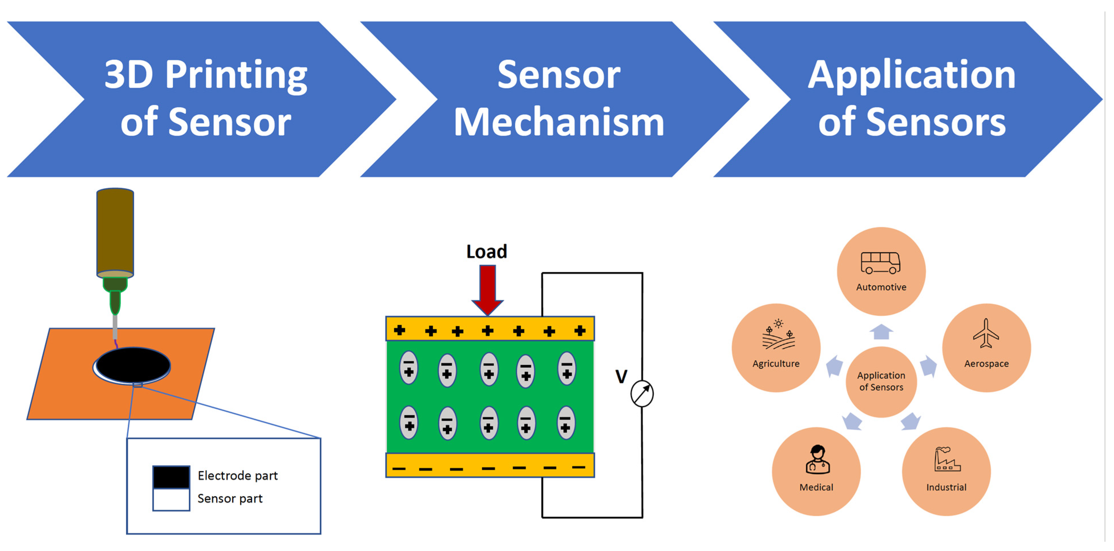
:1. Introduction
2. Sensing Mechanism and Type
2.1. Transducing
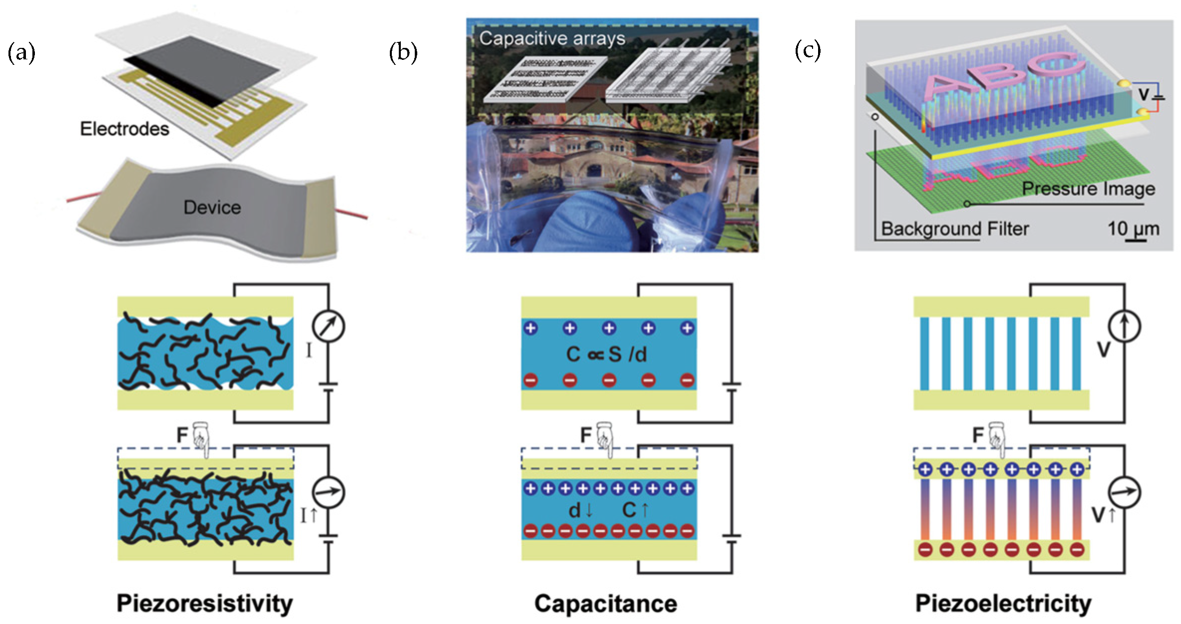
2.1.1. Piezoresistivity

| Methods | Printed Materials | Mechanism | Applications | Ref. |
|---|---|---|---|---|
| FFF | Thermoplastic elastomer | Capacitive | Force sensor | [42] |
| TPU/PLA/Carbon black | Capacitive, Resistive | Mechanical and tactile sensing | [17] | |
| Polyphenylsulfone/Polycarbonate | Capacitive | Biomedical sensing, human interface devices, material sensing | [43] | |
| PA12/Magnetic particle | Magnetic | Magnetic sensor application | [44] | |
| DIW | Sensor: TPU/Carbon black, Electrode: TPU/Ag | Piezoresistive | Skin-attachable electronics, human–machine interfaces, and electronic skins | [41] |
| Silver with sacrificial ink | Inductive/capacitive | Food deterioration | [45] | |
| Graphene/PDMS and PTFE/PDMS | Electrical resistive | Smart textile | [46] | |
| Urethane Triacrylate/Methacrylic acid | Inductive/capacitive | Neuro-robotics and neuro-prosthetics | [47] | |
| Clay slurry | Capacitive | Relative humidity sensing | [48] | |
| LPBF | Type K thermocouple | Seebeck effect | Temperature sensing | [49] |
| SS 316L powder (Conductive material) | Magnetic | Structural health monitoring | [50] | |
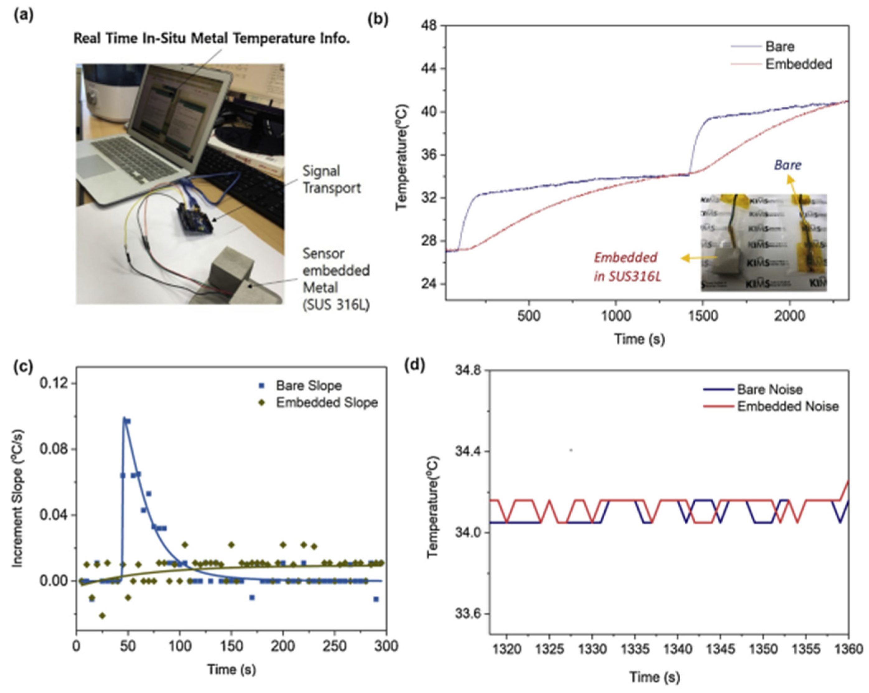
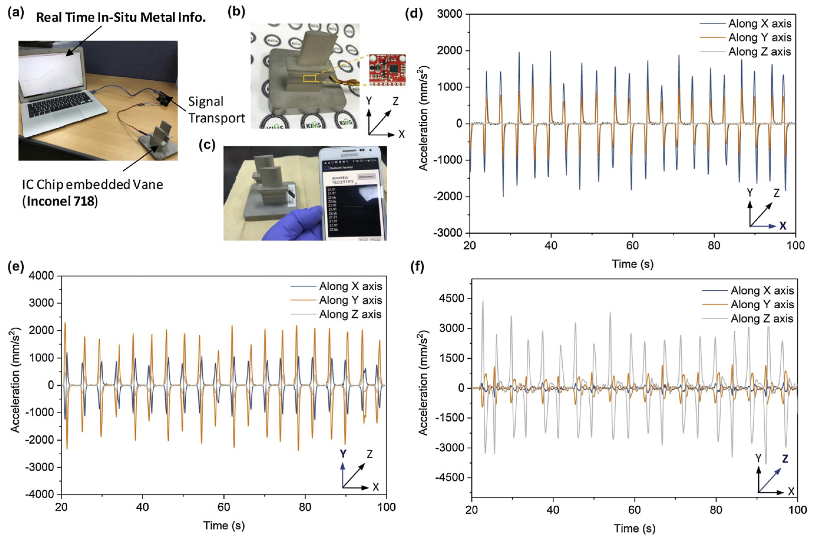
| SLM | SUS 316L, Inconel 718C | Thermal | Self-cognitive ability of metals | [51] |
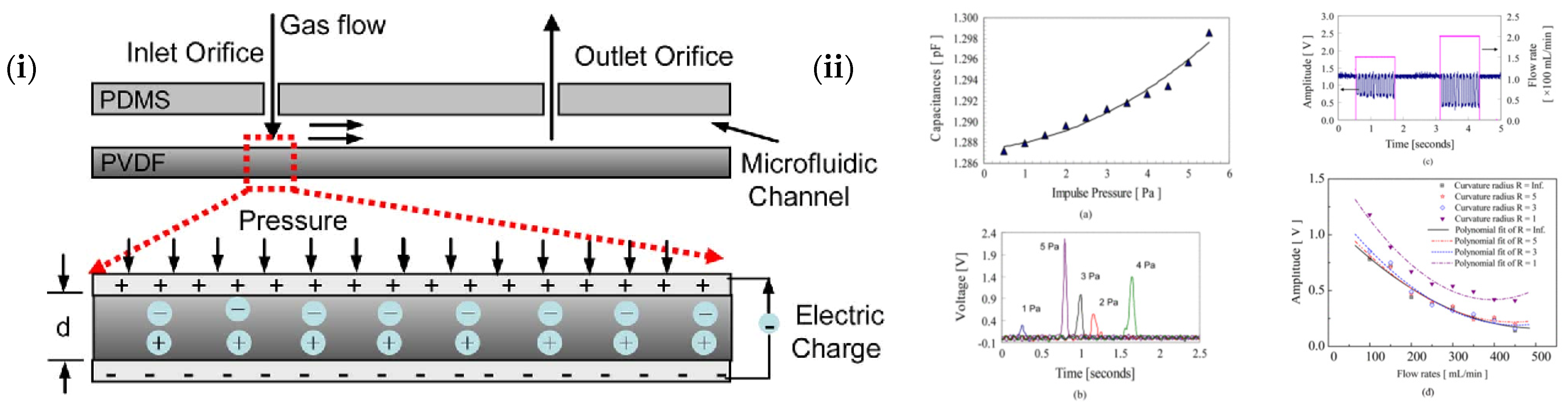
| SLA | PDMS | Electrochemical | Biologically active molecule sensing | [52] |
| Optical fiber | Pulse-calling | Particle analysis | [53] | |
| DLP | Elastomer | Piezoresistive | Tactile sensor | [52] |
| SP-RF0900 | Resistive | Robotic manipulation | [54] | |
| Resin | Capacitive | Particulate matter sensing | [55] | |
| DED | Ti-6AL-4V | Magnetic | Eddy current test | [56] |
| Stainless Steel/Zirconia | Resistive | Structural health monitoring | [57] | |
| Inkjet | Tin oxide | Electrical resistive | Gas sensing | [34] |
| ZnO | Resistive | Gas sensing | [58] | |
| Acrylic rubber | Resistive | Robotic gripper | [59] | |
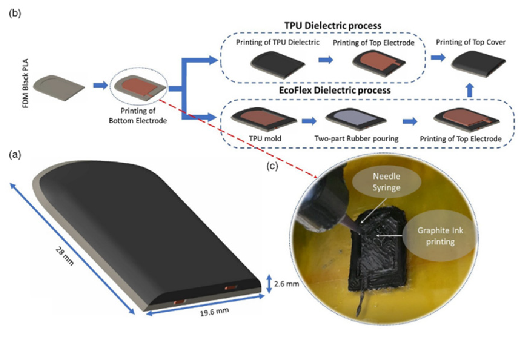
| FDM | TPU/graphite ink | Capacitive | Robotics | [60] |
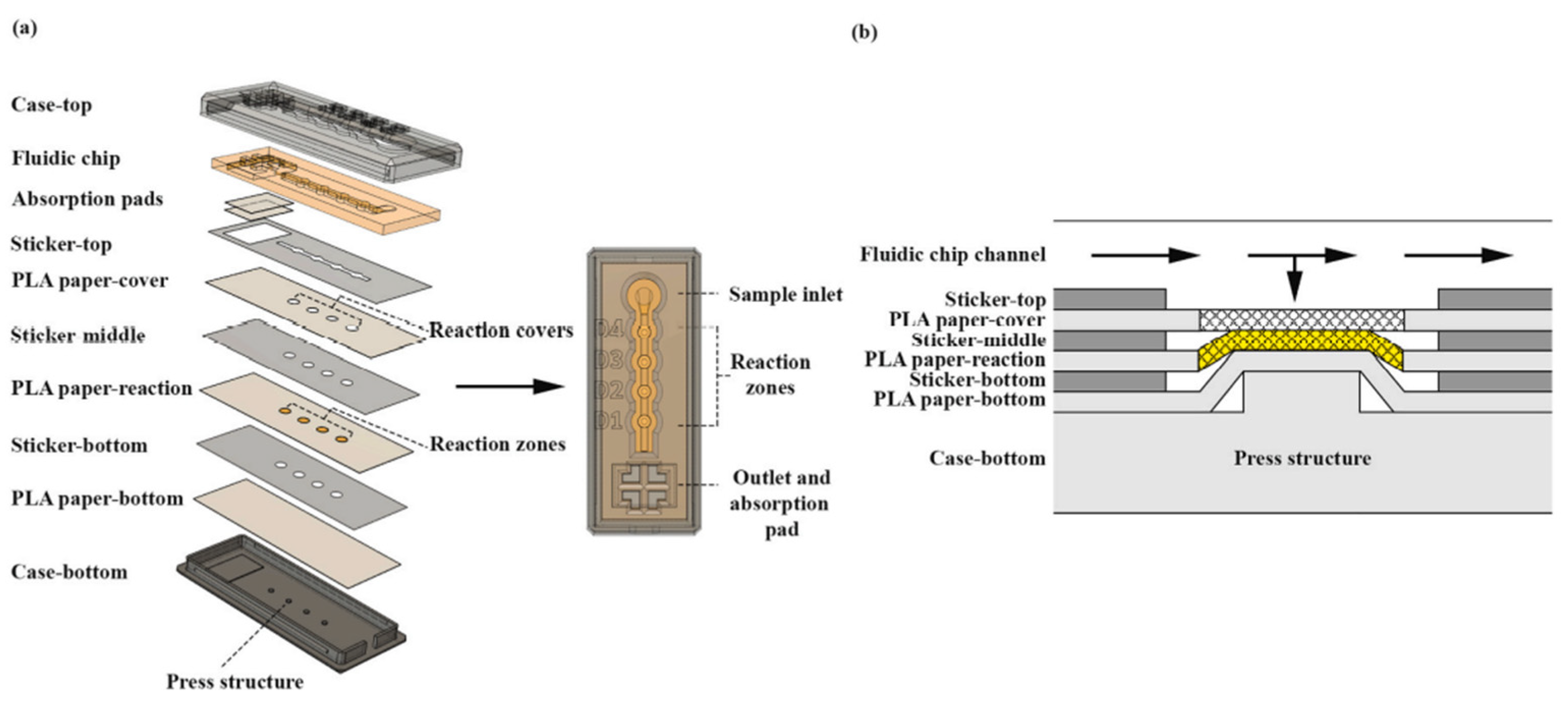
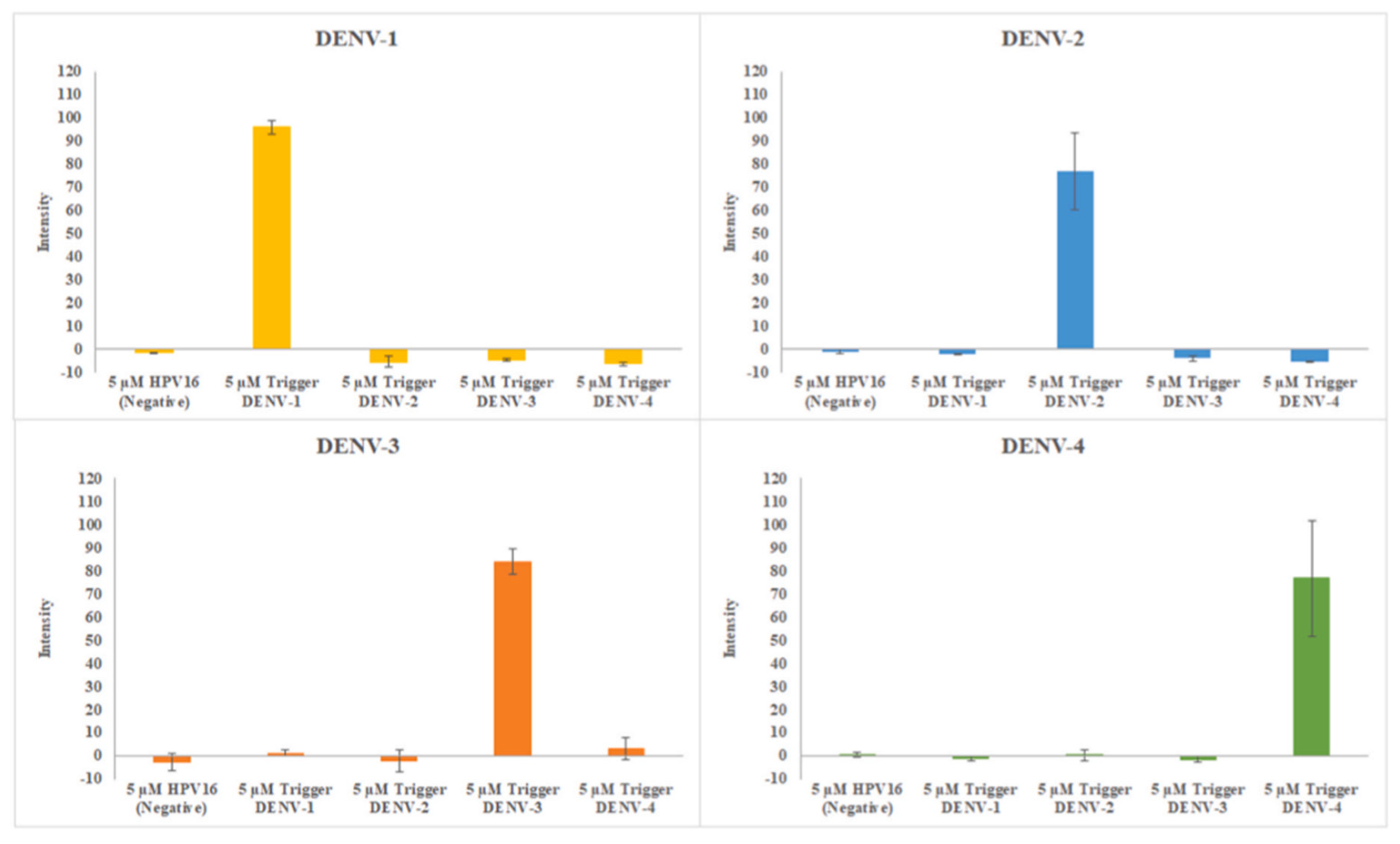
| PLA/wax filament | Nucleotide sequence | Dengue virus detection | [61] | |
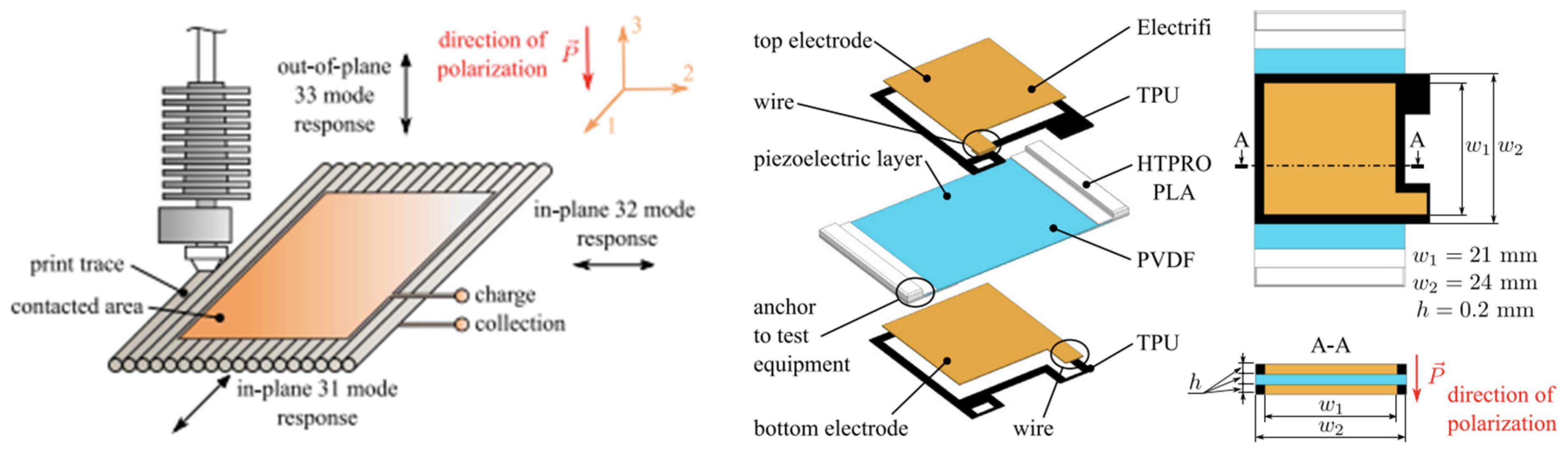
| BTO/MWCNT/PVDF | Piezoelectric | Energy storage | [62] | |
| BTO/PVDF | Piezoelectric | Pressure sensing | [63] |
2.1.2. Capacitance
2.1.3. Piezoelectricity
2.1.4. Magnetic Sensing
2.2. Wired
2.3. Wireless
3. Progress on 3D Printed Integrated Sensor
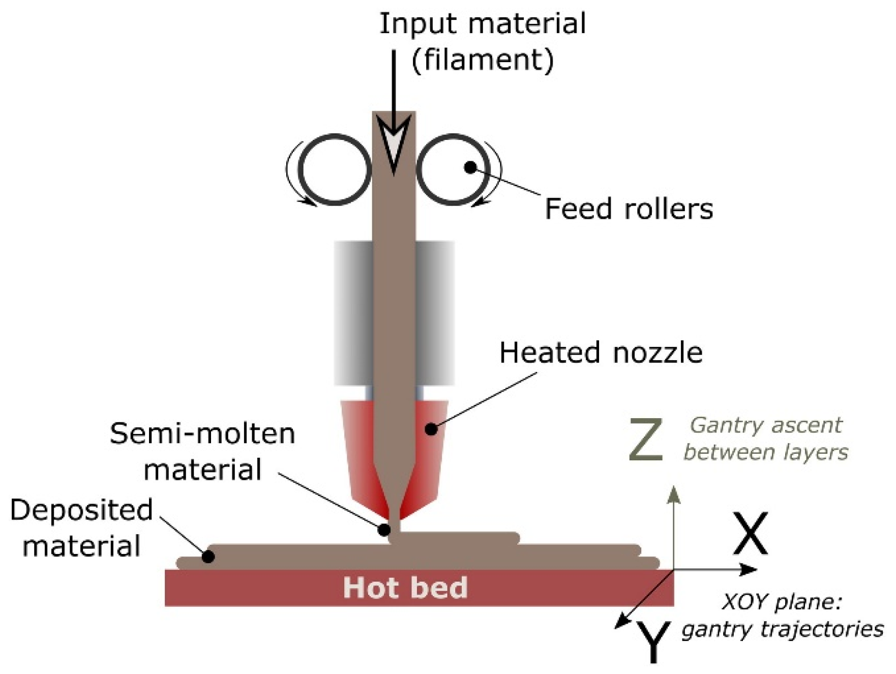
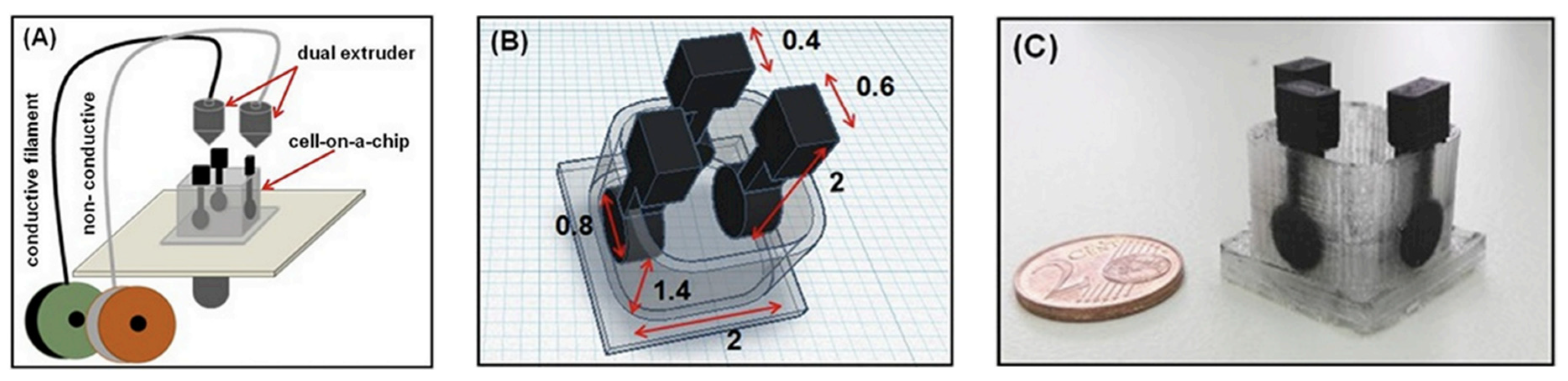
3.1. FFF Based 3D Printed Embedded Sensors
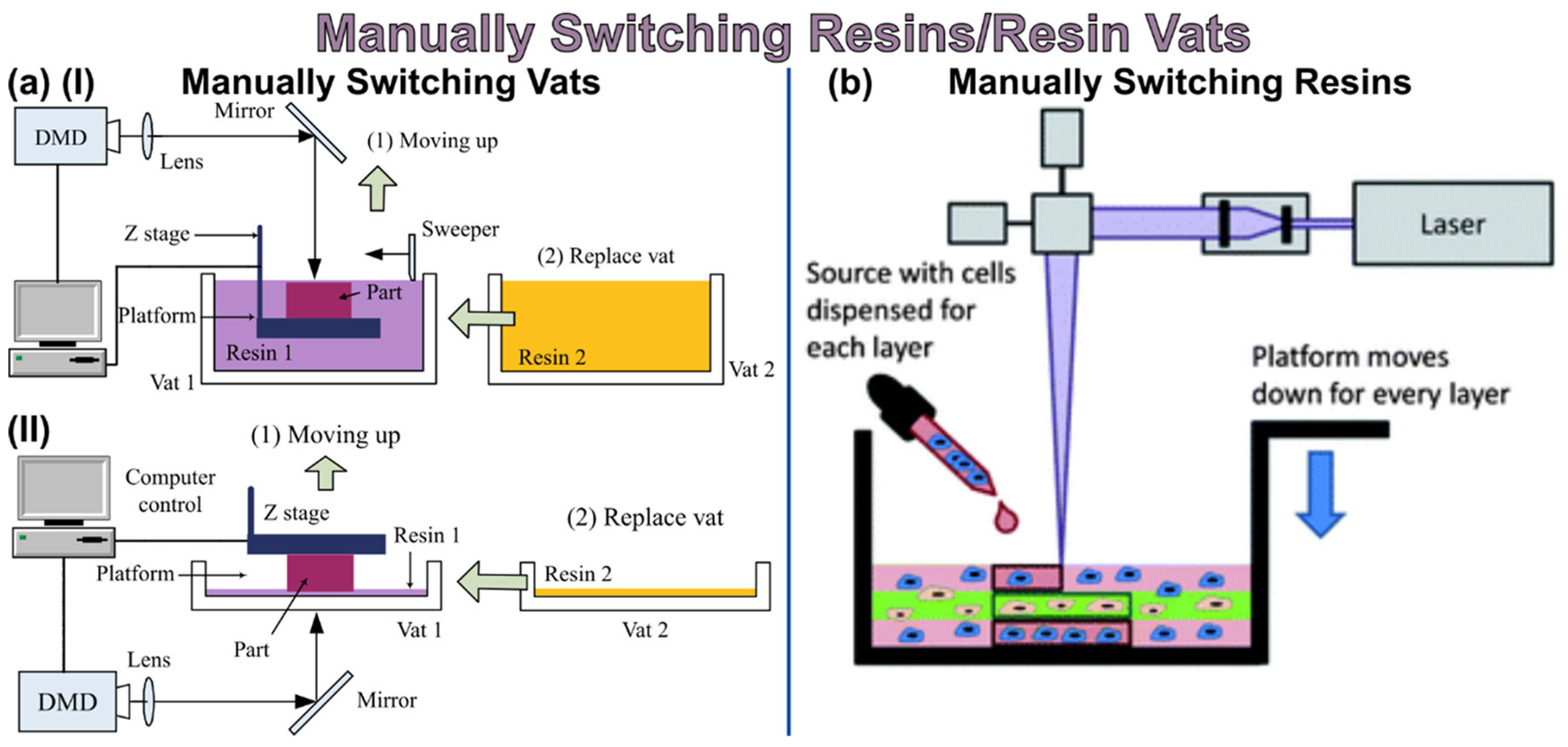
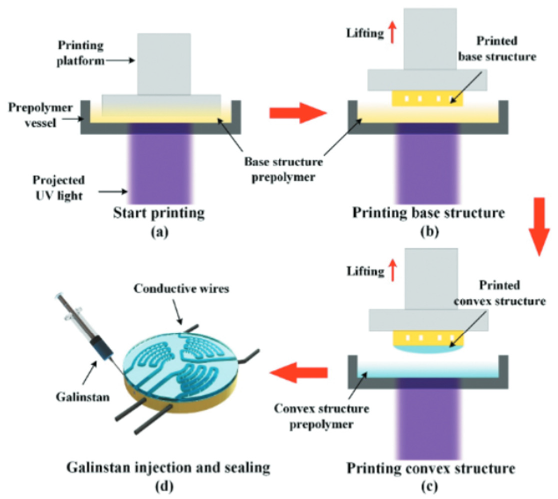
3.2. DLP/SLA Based 3D Printed Embedded Sensors
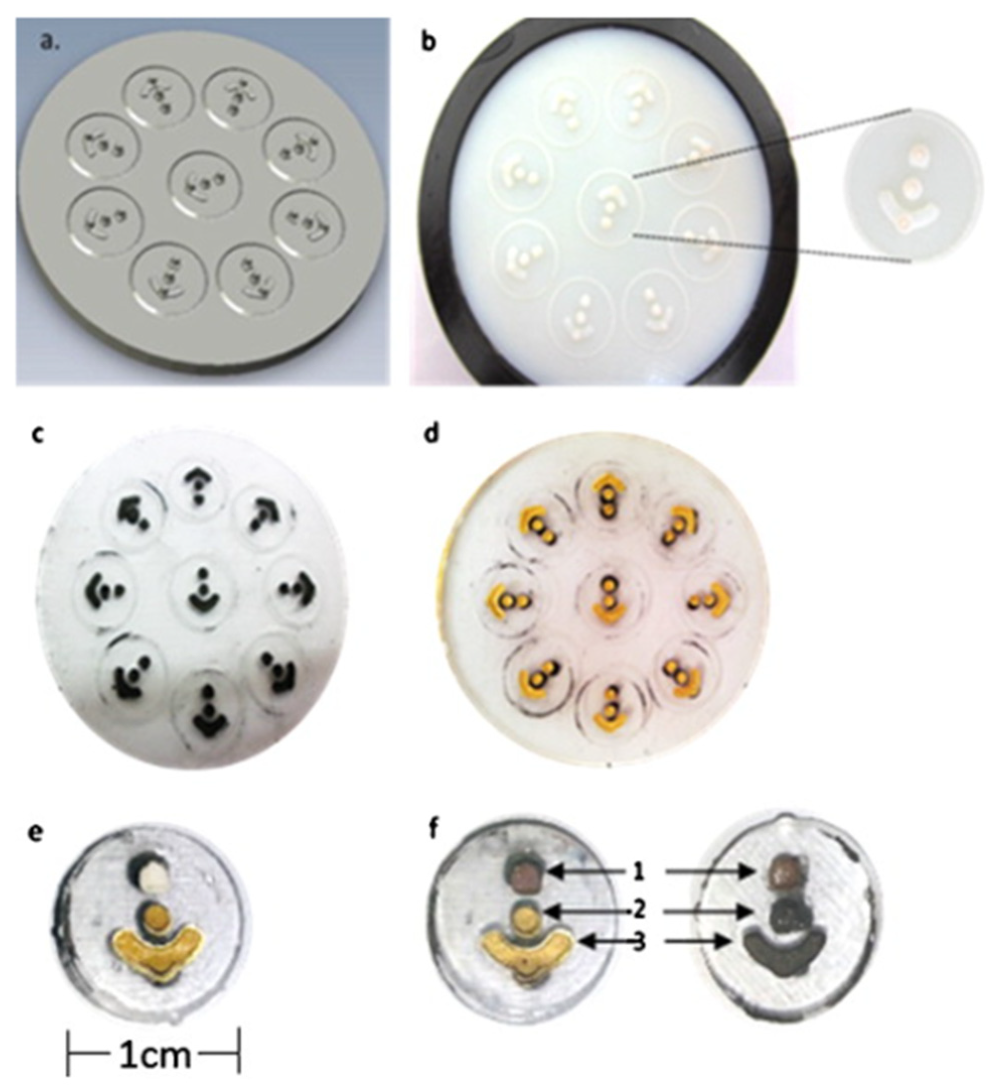
- (a)
- Manually stopping the print and changing vats/resins, as shown in Figure 8
- (b)
- Injecting material for each layer
- (c)
- Mechanical system changes vats/resins
- (d)
- Printing material around a complex, preexisting 3D structure
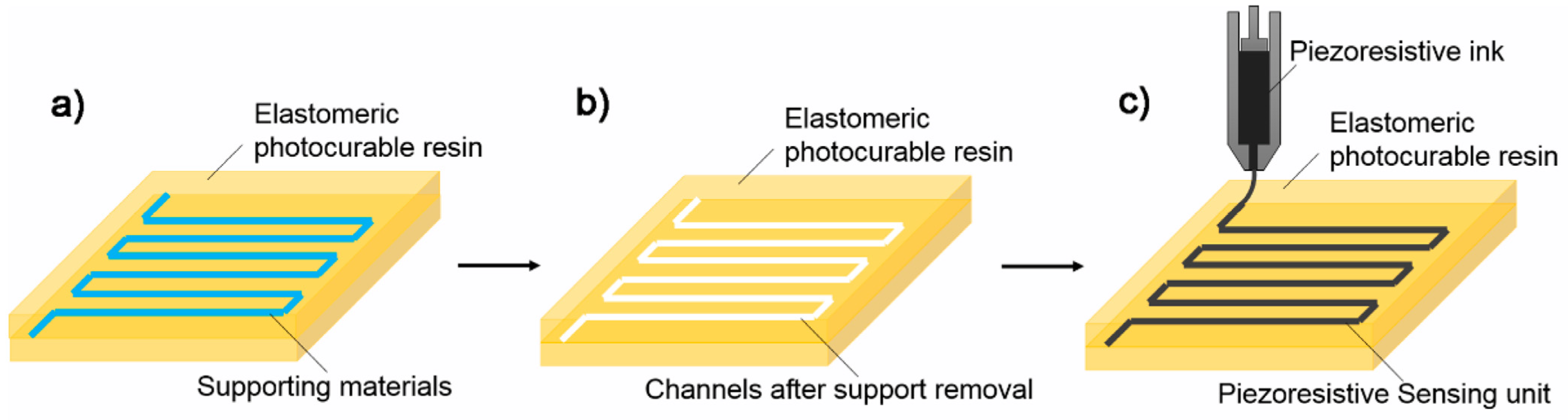
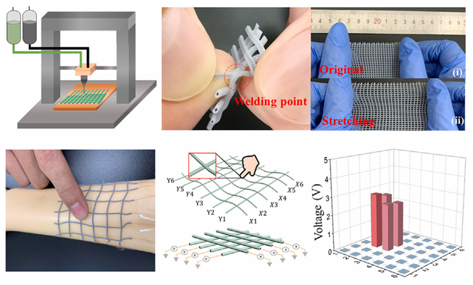
3.3. Direct Ink Write Technique
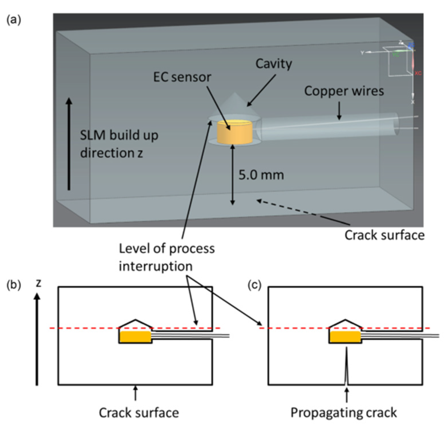
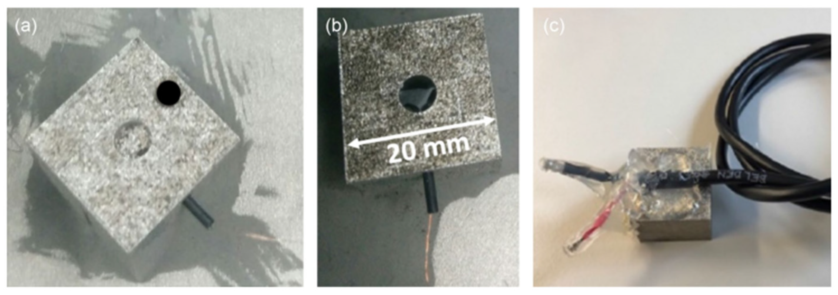
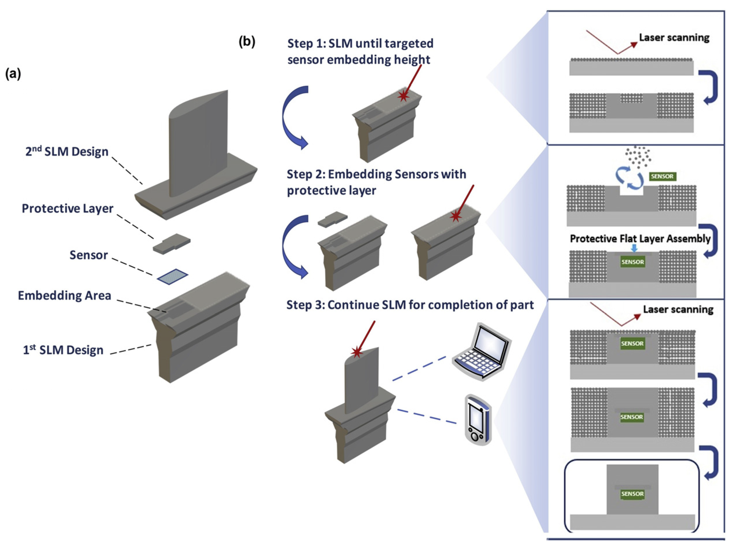
3.4. Laser Powder Based 3D Printed Embedded Sensors
3.5. DED Based 3D Printed Embedded Sensors
3.6. Inkjet Based 3D Printed Embedded Sensors
4. Integrated Physical Sensors and Their Applications
4.1. Piezoelectric Sensor
4.2. Piezoresistive Sensor
4.3. Magnetic Sensor
4.4. Capacitive Sensor
4.5. Gas Sensor
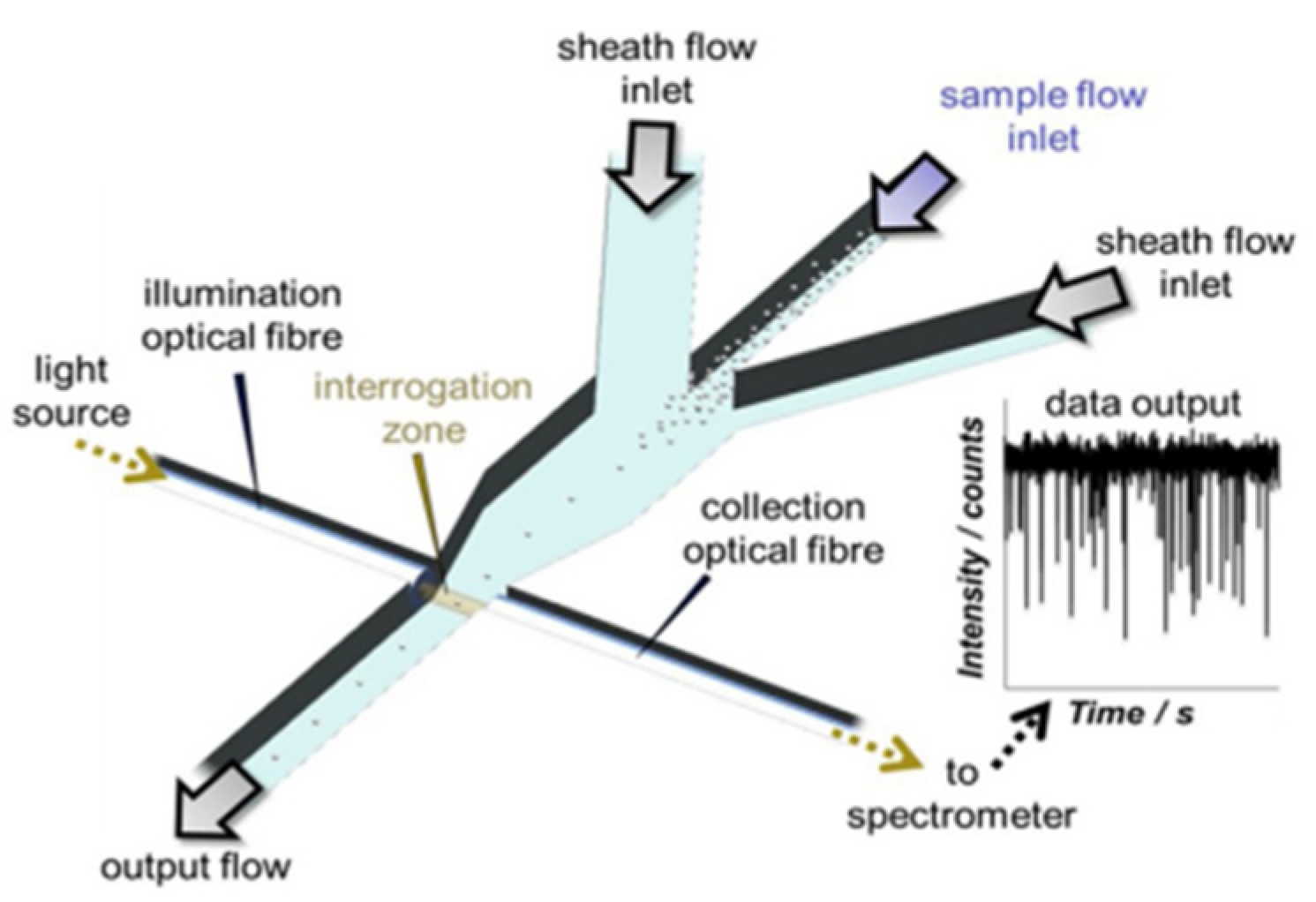
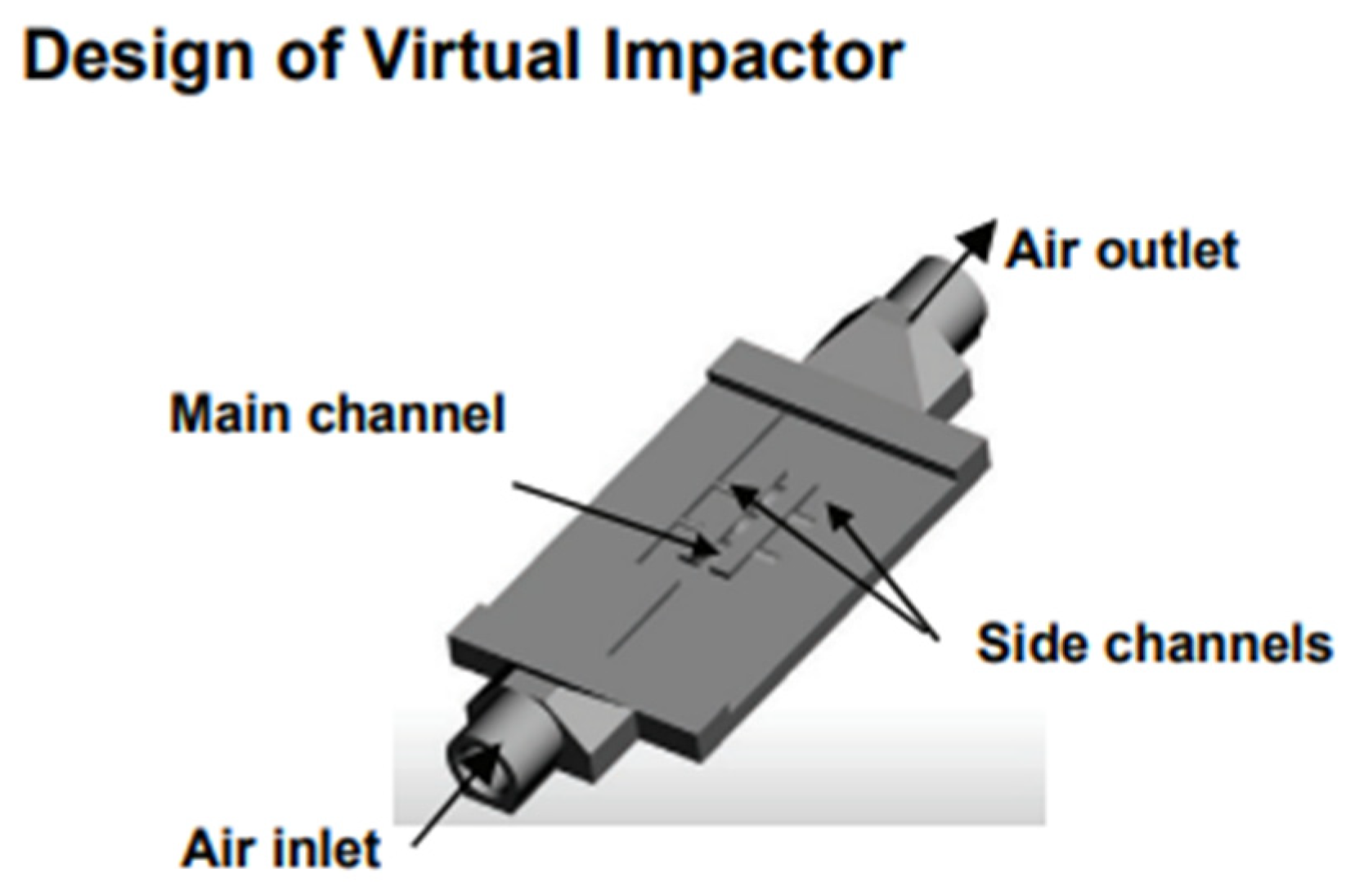
4.6. Particle Sensor
4.7. Tactile Sensor
4.8. Biosensors
4.9. Chemical Sensor
5. Challenges and Future Prospects
6. Conclusions
Author Contributions
Funding
Data Availability Statement
Conflicts of Interest
References
- Wang, C.H.; Liu, Y.; Desmulliez, M.; Richardson, A. Integrated sensors for health monitoring in advanced electronic systems. In Proceedings of the 2009 4th International Design and Test Workshop (IDT), Riyadh, Saudi Arabia, 15–17 November 2009; pp. 1–6. [Google Scholar]
- Qiu, K.; Zhao, Z.; Haghiashtiani, G.; Guo, S.-Z.; He, M.; Su, R.; Zhu, Z.; Bhuiyan, D.B.; Murugan, P.; Meng, F.; et al. 3D Printed Organ Models with Physical Properties of Tissue and Integrated Sensors. Adv. Mater. Technol. 2018, 3, 1700235. [Google Scholar] [CrossRef] [PubMed]
- Petrie, C.M.; Leonard, D.N.; Yang, Y.; Trammell, M.P.; Jolly, B.C.; Terrani, K. Embedment of Sensors in Ceramic Structures; Oak Ridge National Lab. (ORNL): Oak Ridge, TN, USA, 2019. [Google Scholar]
- Zaman, S.; Leyva, A.; Hassan, S.; Valladolid, A.; Herrera, N.E.; Gomez, S.G.; Mahmud, S.; Tucker, D.; Haynes, C.; Lin, Y. Implementation of Smart Materials for Actuation of Traditional Valve Technology for Hybrid Energy Systems. Actuators 2023, 12, 131. [Google Scholar] [CrossRef]
- Senesky, D.G.; Jamshidi, B.; Cheng, K.B.; Pisano, A.P. Harsh Environment Silicon Carbide Sensors for Health and Performance Monitoring of Aerospace Systems: A Review. IEEE Sens. J. 2009, 9, 1472–1478. [Google Scholar] [CrossRef]
- Additive Manufacturing Frontier: 3D Printing Electronics. Available online: https://www.oejournal.org/article/doi/10.29026/oea.2018.170004 (accessed on 16 November 2022).
- Veidt, M.; Liew, C.K. 17—Non-destructive evaluation (NDE) of aerospace composites: Structural health monitoring of aerospace structures using guided wave ultrasonics. In Non-Destructive Evaluation (NDE) of Polymer Matrix Composites; Karbhari, V.M., Ed.; Woodhead Publishing Series in Composites Science and Engineering; Woodhead Publishing: Sawston, UK, 2013; pp. 449–479. ISBN 978-0-85709-344-8. [Google Scholar]
- Talakokula, V.; Bhalla, S. Reinforcement corrosion assessment capability of surface bonded and embedded piezo sensors for reinforced concrete structures. J. Intell. Mater. Syst. Struct. 2015, 26, 2304–2313. [Google Scholar] [CrossRef]
- A Review paper on 3D-Printing Aspects and Various Processes Used in the 3D-Printing. Available online: https://www.researchgate.net/publication/350374850_A_Review_paper_on_3DPrinting_Aspects_and_Various_Processes_Used_in_the_3D-Printing (accessed on 16 November 2022).
- Attaran, M. The rise of 3-D printing: The advantages of additive manufacturing over traditional manufacturing. Bus. Horiz. 2017, 60, 677–688. [Google Scholar] [CrossRef]
- Pereira, T.; Kennedy, J.V.; Potgieter, J. A comparison of traditional manufacturing vs additive manufacturing, the best method for the job. Procedia Manuf. 2019, 30, 11–18. [Google Scholar] [CrossRef]
- Karayel, E.; Bozkurt, Y. Additive manufacturing method and different welding applications. J. Mater. Res. Technol. 2020, 9, 11424–11438. [Google Scholar] [CrossRef]
- Pérez, M.; Carou, D.; Rubio, E.M.; Teti, R. Current advances in additive manufacturing. Procedia CIRP 2020, 88, 439–444. [Google Scholar] [CrossRef]
- Shahrubudin, N.; Lee, T.C.; Ramlan, R. An Overview on 3D Printing Technology: Technological, Materials, and Applications. Procedia Manuf. 2019, 35, 1286–1296. [Google Scholar] [CrossRef]
- Regis, J.E.; Renteria, A.; Hall, S.E.; Hassan, S.; Marquez, C.; Lin, Y. Recent Trends and Innovation in Additive Manufacturing of Soft Functional Materials. Materials 2021, 14, 4521. [Google Scholar] [CrossRef] [PubMed]
- Renteria, A.; Balcorta, V.H.; Marquez, C.; Rodriguez, A.A.; Renteria-Marquez, I.; Regis, J.; Wilburn, B.; Patterson, S.; Espalin, D.; Tseng, T.-L.; et al. Direct ink write multi-material printing of PDMS-BTO composites with MWCNT electrodes for flexible force sensors. Flex. Print. Electron. 2022, 7, 015001. [Google Scholar] [CrossRef]
- Dijkshoorn, A.; Werkman, P.; Welleweerd, M.; Wolterink, G.; Eijking, B.; Delamare, J.; Sanders, R.; Krijnen, G.J.M. Embedded sensing: Integrating sensors in 3-D printed structures. J. Sensors Sens. Syst. 2018, 7, 169–181. [Google Scholar] [CrossRef]
- Emon, M.O.F.; Alkadi, F.; Philip, D.G.; Kim, D.-H.; Lee, K.-C.; Choi, J.-W. Multi-material 3D printing of a soft pressure sensor. Addit. Manuf. 2019, 28, 629–638. [Google Scholar] [CrossRef]
- Agarwala, S.; Goh, G.L.; Yap, Y.L.; Goh, G.D.; Yu, H.; Yeong, W.Y.; Tran, T. Development of bendable strain sensor with embedded microchannels using 3D printing. Sens. Actuators Phys. 2017, 263, 593–599. [Google Scholar] [CrossRef]
- Application of 3D Printing for Smart Objects with Embedded Electronic Sensors and Systems—Ota—2016—Advanced Materials Technologies—Wiley Online Library. Available online: https://onlinelibrary.wiley.com/doi/full/10.1002/admt.201600013 (accessed on 16 November 2022).
- Wu, S.-Y.; Yang, C.; Hsu, W.; Lin, L. 3D-printed microelectronics for integrated circuitry and passive wireless sensors. Microsyst. Nanoeng. 2015, 1, 15013. [Google Scholar] [CrossRef]
- Embedded 3D Printing of Strain Sensors within Highly Stretchable Elastomers—Muth—2014—Advanced Materials—Wiley Online Library. Available online: https://onlinelibrary.wiley.com/doi/10.1002/adma.201400334 (accessed on 16 November 2022).
- Nassar, H.; Ntagios, M.; Navaraj, W.T.; Dahiva, R. Multi-Material 3D Printed Bendable Smart Sensing Structures. In Proceedings of the 2018 IEEE SENSORS, New Delhi, India, 28–31 October 2018; 2018; pp. 1–4. [Google Scholar]
- Michelis, F.; Bodelot, L.; Bonnassieux, Y.; Lebental, B. Highly reproducible, hysteresis-free, flexible strain sensors by inkjet printing of carbon nanotubes. Carbon 2015, 95, 1020–1026. [Google Scholar] [CrossRef]
- Reig, C.; Avila-Navarro, E. Printed Antennas for Sensor Applications: A Review. IEEE Sensors J. 2013, 14, 2406–2418. [Google Scholar] [CrossRef]
- Sbriglia, L.R.; Baker, A.M.; Thompson, J.M.; Morgan, R.V.; Wachtor, A.J.; Bernardin, J.D. Embedding Sensors in FDM Plastic Parts During Additive Manufacturing. In Topics in Modal Analysis & Testing; Springer: Cham, Switzerland, 2016; Volume 10, pp. 205–214. [Google Scholar] [CrossRef]
- Shemelya, C.; Cedillos, F.; Aguilera, E.; Maestas, E.; Ramos, J.; Espalin, D.; Muse, D.; Wicker, R.; MacDonald, E. 3D printed capacitive sensors. In Proceedings of the Sensors, 2013 IEEE, Baltimore, MD, USA, 3–6 October 2013; pp. 1–4. [Google Scholar] [CrossRef]
- Hassan, S.; Chavez, L.A.; Chou, C.-C.; E Hall, S.; Tseng, T.-L.; Lin, Y. Mechanical response of shape-recovering metamaterial structures fabricated by additive manufacturing. Mater. Res. Express 2021, 8, 115801. [Google Scholar] [CrossRef]
- Stereolithography on Silicon for Microfluidics and Microsensor Packaging|SpringerLink. Available online: https://link.springer.com/article/10.1007/s00542-002-0254-y (accessed on 16 November 2022).
- Costa, B.M.d.C.; Griveau, S.; Bedioui, F.; Orlye, F.D.; da Silva, J.A.F.; Varenne, A. Stereolithography based 3D-printed microfluidic device with integrated electrochemical detection. Electrochim. Acta 2022, 407, 139888. [Google Scholar] [CrossRef]
- Cahill, V.; Taylor, D. Evaluation of Inkjet Technologies for Digital Fabrication & Functional Printing. Nip Digit. Fabr. Conf. 2012, 28, 12–44. [Google Scholar]
- Lu, R.; Arifuzzman, A.K.M.; Hossain, K.; Gardner, S.; Eliza, S.A.; Alexander, J.I.D.; Massoud, Y.; Haider, M.R. A Low-Power Sensitive Integrated Sensor System for Thermal Flow Monitoring. IEEE Trans. Very Large Scale Integr. Syst. 2019, 27, 2949–2953. [Google Scholar] [CrossRef]
- Humbert, A.; Tuerlings, B.J.; Hoofman, R.J.O.M.; Tan, Z.; Gravesteijn, D.; Pertijs, M.A.P.; Bastiaansen, C.W.M.; Soccol, D. A low-power CMOS integrated sensor for CO2 detection in the percentage range. In 2013 Transducers & Eurosensors XXVII: The 17th International Conference on Solid-State Sensors, Actuators and Microsystems (TRANSDUCERS & EUROSENSORS XXVII); Barcelona, Spain, 16–20 June 2013, pp. 1649–1652. [CrossRef]
- Juhasz, M.; Tiedemann, R.; Dumstorff, G.; Walker, J.; Du, P.A.; Conner, B.; Lang, W.; MacDonald, E. Hybrid directed energy deposition for fabricating metal structures with embedded sensors. Addit. Manuf. 2020, 35, 101397. [Google Scholar] [CrossRef]
- Integrating Fiber Optic Strain Sensors into Metal Using Ultrasonic Additive Manufacturing|SpringerLink. Available online: https://link.springer.com/article/10.1007/s11837-017-2709-8 (accessed on 16 November 2022).
- Hassan, M.S.; Billah, K.M.M.; Hall, S.E.; Sepulveda, S.; Regis, J.E.; Marquez, C.; Cordova, S.; Whitaker, J.; Robison, T.; Keating, J.; et al. Selective Laser Sintering of High-Temperature Thermoset Polymer. J. Compos. Sci. 2022, 6, 41. [Google Scholar] [CrossRef]
- Low-Temperature Selective Laser Sintering 3D Printing of PEEK-Nylon Blends: Impact of Thermal Post-Processing on Mechanical Properties and Thermal Stability—Chavez—2022—Journal of Applied Polymer Science—Wiley Online Library. Available online: https://onlinelibrary.wiley.com/doi/full/10.1002/app.52290 (accessed on 16 November 2022).
- Binder, M.; Kirchbichler, L.; Seidel, C.; Anstaett, C.; Schlick, G.; Reinhart, G. Design Concepts for the Integration of Electronic Components into Metal Laser-based Powder Bed Fusion Parts. Procedia CIRP 2019, 81, 992–997. [Google Scholar] [CrossRef]
- Algamili, A.S.; Khir, M.H.M.; Dennis, J.O.; Ahmed, A.Y.; Alabsi, S.S.; Hashwan, S.S.B.; Junaid, M.M. A Review of Actuation and Sensing Mechanisms in MEMS-Based Sensor Devices. Nanoscale Res. Lett. 2021, 16, 16. [Google Scholar] [CrossRef]
- Chung, D.D.L. A critical review of piezoresistivity and its application in electrical-resistance-based strain sensing. J. Mater. Sci. 2020, 55, 15367–15396. [Google Scholar] [CrossRef]
- Full 3D Printing of Stretchable Piezoresistive Sensor with Hierarchical Porosity and Multimodulus Architecture—Wang—2019—Advanced Functional Materials—Wiley Online Library. Available online: https://onlinelibrary.wiley.com/doi/abs/10.1002/adfm.201807569 (accessed on 29 November 2022).
- Fabrication and Analysis of a Composite 3D Printed Capacitive Force Sensor|3D Printing and Additive Manufacturing. Available online: https://www.liebertpub.com/doi/abs/10.1089/3dp.2016.0021 (accessed on 29 November 2022).
- Transduction Mechanisms, Micro-Structuring Techniques, and Applications of Electronic Skin Pressure Sensors: A Review of Recent Advances—PMC. Available online: https://www.ncbi.nlm.nih.gov/pmc/articles/PMC7472322/ (accessed on 29 November 2022).
- Huber, C.; Abert, C.; Bruckner, F.; Groenefeld, M.; Schuschnigg, S.; Teliban, I.; Vogler, C.; Wautischer, G.; Windl, R.; Suess, D. 3D Printing of Polymer-Bonded Rare-Earth Magnets with a Variable Magnetic Compound Fraction for a Predefined Stray Field. Sci. Rep. 2017, 7, 9419. [Google Scholar] [CrossRef]
- Wu, S.Y.; Yang, C.; Hsu, W.; Lin, L. RF wireless LC tank sensors fabricated by 3D additive manufacturing. In Proceedings of the 2015 Transducers-2015 18th International Conference on Solid-State Sensors, Actuators and Microsystems (TRANSDUCERS), Anchorage, AK, USA, 21–25 June 2015; pp. 2208–2211. [Google Scholar]
- Wang, Y.; Jin, J.; Lu, Y.; Mei, D. 3D Printing of Liquid Metal Based Tactile Sensor for Simultaneously Sensing of Temperature and Forces. Int. J. Smart Nano Mater. 2021, 12, 269–285. [Google Scholar] [CrossRef]
- Chen, Y.; Deng, Z.; Ouyang, R.; Zheng, R.; Jiang, Z.; Bai, H.; Xue, H. 3D printed stretchable smart fibers and textiles for self-powered e-skin. Nano Energy 2021, 84, 105866. [Google Scholar] [CrossRef]
- Marquez, C.; Mata, J.J.; Renteria, A.; Gonzalez, D.; Gomez, S.G.; Lopez, A.; Baca, A.N.; Nuñez, A.; Hassan, S.; Burke, V.; et al. Direct Ink-Write Printing of Ceramic Clay with an Embedded Wireless Temperature and Relative Humidity Sensor. Sensors 2023, 23, 3352. [Google Scholar] [CrossRef]
- Hassan, S.; Zaman, S.; Rodriguez, A.; Molina, L.; Dominguez, C.E.; Morgan, R.; Bernardin, J.; Lin, Y. Direct ink write 3D printing of wave propagation sensor. Flex. Print. Electron. 2022, 7, 045011. [Google Scholar] [CrossRef]
- Hyer, H.; Carver, K.; List, F., III; Petrie, C. Embedding Sensors in 3D Printed Metal Structures; ORNL/TM-2021/2143; Oak Ridge National Laboratory (ORNL): Oak Ridge, TN, USA. [CrossRef]
- Havermann, D.; Mathew, J.; Macpherson, W.N.; Maier, R.R.J.; Hand, D.P. In-situ strain sensing with fiber optic sensors embedded into stainless steel 316. Sens. Smart Struct. Technol. Civ. Mech. Aerosp. Syst. 2015, 9435, 94352W. [Google Scholar] [CrossRef]
- 3D Printed Strain Gauge Geometry and Orientation for Embedded Sensing|AIAA SciTech Forum. Available online: https://arc.aiaa.org/doi/10.2514/6.2017-0350 (accessed on 30 November 2022).
- Zhang, D.; Zhang, Z.; Wei, H.; Krishnaswamy, S. Highly sensitive Mach–Zehnder interferometric micromagnetic field sensor based on 3D printing technology. Appl. Opt. 2021, 60, 8493–8498. [Google Scholar] [CrossRef]
- Hossain, S.D.; Arif, A.; Lohani, B.; Roberts, R.C. Flexible EGaIn Liquid Metal Microstrip Patch Antenna Based Pressure Sensor. In Proceedings of the 2021 IEEE Sensors, Virtual, 31 October 2021; pp. 1–4. [Google Scholar] [CrossRef]
- Wang, C.; Yin, L.; Zhang, L.; Xiang, D.; Gao, R. Metal Oxide Gas Sensors: Sensitivity and Influencing Factors. Sensors 2010, 10, 2088–2106. [Google Scholar] [CrossRef] [PubMed]
- He, D.; Wang, Z.; Kusano, M.; Kishimoto, S.; Watanabe, M. Evaluation of 3D-Printed titanium alloy using eddy current testing with high-sensitivity magnetic sensor. NDT E Int. 2018, 102, 90–95. [Google Scholar] [CrossRef]
- Jung, I.D.; Lee, M.S.; Lee, J.; Sung, H.; Choe, J.; Son, H.J.; Yun, J.; Kim, K.-B.; Kim, M.; Lee, S.W.; et al. Embedding sensors using selective laser melting for self-cognitive metal parts. Addit. Manuf. 2020, 33, 101151. [Google Scholar] [CrossRef]
- Chang, C.-J.; Hung, S.-T.; Lin, C.-K.; Chen, C.-Y.; Kuo, E.-H. Selective growth of ZnO nanorods for gas sensors using ink-jet printing and hydrothermal processes. Thin Solid Films 2010, 519, 1693–1698. [Google Scholar] [CrossRef]
- Hampson, S.; Rowe, W.; Christie, S.; Platt, M. 3D printed microfluidic device with integrated optical sensing for particle analysis. Sensors Actuators B Chem. 2018, 256, 1030–1037. [Google Scholar] [CrossRef]
- Khosravani, M.R.; Reinicke, T. 3D-printed sensors: Current progress and future challenges. Sensors Actuators A Phys. 2020, 305, 111916. [Google Scholar] [CrossRef]
- Wang, H.; Cen, Y.; Zeng, X. Highly Sensitive Flexible Tactile Sensor Mimicking the Microstructure Perception Behavior of Human Skin. ACS Appl. Mater. Interfaces 2021, 13, 28538–28545. [Google Scholar] [CrossRef]
- Kim, H.; Islam, T.; Didarul, I.M.; Chavez, L.A.; Rosales, C.A.G.; Wilburn, B.R.; Stewart, C.M.; Noveron, J.C.; Tseng, T.-L.B.; Lin, Y. Increased piezoelectric response in functional nanocomposites through multiwall carbon nanotube interface and fused-deposition modeling three-dimensional printing. MRS Commun. 2017, 7, 960–966. [Google Scholar] [CrossRef]
- Kim, H.; Torres, F.; Wu, Y.; Villagran, D.; Lin, Y.; Tseng, T.-L. Integrated 3D printing and corona poling process of PVDF piezoelectric films for pressure sensor application. Smart Mater. Struct. 2017, 26, 085027. [Google Scholar] [CrossRef]
- Recent Progress in Electronic Skin—Wang—2015—Advanced Science—Wiley Online Library. Available online: https://onlinelibrary.wiley.com/doi/full/10.1002/advs.201500169 (accessed on 29 November 2022).
- Additive Manufacturing of Piezoelectric Materials—Chen—2020—Advanced Functional Materials—Wiley Online Library. Available online: https://onlinelibrary.wiley.com/doi/10.1002/adfm.202005141 (accessed on 29 November 2022).
- A Comprehensive Review on Vibration Based Micro Power Generators Using Electromagnetic and Piezoelectric Transducer Mechanisms—ScienceDirect. Available online: https://www.sciencedirect.com/science/article/abs/pii/S0196890415009164?via%3Dihub (accessed on 29 November 2022).
- Three-Dimensional Printing of Piezoelectric Materials with Designed Anisotropy and Directional Response|Nature Materials. Available online: https://www.nature.com/articles/s41563-018-0268-1 (accessed on 29 November 2022).
- Zhang, C.; Li, X.; Jiang, L.; Tang, D.; Xu, H.; Zhao, P.; Fu, J.; Zhou, Q.; Chen, Y. 3D Printing of Functional Magnetic Materials: From Design to Applications. Adv. Funct. Mater. 2021, 31, 2102777. [Google Scholar] [CrossRef]
- Credi, C.; Fiorese, A.; Tironi, M.; Bernasconi, R.; Magagnin, L.; Levi, M.; Turri, S. 3D Printing of Cantilever-Type Microstructures by Stereolithography of Ferromagnetic Photopolymers. ACS Appl. Mater. Interfaces 2016, 8, 26332–26342. [Google Scholar] [CrossRef] [PubMed]
- Chizari, K.; Daoud, M.A.; Ravindran, A.R.; Therriault, D. 3D Printing of Highly Conductive Nanocomposites for the Functional Optimization of Liquid Sensors. Small 2016, 12, 6076–6082. [Google Scholar] [CrossRef] [PubMed]
- Mu, Q.; Dunn, C.K.; Wang, L.; Dunn, M.L.; Qi, H.J.; Wang, T. Thermal cure effects on electromechanical properties of conductive wires by direct ink write for 4D printing and soft machines. Smart Mater. Struct. 2017, 26, 045008. [Google Scholar] [CrossRef]
- Hill, J.; Culler, D. A wireless embedded sensor architecture for system-level optimization. In UC Berkeley Technical Report; Berkeley EECS: Berkeley, CA, USA, 2002; pp. 1–2. [Google Scholar]
- Farooqui, M.F.; Karimi, M.A.; Salama, K.N.; Shamim, A. 3D-Printed Disposable Wireless Sensors with Integrated Microelectronics for Large Area Environmental Monitoring. Adv. Mater. Technol. 2017, 2, 1700051. [Google Scholar] [CrossRef]
- Herbert, R.; Mishra, S.; Lim, H.; Yoo, H.; Yeo, W. Fully Printed, Wireless, Stretchable Implantable Biosystem toward Batteryless, Real-Time Monitoring of Cerebral Aneurysm Hemodynamics. Adv. Sci. 2019, 6, 1901034. [Google Scholar] [CrossRef]
- Kalhori, A.H.; Kim, T.; Kim, W.S. Enhanced RF response of 3D-printed wireless LC sensors using dielectrics with high permittivity. Flex. Print. Electron. 2023, 8, 015013. [Google Scholar] [CrossRef]
- Parker, K.E.; Lee, J.; Kim, J.R.; Kawakami, C.; Kim, C.Y.; Qazi, R.; Jang, K.-I.; Jeong, J.-W.; McCall, J.G. Customizable, wireless and implantable neural probe design and fabrication via 3D printing. Nat. Protoc. 2022, 18, 3–21. [Google Scholar] [CrossRef] [PubMed]
- Herbert, R.; Lim, H.-R.; Rigo, B.; Yeo, W.-H. Fully implantable wireless batteryless vascular electronics with printed soft sensors for multiplex sensing of hemodynamics. Sci. Adv. 2022, 8, eabm1175. [Google Scholar] [CrossRef] [PubMed]
- Rigo, B.; Bateman, A.; Lee, J.; Kim, H.; Lee, Y.; Romero, L.; Jang, Y.C.; Herbert, R.; Yeo, W.-H. Soft implantable printed bioelectronic system for wireless continuous monitoring of restenosis. Biosens. Bioelectron. 2023, 241, 115650. [Google Scholar] [CrossRef]
- Fatigue Performance of Fused Filament Fabrication PLA Specimens—ScienceDirect. Available online: https://www.sciencedirect.com/science/article/pii/S0264127517311036 (accessed on 30 November 2022).
- Single-Process Fused Filament Fabrication 3D-Printed High-Sensitivity Dynamic Piezoelectric Sensor—ScienceDirect. Available online: https://www.sciencedirect.com/science/article/pii/S2214860421006291 (accessed on 30 November 2022).
- Katseli, V.; Economou, A.; Kokkinos, C. A novel all-3D-printed cell-on-a-chip device as a useful electroanalytical tool: Application to the simultaneous voltammetric determination of caffeine and paracetamol. Talanta 2020, 208, 120388. [Google Scholar] [CrossRef] [PubMed]
- Liu, C.; Huang, N.; Xu, F.; Tong, J.; Chen, Z.; Gui, X.; Fu, Y.; Lao, C. 3D printing technologies for flexible tactile sensors toward wearable electronics and electronic skin. Polymers 2018, 10, 629. [Google Scholar] [CrossRef]
- Ragones, H.; Schreiber, D.; Inberg, A.; Berkh, O.; Kósa, G.; Freeman, A.; Shacham-Diamand, Y. Disposable electrochemical sensor prepared using 3D printing for cell and tissue diagnostics. Sensors Actuators B Chem. 2015, 216, 434–442. [Google Scholar] [CrossRef]
- Hossain, S.D.; Mora, M.A.P.; Arif, A.; Lohani, B.; Roberts, R.C. Flexible Chipless RFID Temperature Memory Sensor. In Proceedings of the 2022 IEEE International Conference on Flexible and Printable Sensors and Systems (FLEPS), Vienna, Austria, 10–13 July 2022; pp. 1–4. [Google Scholar] [CrossRef]
- Multimaterial Vat Polymerization Additive Manufacturing|ACS Applied Polymer Materials. Available online: https://pubs.acs.org/doi/full/10.1021/acsapm.1c00262?casa_token=R3opT6oCAiUAAAAA%3AHLZBgRFCTGHFagfDUndrL7cEgzJ7EN9hN7Lkdo7qZJI9Lzz7QyaJV3TMOXfnMl33ihmaItb7woGJupjWNw (accessed on 30 November 2022).
- Shahzad, A.; Lazoglu, I. Direct ink writing (DIW) of structural and functional ceramics: Recent achievements and future challenges. Compos. Part B Eng. 2021, 225, 109249. [Google Scholar] [CrossRef]
- Schouten, M.; Wolterink, G.; Dijkshoorn, A.; Kosmas, D.; Stramigioli, S.; Krijnen, G. A Review of Extrusion-Based 3D Printing for the Fabrication of Electro- and Biomechanical Sensors. IEEE Sensors J. 2020, 21, 12900–12912. [Google Scholar] [CrossRef]
- Skylar-Scott, M.A.; Gunasekaran, S.; Lewis, J.A. Laser-assisted direct ink writing of planar and 3D metal architectures. Proc. Natl. Acad. Sci. USA 2016, 113, 6137–6142. [Google Scholar] [CrossRef]
- Revelo, C.F.; Colorado, H.A. 3D printing of kaolinite clay ceramics using the Direct Ink Writing (DIW) technique. Ceram. Int. 2018, 44, 5673–5682. [Google Scholar] [CrossRef]
- Rosenthal, M.; Henneberger, C.; Gutkes, A.; Bues, C.-T. Liquid Deposition Modeling: A promising approach for 3D printing of wood. Eur. J. Wood Wood Prod. 2017, 76, 797–799. [Google Scholar] [CrossRef]
- Lee, A.; Hudson, A.R.; Shiwarski, D.J.; Tashman, J.W.; Hinton, T.J.; Yerneni, S.; Bliley, J.M.; Campbell, P.G.; Feinberg, A.W. 3D bioprinting of collagen to rebuild components of the human heart. Science 2019, 365, 482–487. [Google Scholar] [CrossRef]
- Mannoor, M.S.; Jiang, Z.; James, T.; Kong, Y.L.; Malatesta, K.A.; Soboyejo, W.O.; Verma, N.; Gracias, D.H.; McAlpine, M.C. 3D Printed Bionic Ears. Nano Lett. 2013, 13, 2634–2639. [Google Scholar] [CrossRef] [PubMed]
- Murphy, S.V.; Atala, A. 3D bioprinting of tissues and organs. Nat. Biotechnol. 2014, 32, 773–785. [Google Scholar] [CrossRef] [PubMed]
- 3D Printable Ceramic–Polymer Electrolytes for Flexible High-Performance Li-Ion Batteries with Enhanced Thermal Stability—Blake—2017—Advanced Energy Materials—Wiley Online Library. Available online: https://onlinelibrary.wiley.com/doi/10.1002/aenm.201602920 (accessed on 8 February 2022).
- Wei, M.; Zhang, F.; Wang, W.; Alexandridis, P.; Zhou, C.; Wu, G. 3D direct writing fabrication of electrodes for electrochemical storage devices. J. Power Sources 2017, 354, 134–147. [Google Scholar] [CrossRef]
- 3D Printing of Customized Li-Ion Batteries with Thick Electrodes—Wei—2018—Advanced Materials—Wiley Online Library. Available online: https://onlinelibrary.wiley.com/doi/full/10.1002/adma.201703027 (accessed on 8 February 2022).
- 3D-Printing of Lightweight Cellular Composites—Compton—2014—Advanced Materials—Wiley Online Library. Available online: https://onlinelibrary.wiley.com/doi/10.1002/adma.201401804 (accessed on 8 February 2022).
- Feilden, E.; Ferraro, C.; Zhang, Q.; García-Tuñón, E.; D’elia, E.; Giuliani, F.; Vandeperre, L.; Saiz, E. 3D Printing Bioinspired Ceramic Composites. Sci. Rep. 2017, 7, 13759. [Google Scholar] [CrossRef]
- Kim, S.; Oh, J.; Jeong, D.; Park, W.; Bae, J. Consistent and Reproducible Direct Ink Writing of Eutectic Gallium–Indium for High-Quality Soft Sensors. Soft Robot. 2018, 5, 601–612. [Google Scholar] [CrossRef]
- An Integrated Design and Fabrication Strategy for Entirely Soft, Autonomous Robots|Nature. Available online: https://www.nature.com/articles/nature19100 (accessed on 9 February 2022).
- Bijender; Kumar, A. Flexible and wearable capacitive pressure sensor for blood pressure monitoring. Sens. Bio-Sensing Res. 2021, 33, 100434. [Google Scholar] [CrossRef]
- Vatani, M.; Engeberg, E.D.; Choi, J.-W. Conformal direct-print of piezoresistive polymer/nanocomposites for compliant multi-layer tactile sensors. Addit. Manuf. 2015, 7, 73–82. [Google Scholar] [CrossRef]
- Parekh, D.P.; Ladd, C.; Panich, L.; Moussa, K.; Dickey, M.D. 3D printing of liquid metals as fugitive inks for fabrication of 3D microfluidic channels. Lab a Chip 2016, 16, 1812–1820. [Google Scholar] [CrossRef]
- Stoll, P.; Gasparin, E.; Spierings, A.; Wegener, K. Embedding Eddy Current Sensors into LPBF Components for Structural Health Monitoring|SpringerLink. Available online: https://link.springer.com/article/10.1007/s40964-021-00204-3 (accessed on 11 February 2023).
- Hyer, H.C.; Petrie, C.M. Embedding Sensors in Stainless Steel Using Laser Powder Bed Fusion; Oak Ridge National Laboratory (ORNL): Oak Ridge, TN, USA, 2022; p. 1818670. [Google Scholar]
- Multicomponent and Multimaterials Printing—3D Printing for Energy Applications—Wiley Online Library. Available online: https://onlinelibrary.wiley.com/doi/abs/10.1002/9781119560807.ch5 (accessed on 6 April 2023).
- Carlota, V. The Complete Guide to Directed Energy Deposition (DED) in 3D Printing. 3Dnatives 2019. Available online: https://www.3dnatives.com/en/directed-energy-deposition-ded-3d-printing-guide-100920194/ (accessed on 11 February 2023).
- Gibson, I.; Rosen, D.; Stucker, B. Directed Energy Deposition Processes. In Additive Manufacturing Technologies: 3D Printing, Rapid Prototyping, and Direct Digital Manufacturing; Gibson, I., Rosen, D., Stucker, B., Eds.; Springer: New York, NY, USA, 2015; pp. 245–268. [Google Scholar] [CrossRef]
- Kim, S.I.; Jung, H.Y.; Yang, S.; Yoon, J.; Lee, H.; Ryu, W. 3D Printing of a miniature turbine blade model with an embedded fibre Bragg grating sensor for high-temperature monitoring. Virtual Phys. Prototyp. 2021, 17, 156–169. [Google Scholar] [CrossRef]
- Al-Halhouli, A.; Qitouqa, H.; Alashqar, A.; Abu-Khalaf, J. Inkjet printing for the fabrication of flexible/stretchable wearable electronic devices and sensors. Sens. Rev. 2018, 38, 438–452. [Google Scholar] [CrossRef]
- Piłczyńska, K. Material jetting. Polym. 3d Print. 2022, 91–103. [Google Scholar] [CrossRef]
- Andò, B.; Marletta, V. An All-InkJet Printed Bending Actuator with Embedded Sensing Feature and an Electromagnetic Driving Mechanism. Actuators 2016, 5, 21. [Google Scholar] [CrossRef]
- Pinto, T.; Chen, C.; Pinger, C.; Tan, X. 3D-printed liquid metal-based stretchable conductors and pressure sensors. Smart Mater. Struct. 2021, 30, 095005. [Google Scholar] [CrossRef]
- Mieloszyk, M.; Andrearczyk, A.; Majewska, K.; Jurek, M.; Ostachowicz, W. Polymeric structure with embedded fiber Bragg grating sensor manufactured using multi-jet printing method. Measurement 2020, 166, 108229. [Google Scholar] [CrossRef]
- Benes, E.; Gröschl, M.; Burger, W.; Schmid, M. Sensors based on piezoelectric resonators. Sens. Actuators A Phys. 1995, 48, 1–21. [Google Scholar] [CrossRef]
- He, L.; Wang, B.; Wen, Z.; Li, X.; Wu, D. 3-D High Frequency Ultrasound Imaging by Piezo-Driving a Single-Element Transducer. IEEE Trans. Ultrason. Ferroelectr. Freq. Control. 2022, 69, 1932–1942. [Google Scholar] [CrossRef] [PubMed]
- Sezer, N.; Koç, M. A comprehensive review on the state-of-the-art of piezoelectric energy harvesting. Nano Energy 2020, 80, 105567. [Google Scholar] [CrossRef]
- Covaci, C.; Gontean, A. Piezoelectric energy harvesting solutions: A review. Sensors 2020, 20, 3512. [Google Scholar] [CrossRef]
- Jiang, L.; Yang, Y.; Chen, Y.; Zhou, Q. Ultrasound-induced wireless energy harvesting: From materials strategies to functional applications. Nano Energy 2020, 77, 105131. [Google Scholar] [CrossRef]
- Cross, L.E.; Heywang, W. Piezoelectricity Evolution and Future of a Technology Introduction. Piezoelectricity 2008, 114, 1–5. [Google Scholar]
- Tadigadapa, S.A.; Mateti, K. Piezoelectric MEMS sensors: State-of-the-art and perspectives. Meas. Sci. Technol. 2009, 20, 092001. [Google Scholar] [CrossRef]
- Chen, Z.; Song, X.; Lei, L.; Chen, X.; Fei, C.; Chiu, C.T.; Qian, X.; Ma, T.; Yang, Y.; Shung, K.; et al. 3D printing of piezoelectric element for energy focusing and ultrasonic sensing. Nano Energy 2016, 27, 78–86. [Google Scholar] [CrossRef]
- Tariverdian, T.; Behnamghader, A.; Milan, P.B.; Barzegar-Bafrooei, H.; Mozafari, M. 3D-printed barium strontium titanate-based piezoelectric scaffolds for bone tissue engineering. Ceram. Int. 2019, 45, 14029–14038. [Google Scholar] [CrossRef]
- Chang, W.-Y.; Chu, C.-H.; Lin, Y.-C. A Flexible Piezoelectric Sensor for Microfluidic Applications Using Polyvinylidene Fluoride. IEEE Sensors J. 2008, 8, 495–500. [Google Scholar] [CrossRef]
- Fiorillo, A.; Critello, C.; Pullano, S. Theory, technology and applications of piezoresistive sensors: A review. Sensors Actuators A: Phys. 2018, 281, 156–175. [Google Scholar] [CrossRef]
- Pagliano, S.; Marschner, D.E.; Maillard, D.; Ehrmann, N.; Stemme, G.; Braun, S.; Villanueva, L.G.; Niklaus, F. Micro 3D printing of a functional MEMS accelerometer. Microsyst. Nanoeng. 2022, 8, 105. [Google Scholar] [CrossRef]
- Emon, M.O.; Choi, J.W. Flexible piezoresistive sensors embedded in 3D printed tires. Sensors 2017, 17, 656. [Google Scholar] [CrossRef]
- Li, T.; Jayawardhana, B.; Kamat, A.M.; Kottapalli, A.G.P. Source-Seeking Control of Unicycle Robots with 3-D-Printed Flexible Piezoresistive Sensors. IEEE Trans. Robot. 2021, 38, 448–462. [Google Scholar] [CrossRef]
- Song, D.; Chen, X.; Wang, M.; Wu, Z.; Xiao, X. 3D-printed flexible sensors for food monitoring. Chem. Eng. J. 2023, 474, 146011. [Google Scholar] [CrossRef]
- Hohimer, C.J.; Petrossian, G.; Ameli, A.; Mo, C.; Pötschke, P. 3D printed conductive thermoplastic polyurethane/carbon nanotube composites for capacitive and piezoresistive sensing in soft pneumatic actuators. Addit. Manuf. 2020, 34, 101281. [Google Scholar] [CrossRef]
- Fekiri, C.; Kim, H.C.; Lee, I.H. 3D-Printable Carbon Nanotubes-Based Composite for Flexible Piezoresistive Sensors. Materials 2020, 13, 5482. [Google Scholar] [CrossRef] [PubMed]
- Wouters, C.; Vranković, V.; Rössler, C.; Sidorov, S.; Ensslin, K.; Wegscheider, W.; Hierold, C. Design and fabrication of an innovative three-axis Hall sensor. Sensors Actuators A Phys. 2015, 237, 62–71. [Google Scholar] [CrossRef]
- Chatzipirpiridis, G.; Erne, P.; Ergeneman, O.; Pane, S.; Nelson, B.J. A magnetic force sensor on a catheter tip for minimally invasive surgery. In Proceedings of the 37th Annual International Conference of the IEEE Engineering in Medicine and Biology Society (EMBC), Milan, Italy, 25–29 August 2015. [Google Scholar] [CrossRef]
- Olivas, R.; Salas, R.; Muse, D.; MacDonald, E.; Wicker, R.; Newton, M.; Church, K. Structural Electronics through Additive Manufacturing and Micro-Dispensing. Int. Symp. Microelectron. 2010, 2010, 000940–000946. [Google Scholar] [CrossRef]
- Saharan, L.K.; Agbesoyin, T. Design and 3D printing of a capacitive sensor for biomedical applications. In Proceedings of the Sensors and Smart Structures Technologies for Civil, Mechanical, and Aerospace Systems 2022, Long Beach, CA, USA, 6–10 March 2022; Volume 12046, pp. 333–338. [Google Scholar] [CrossRef]
- Stano, G.; Di Nisio, A.; Lanzolla, A.M.; Ragolia, M.A.; Percoco, G. Additive manufacturing for capacitive liquid level sensors. Int. J. Adv. Manuf. Technol. 2022, 123, 2519–2529. [Google Scholar] [CrossRef]
- Zhang, C.; Zheng, H.; Sun, J.; Zhou, Y.; Xu, W.; Dai, Y.; Mo, J.; Wang, Z. 3D Printed, Solid-State Conductive Ionoelastomer as a Generic Building Block for Tactile Applications. Adv. Mater. 2021, 34, 2105996. [Google Scholar] [CrossRef]
- Dai, J.; Ogbeide, O.; Macadam, N.; Sun, Q.; Yu, W.; Li, Y.; Su, B.-L.; Hasan, T.; Huang, X.; Huang, W. Printed gas sensors. Chem. Soc. Rev. 2020, 49, 1756–1789. [Google Scholar] [CrossRef]
- Khan, S.; Briand, D. All-printed low-power metal oxide gas sensors on polymeric substrates. Flex. Print. Electron. 2018, 4, 015002. [Google Scholar] [CrossRef]
- Xu, Y.; Wu, X.; Guo, X.; Kong, B.; Zhang, M.; Qian, X.; Mi, S.; Sun, W. The Boom in 3D-Printed Sensor Technology. Sensors 2017, 17, 1166. [Google Scholar] [CrossRef]
- Wang, Y.; Mackenzie, F.V.; Ingenhut, B.; Boersma, A. AP4.1—Miniaturized 3D Printed Particulate Matter Sensor for Personal Monitoring. In Proceedings of the IMCS 2018, Vienna, Austria, 15–19 July 2018; pp. 402–403. [Google Scholar] [CrossRef]
- Nguyen, T.-D.; Lee, J.S. Recent Development of Flexible Tactile Sensors and Their Applications. Sensors 2021, 22, 50. [Google Scholar] [CrossRef]
- Robotic Hands with Intrinsic Tactile Sensing via 3D Printed Soft Pressure Sensors—Ntagios—2020—Advanced Intelligent Systems—Wiley Online Library. Available online: https://onlinelibrary.wiley.com/doi/full/10.1002/aisy.201900080 (accessed on 12 February 2023).
- Spina, F.; Pouryazdan, A.; Costa, J.C.; Cuspinera, L.P.; Münzenrieder, N. Directly 3D-printed monolithic soft robotic gripper with liquid metal microchannels for tactile sensing. Flex. Print. Electron. 2019, 4, 035001. [Google Scholar] [CrossRef]
- Tactile Model O: Fabrication and Testing of a 3D-Printed, Three-Fingered Tactile Robot Hand|Soft Robotics. Available online: https://www.liebertpub.com/doi/full/10.1089/soro.2020.0019 (accessed on 12 February 2023).
- Bamboo-Inspired Self-Powered Triboelectric Sensor for Touch Sensing and Sitting Posture Monitoring—ScienceDirect. Available online: https://www.sciencedirect.com/science/article/abs/pii/S2211285521009216 (accessed on 12 February 2023).
- Bhalla, N.; Jolly, P.; Formisano, N.; Estrela, P. Introduction to Biosensors. In Biosensors and Bioelectronics; Elsevier: Amsterdam, The Netherlands, 2016; Volume 60, pp. 1–8. [Google Scholar] [CrossRef]
- Suvanasuthi, R.; Chimnaronk, S.; Promptmas, C. 3D printed hydrophobic barriers in a paper-based biosensor for point-of-care detection of dengue virus serotypes. Talanta 2021, 237, 122962. [Google Scholar] [CrossRef]
- Pooja; Rana, M.; Chowdhury, P. Chapter 21—Modern applications of quantum dots: Environmentally hazardous metal ion sensing and medical imaging. In Handbook of Nanomaterials for Sensing Applications; Hussain, C.M., Kailasa, S.K., Eds.; Elsevier: Amsterdam, The Netherlands, 2021; pp. 465–503. [Google Scholar] [CrossRef]
- Bao, C.; Seol, S.K.; Kim, W.S. A 3D integrated neuromorphic chemical sensing system. Sens. Actuators B Chem. 2021, 332, 129527. Available online: https://www.sciencedirect.com/science/article/pii/S0925400521000952 (accessed on 1 April 2021). [CrossRef]


Disclaimer/Publisher’s Note: The statements, opinions and data contained in all publications are solely those of the individual author(s) and contributor(s) and not of MDPI and/or the editor(s). MDPI and/or the editor(s) disclaim responsibility for any injury to people or property resulting from any ideas, methods, instructions or products referred to in the content. |
© 2023 by the authors. Licensee MDPI, Basel, Switzerland. This article is an open access article distributed under the terms and conditions of the Creative Commons Attribution (CC BY) license (https://creativecommons.org/licenses/by/4.0/).
Share and Cite
Hassan, M.S.; Zaman, S.; Dantzler, J.Z.R.; Leyva, D.H.; Mahmud, M.S.; Ramirez, J.M.; Gomez, S.G.; Lin, Y. 3D Printed Integrated Sensors: From Fabrication to Applications—A Review. Nanomaterials 2023, 13, 3148. https://doi.org/10.3390/nano13243148
Hassan MS, Zaman S, Dantzler JZR, Leyva DH, Mahmud MS, Ramirez JM, Gomez SG, Lin Y. 3D Printed Integrated Sensors: From Fabrication to Applications—A Review. Nanomaterials. 2023; 13(24):3148. https://doi.org/10.3390/nano13243148
Chicago/Turabian StyleHassan, Md Sahid, Saqlain Zaman, Joshua Z. R. Dantzler, Diana Hazel Leyva, Md Shahjahan Mahmud, Jean Montes Ramirez, Sofia Gabriela Gomez, and Yirong Lin. 2023. "3D Printed Integrated Sensors: From Fabrication to Applications—A Review" Nanomaterials 13, no. 24: 3148. https://doi.org/10.3390/nano13243148