
Realization of High Current Gain for Van der Waals MoS2/WSe2/MoS2 Bipolar Junction Transistor

State Key Laboratory of Optoelectronic Materials and Technologies, Guangdong Province Key Laboratory of Display Material and Technology, School of Electronics and Information Technology, Sun Yat-sen University, Guangzhou 510275, China
*
Author to whom correspondence should be addressed.
Nanomaterials 2024, 14(8), 718; https://doi.org/10.3390/nano14080718
Submission received: 12 March 2024
/
Revised: 10 April 2024
/
Accepted: 17 April 2024
/
Published: 19 April 2024
(This article belongs to the Section Nanophotonics Materials and Devices)
Abstract
:Two-dimensional (2D) materials have attracted great attention in the past few years and offer new opportunities for the development of high-performance and multifunctional bipolar junction transistors (BJTs). Here, a van der Waals BJT based on vertically stacked n+-MoS2/WSe2/MoS2 was demonstrated. The electrical performance of the device was investigated under common-base and common-emitter configurations, which show relatively large current gains of α ≈ 0.98 and β ≈ 225. In addition, the breakdown characteristics of the vertically stacked n+-MoS2/WSe2/MoS2 BJT were investigated. An open-emitter base-collector breakdown voltage (BVCBO) of 52.9 V and an open-base collector-emitter breakdown voltage (BVCEO) of 40.3 V were observed under a room-temperature condition. With the increase in the operating temperature, both BVCBO and BVCEO increased. This study demonstrates a promising way to obtain 2D-material-based BJT with high current gains and provides a deep insight into the breakdown characteristics of the device, which may promote the applications of van der Waals BJTs in the fields of integrated circuits.
1. Introduction
Since the discovery of graphene in 2004, a large number of two-dimensional (2D) atomic crystals, such as black phosphorus (BP), transition metal dichalcogenides (TMDs), and hexagonal boron nitride (h-BN), have been synthesized and extensively studied owing to their unique physical and chemical properties [1,2,3,4,5,6]. 2D materials have atomically thin thicknesses, which can be used to fabricate ultrathin and lightweight devices. Moreover, their dangling-bond-free surfaces make 2D layered materials very suitable to fabricate van der Waals heterojunctions as well as more complex layered architectures without considering the crystal lattice mismatch [7,8]. These fascinating properties make 2D materials, as well as their van der Waals heterostructures, have great application potential in high-performance photodetectors [9,10], memorizer [11,12], biosensors [13], gas sensors [14], and synaptic devices [15].
A bipolar junction transistor (BJT) is a two-junction, three-terminal semiconductor device that is widely used for signal amplification [16]. It is composed of three separately doped regions, namely, the emitter, base, and collector. The emergence of two-dimensional materials provides a platform for studying the electrical properties of BJTs with ultra-thin base regions, as the thickness of the base region has a great influence on device performance. In the past few years, several BJTs fabricated from 2D materials have been demonstrated with n-p-n [17] and p-n-p [18,19] configurations. Their electrical performance, as well as their potential applications such as photodetection [20,21] and biosensing [22], have been extensively studied. However, further improving the current gain and investigating the device breakdown behavior are still worthy of further research. A high-quality BJT usually consists of several components, such as asymmetric doping concentration, ultrathin base thickness, and high-quality contacts between semiconductors and metal electrodes. By systematically optimizing the structural design of the van der Waals BJT, there is still room to further improve the electrical performance of the device.
In this study, we present a vertically stacked n+-MoS2/WSe2/MoS2 (n+-p-n) BJT. A re-doped MoS2 flake and an undoped MoS2 sheet were employed as the emitter and collector materials, respectively, to improve the current gain [22] and the breakdown voltage [23,24] of the van der Waals BJT. Also, we adopted appropriate n+-MoS2 and MoS2 thicknesses to minimize the impact of the Schottky barrier at the interface between 2D materials and metal electrodes. Relatively large current gains of α ≈ 0.98 and β ≈ 225 can be observed under common-base and common-emitter configurations. Additionally, the open-emitter base-collector breakdown voltage (BVCBO) and the open-base collector-emitter breakdown voltage (BVCEO) of the vertically stacked n+-MoS2/WSe2/MoS2 BJT under different temperatures were systematically explored, in which a positive temperature coefficient with the breakdown voltage can be observed.
2. Materials and Methods
2.1. Materials
The pristine MoS2 and WSe2 bulk crystals were purchased from HQ Graphene Company (Groningen, The Netherlands). The re-doped MoS2 bulk crystal was purchased from 2D Semiconductors (Scottsdale, AZ, USA).
2.2. Device Fabrication
The fabrication procedure of the vertically stacked n+-MoS2/WSe2/MoS2 BJT is illustrated in Figure 1. Firstly, a multilayer MoS2 flake was mechanically exfoliated onto the SiO2/Si (thickness of 300 nm and 525 μm, respectively) substrate by using scotch tape. Secondly, with the help of the micro-manipulator, a multilayer WSe2 flake stamped on polydimethylsiloxane (PDMS) film was transferred onto the previously prepared MoS2 flake to form a MoS2/WSe2 heterostructure at the overlapped region. Thirdly, through the same dry transfer process, a re-doped multilayer MoS2 flake was transferred onto the MoS2/WSe2 heterostructure to create a n+-MoS2/WSe2/MoS2 vertically stacked configuration. Then, the contact patterns were precisely defined using mask-less lithography, after which the Cr/Au electrodes (10 nm/100 nm) were deposited on the top of the TMD materials by thermal evaporation. Finally, annealing was performed at a temperature of 573 K for 2 h to remove the residual organic matter attached to the material interfaces.
2.3. Characterization
The composition and height profile of the vertically stacked n+-MoS2/WSe2/MoS2 BJT were characterized by Raman spectroscopy (In Via Reflex, Renishaw, Wotton-under-Edge, Gloucestershire, UK) with a 532 nm laser and atomic force microscopy (AFM) (NTEGRA Spectra, NT-MDT, Moscow, Russia), respectively. The temperature-dependent electrical characteristics of the device were carried out using a thermal system (ETC 200L, ESPEC, Osaka, Japan) and a semiconductor parameter analyzer (B1500A, Agilent Technologies, Santa Clara, CA, USA).
3. Results and Discussion
The vertically stacked n+-MoS2/WSe2/MoS2 BJT was fabricated by a controlled multistep dry transfer process. Here, the bottom MoS2 (top n+-MoS2) flake was determined as the collector (emitter) material, and the middle WSe2 flake was used as the base material. Figure 2a illustrates the Raman spectra of the individual materials and the heterojunction area. The blue line shows the Raman spectrum of the bottom MoS2 flake, in which the peaks at 384.3 cm−1 and 409.1 cm−1 can be observed [25]. For the WSe2 flake, it presents two Raman peaks centered at 249.8 cm−1 and 258.1 cm−1, consistent with previous works [26,27,28]. In addition, the Raman peaks in the MoS2/WSe2 overlapped region are consistent with the individual MoS2 and WSe2 sheets, indicating the successful preparation of the high-quality van der Waals heterostructure [29,30]. It should be noted that an appropriate increase in the thickness of the MoS2 and n+-MoS2 can improve the contact quality between 2D materials and metal electrodes, as shown in Figures S1 and S2 of the Supplementary Materials. Therefore, relatively thick MoS2 (≈16.1 nm) and n+-MoS2 (≈17 nm) were employed as the collector and emitter regions, respectively. The thickness of WSe2, about 7.4 nm, was also characterized using AFM, as shown in Figure 2b.
To confirm the n-type and p-type behavior of the individual 2D materials, the transfer characteristics of the MoS2, WSe2, and re-doped MoS2 flakes were investigated, as shown in Figure S3 of the Supplementary Materials. The pristine MoS2 and re-doped MoS2 show n-type behaviors with threshold voltages of around −4 V and −22.5 V, respectively, indicating the electron density of around 3.1 1011 cm−2 and 1.73 1012 cm−2, respectively. A p-type behavior can be observed in the WSe2 flake. Therefore, the formation of the n-p-n heterostructure is confirmed. The rectification properties of the base-emitter and base-collector junctions were also characterized, as shown in Figure S4 of the Supplementary Materials. Negative differential resistance (NDR) effects were observed in the I–V curves of the base-emitter and base-collector junctions, which may be attributed to band-to-band tunneling [31].
The electrical performance of the vertically stacked n+-MoS2/WSe2/MoS2 BJT was first characterized under a common-base configuration. Here, the electrical measurements were performed in an ambient and dark environment. Figure 3a shows the schematic illustration of the electrical connection. The base-emitter junction was forward-biased, whereas the base-collector junction was reverse-biased. The base was connected to the ground. Figure 3b shows the input characteristics of the device, where the I–V curves of the emitter current (IE) versus the base-emitter voltage (VBE) at various fixed collector-emitter voltages (VCB) are performed. As the VBE increases, more electrons can inject from the emitter to the base region owing to the lower barrier height at the base-emitter junction, leading to an increase in IE. Figure 3c shows the dependence of the collector current (IC) on the VCB at various fixed VBE values, namely the output characteristics of the device. At a small value of VCB (VCB < 1 V), only a portion of the electrons injected from the emitter into the base region can be successfully transmitted to the collector region. The increase in VCB promotes the collector’s ability to drain electrons in the base region. Therefore, IC increases approximately linearly with VCB. When VCB is larger than 1 V, most of the electrons are injected into the collector region under the reverse bias of the base-collector junction, becoming the main component of the collector current. At this time, the value of IC nearly becomes unaffected by changing VCB. The VBE becomes the main factor affecting the collector current. Figure 3d shows the IC, IE, and the corresponding common-base current gain (α) as a function of VBE at VCB = 5 V. Both IC and IE increase exponentially with the increase in VBE. From the I–V curves of IC and IE, the corresponding gain α (α = IC/IE) can be calculated to be approximately 0.98.
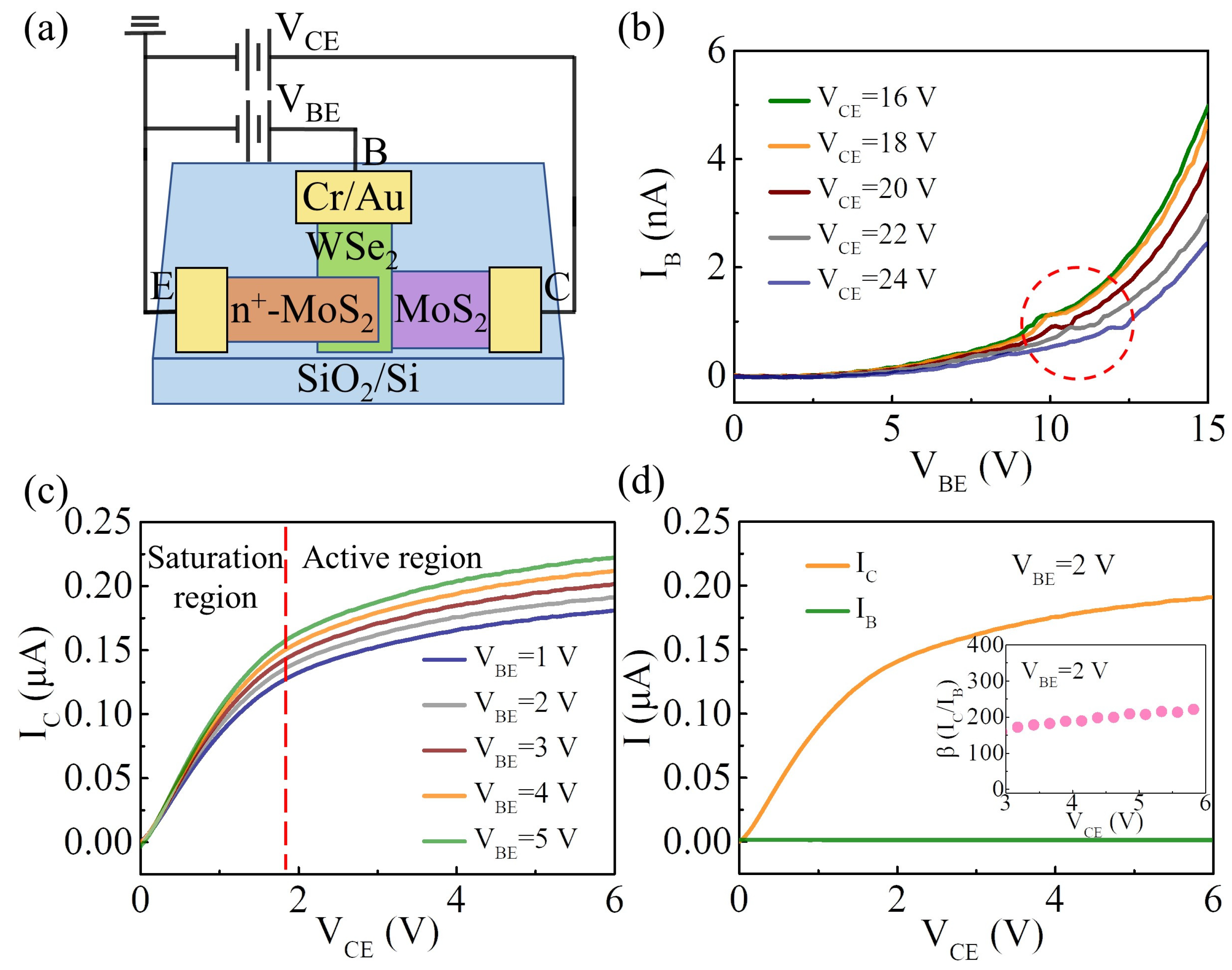
Then the performance of the vertically stacked n+-MoS2/WSe2/MoS2 BJT was investigated under a common-emitter configuration. Figure 4a shows the schematic illustration of the electrical connection. Figure 4b shows the input characteristics of the device, where the I–V curves of the base current (IB) versus VBE at various fixed collector-emitter voltages (VCE) are performed. As the VBE increases, the base current increases exponentially. Additionally, room-temperature NDR effects are observed in Figure 4b (red circle). As the VBE increases, IB initially increases but then decreases and finally gains a second increase in voltage, resulting in a negative slope on the current–voltage curve. This phenomenon may be attributed to lateral band-to-band tunneling, which is consistent with the previously reported performance of MoS2/WSe2 heterojunction [31]. The corresponding band diagram is shown in Figure S5 of the Supplementary Materials. Figure 4c shows the dependence of VCE on the collector current (IC) under several fixed VBE values, which is called the output characteristic of the device. At a small value of VCE (VCE < 1.8 V), the collector current increases approximately linearly with VCE, which is defined as the saturation mode of the BJT. Above the saturation region, IC is mainly dependent on VBE, indicating that the van der Waals BJT is operating in the active region. The difference between IB and IC with a fixed VBE of 2 V is illustrated in Figure 4d. For a BJT operating under the common-emitter configuration, the current gain (β) can be calculated by taking the ratio of IC and IB [32]. A maximum common-emitter current gain of approximately 225 is obtained at VCE = 6 V. The performance of the n-p-n BJTs fabricated by 2D materials is compared and listed in Table 1 [16,22,33,34,35]. Our van der Waals BJT exhibits a relatively high common-emitter current gain.
Furthermore, based on the prepared van der Waals BJT with excellent characteristics, the breakdown characteristics of the device were investigated. Figure 5a shows the open-emitter base-collector breakdown characteristics of the device at room temperature. In this case, the collector was set to ground, a reverse bias was applied to the base-collector junction, and the emitter electrode was set to an open state. At a reverse bias of <25 V, only a small reverse dark current of around 0.14 nA exists. As the reverse bias is increased beyond 25 V, a breakdown occurs, leading to a rapid increase in ICBO. The critical voltage (Vcr) is determined to be 25 V (the gray line) when the dark current begins to increase rapidly [36]. The multiplication factor (M) can be calculated by taking the ratio of ICBO and Is, where Is represents the current at 25 V. Measurements of carrier multiplication M in junctions near breakdown lead to the following empirical equation [37]:
where n represents the ionization index and Vb is a fitting parameter. Equation (1) can be rewritten as follows:
suggesting a linear dependence of ln(1−1/M) on ln(V) in the avalanche carrier multiplication effect. Figure 5b shows the relationship between ln(1−1/M) and ln(V), which directly indicates the occurrence of the avalanche breakdown. In addition, the avalanche breakdown voltage is sensitive to the temperature because a higher electric field is needed to compensate for the energy loss due to electron-phonon scattering as the temperature increases [38]. Therefore, a positive temperature coefficient of the breakdown voltage can be observed in the avalanche carrier multiplication effect [39,40]. Figure 5c shows the open-emitter base-collector breakdown characteristics of the device at different temperatures from 280 K to 340 K. The relationship between the BVCBO (defined as the voltage at which an ICBO of 0.1 μA is measured) and temperature is consistent with the theoretical expectation (Figure 5d).
The open-base collector-emitter breakdown characteristics of the vertically stacked n+-MoS2/WSe2/MoS2 BJT under room temperature conditions were also investigated. The I–V curve and the schematic illustration of the electrical connection are shown in Figure 6a. The ICEO increases slowly at first and then rapidly increases when the VCE is beyond Vcr2 (=35 V), indicating that a breakdown occurs in the van der Waals BJT. The open-base collector-emitter breakdown characteristics of the van der Waals BJT at different temperatures from 280 K to 320 K were also investigated, as shown in Figure S6 of the Supplementary Materials. The BVCEO (defined as the voltage at which an ICEO of 5 μA is measured) increases with the operating temperature, indicating a positive temperature coefficient of the breakdown voltage, as shown in Figure 6b.
4. Conclusions
In summary, a vertically stacked n+-MoS2/WSe2/MoS2 BJT was fabricated by a controlled multistep dry transfer process. The electrical characteristics of the device were investigated, which show relatively large current gains (α ≈ 0.98 and β ≈ 225) under common-base and common-emitter configurations. Additionally, to allow safe measurements at practical current densities, the temperature-dependent breakdown characteristics of the van der Waals BJT were investigated. A BVCBO of 52.9 V and a BVCEO of 40.3 V were obtained at room temperature. With the increase in the operating temperature, the breakdown voltage increases. This work provides a promising way to improve the electrical performance of the van der Waals BJT through proper architecture design and systematically demonstrates the temperature-dependence breakdown characteristics of the device, which might be helpful for the applications of the 2D-material-based BJT in the fields of integrated circuits.
Supplementary Materials
The following supporting information can be downloaded at: https://www.mdpi.com/article/10.3390/nano14080718/s1, Figure S1: (a) A schematic illustration of the electrical connection to investigate the electrical characteristics of the undoped MoS2 flakes with different thicknesses. (b) Typical I–V curves of the undoped MoS2 flakes with different thicknesses; Figure S2: (a) A schematic illustration of the electrical connection to investigate the electrical characteristics of the re-doped MoS2 flakes with different thicknesses. (b) Typical I–V curves of the re-doped MoS2 flakes with different thicknesses; Figure S3: (a) The transfer curve of the individual n+-MoS2 flake; (b) The transfer curve of the individual WSe2 flake; (c) The transfer curve of the individual MoS2 flake; Figure S4: (a) I–V curves of the base-emitter (top-n+-MoS2/WSe2) junction; (b) I–V curves of the base-collector (bottom-MoS2/WSe2) junction; Figure S5: Band diagram of the n+-MoS2/WSe2/MoS2 bipolar junction transistor operating in the negative differential resistance region; Figure S6: The open-base collector-emitter breakdown characteristics of the device operating at different temperatures (from 280 K to 320 K).
Author Contributions
S.D. and N.X. proposed and supervised the project. Z.Y. carried out the experiments and analyzed the data. Z.Y., N.X. and S.D. discussed and interpreted the results. Z.Y. and S.D. wrote the manuscript. All authors have read and agreed to the published version of the manuscript.
Funding
This research was funded by the National Key Basic Research Program of China (grant Nos. 2019YFA0210200 and 2019YFA0210203), the Science and Technology Department of Guangdong Province, and the Fundamental Research Funds for the Central Universities.
Data Availability Statement
The data presented in this article are available at request from the corresponding author.
Conflicts of Interest
The authors declare no conflicts of interest.
References
- Novoselov, K.S.; Geim, A.K.; Morozov, S.V.; Jiang, D.; Zhang, Y.; Dubonos, S.V.; Grigorieva, I.V.; Firsov, A.A. Electric field effect in atomically thin carbon films. Science 2004, 306, 666–669. [Google Scholar] [CrossRef] [PubMed]
- Chang, C.; Chen, W.; Chen, Y.; Chen, Y.; Chen, Y.; Ding, F.; Fan, C.; Fan Hong, J.; Fan, Z.; Gong, C.; et al. Recent Progress on Two-Dimensional Materials. Acta Phys. Chim. Sin. 2021, 37, 2108017. [Google Scholar] [CrossRef]
- Tan, C.L.; Cao, X.H.; Wu, X.J.; He, Q.Y.; Yang, J.; Zhang, X.; Chen, J.Z.; Zhao, W.; Han, S.K.; Nam, G.H.; et al. Recent Advances in Ultrathin Two-Dimensional Nanomaterials. Chem. Rev. 2017, 117, 6225–6331. [Google Scholar] [CrossRef] [PubMed]
- Zhang, J.; Tan, B.Y.; Zhang, X.; Gao, F.; Hu, Y.X.; Wang, L.F.; Duan, X.M.; Yang, Z.H.; Hu, P. Atomically Thin Hexagonal Boron Nitride and Its Heterostructures. Adv. Mater. 2021, 33, 2000769. [Google Scholar] [CrossRef] [PubMed]
- Bian, R.J.; Li, C.C.; Liu, Q.; Cao, G.M.; Fu, Q.D.; Meng, P.; Zhou, J.D.; Liu, F.C.; Liu, Z. Recent progress in the synthesis of novel two-dimensional van der Waals materials. Natl. Sci. Rev. 2022, 9, nwab164. [Google Scholar] [CrossRef] [PubMed]
- Tian, Y.; Zeng, X.J.; Xing, Y.; Chen, J.; Deng, S.Z.; She, J.C.; Liu, F. High-Performance Planar Field-Emission Photodetector of Monolayer Tungsten Disulfide with Microtips. Small 2023, 19, 2304233. [Google Scholar] [CrossRef] [PubMed]
- Liu, Y.; Weiss, N.O.; Duan, X.D.; Cheng, H.C.; Huang, Y.; Duan, X.F. Van der Waals heterostructures and devices. Nat. Rev. Mater. 2016, 1, 16042. [Google Scholar] [CrossRef]
- Castellanos-Gomez, A.; Duan, X.F.; Fei, Z.; Gutierrez, H.R.; Huang, Y.; Huang, X.Y.; Quereda, J.; Qian, Q.; Sutter, E.; Sutter, P. Van der Waals heterostructures. Nat. Rev. Methods Primers 2022, 2, 58. [Google Scholar] [CrossRef]
- Massicotte, M.; Schmidt, P.; Vialla, F.; Schädler, K.G.; Reserbat-Plantey, A.; Watanabe, K.; Taniguchi, T.; Tielrooij, K.J.; Koppens, F.H.L. Picosecond photoresponse in van der Waals heterostructures. Nat. Nanotechnol. 2016, 11, 42–46. [Google Scholar] [CrossRef]
- Tian, Y.; Guo, Z.; Liu, Z.; Lin, H.; Li, X.; Chen, J.; Deng, S.; Liu, F. Efficiently enhanced the visible-light absorption of monolayer WS2 by constructing an asymmetric Fabry-Perot cavity. Mater. Today Nano 2021, 14, 100112. [Google Scholar] [CrossRef]
- Dastgeer, G.; Nisar, S.; Rasheed, A.; Akbar, K.; Chavan, V.D.; Kim, D.K.; Wabaidur, S.M.; Zulfiqar, M.W.; Eom, J. Atomically engineered, high-speed non-volatile flash memory device exhibiting multibit data storage operations. Nano Energy 2024, 119, 109106. [Google Scholar] [CrossRef]
- Dastgeer, G.; Afzal, A.M.; Aziz, J.; Hussain, S.; Jaffery, S.H.A.; Kim, D.K.; Imran, M.; Assiri, M.A. Flexible Memory Device Composed of Metal-Oxide and Two-Dimensional Material (SnO2/WTe2) Exhibiting Stable Resistive Switching. Materials 2021, 14, 7535. [Google Scholar] [CrossRef] [PubMed]
- Nisar, S.; Basha, B.; Dastgeer, G.; Shahzad, Z.M.; Kim, H.; Rabani, I.; Rasheed, A.; Al-Buriahi, M.S.; Irfan, A.; Eom, J.; et al. A Novel Biosensing Approach: Improving SnS2 FET Sensitivity with a Tailored Supporter Molecule and Custom Substrate. Adv. Sci. 2023, 10, 2303654. [Google Scholar] [CrossRef] [PubMed]
- Kim, Y.; Lee, S.; Song, J.G.; Ko, K.Y.; Woo, W.J.; Lee, S.W.; Park, M.; Lee, H.; Lee, Z.; Choi, H.; et al. 2D Transition Metal Dichalcogenide Heterostructures for p- and n-Type Photovoltaic Self-Powered Gas Sensor. Adv. Funct. Mater. 2020, 30, 2003360. [Google Scholar] [CrossRef]
- He, C.L.; Tang, J.; Shang, D.S.; Tang, J.S.; Xi, Y.; Wang, S.P.; Li, N.; Zhang, Q.T.; Lu, J.K.; Wei, Z.; et al. Artificial Synapse Based on van der Waals Heterostructures with Tunable Synaptic Functions for Neuromorphic Computing. ACS Appl. Mater. Interfaces 2020, 12, 11945–11954. [Google Scholar] [CrossRef]
- Su, B.W.; Zhang, X.L.; Yao, B.W.; Guo, H.W.; Li, D.K.; Chen, X.D.; Liu, Z.B.; Tian, J.G. Laser Writable Multifunctional van der Waals Heterostructures. Small 2020, 16, 2003593. [Google Scholar] [CrossRef] [PubMed]
- Liu, L.W.; Xu, N.S.; Ke, Y.L.; Chen, H.J.; Zhang, Y.; Deng, S.Z. Sensing by Surface Work Function Modulation: High Performance Gas Sensing using van der Waals Stacked Bipolar Junction Transistor. Sens. Actuators B Chem. 2021, 345, 130340. [Google Scholar] [CrossRef]
- Lee, G.; Pearton, S.J.; Ren, F.; Kim, J. Two-Dimensionally Layered p-Black Phosphorus/n-MoS2/p-Black Phosphorus Heterojunctions. ACS Appl. Mater. Interfaces 2018, 10, 10347–10352. [Google Scholar] [CrossRef] [PubMed]
- Su, B.W.; Yao, B.W.; Zhang, X.L.; Huang, K.X.; Li, D.K.; Guo, H.W.; Li, X.K.; Chen, X.D.; Liu, Z.B.; Tian, J.G. A gate-tunable symmetric bipolar junction transistor fabricated via femtosecond laser processing. Nanoscale Adv. 2020, 2, 1733–1740. [Google Scholar] [CrossRef] [PubMed]
- Li, H.; Ye, L.; Xu, J.B. High-Performance Broadband Floating-Base Bipolar Phototransistor Based on WSe2/BP/MoS2 Heterostructure. ACS Photonics 2017, 4, 823–829. [Google Scholar] [CrossRef]
- Luo, Z.T.; Yang, M.M.; Wu, D.S.; Huang, Z.H.; Gao, W.; Zhang, M.L.; Zhou, Y.C.; Zhao, Y.; Zheng, Z.Q.; Li, J.B. Rational Design of WSe2/WS2/WSe2 Dual Junction Phototransistor Incorporating High Responsivity and Detectivity. Small Methods 2022, 6, 2200583. [Google Scholar] [CrossRef] [PubMed]
- Dastgeer, G.; Shahzad, Z.M.; Chae, H.; Kim, Y.H.; Ko, B.M.; Eom, J. Bipolar Junction Transistor Exhibiting Excellent Output Characteristics with a Prompt Response against the Selective Protein. Adv. Funct. Mater. 2022, 32, 2204781. [Google Scholar] [CrossRef]
- Shahidul Hassan, M.M.; Domingos, H. Breakdown voltages of base-collector junctions of medium- and low-voltage graded collector transistors. Int. J. Electron. 1991, 70, 69–75. [Google Scholar] [CrossRef]
- Yuan, J.S. Collector-base junction capacitance of advanced bipolar transistors operating at avalanche breakdown. Phys. Status Solidi A 1992, 134, 575–581. [Google Scholar] [CrossRef]
- Maity, S.; Sarkar, K.; Kumar, P. Layered Heterostructures Based on MoS2/MoSe2 Nanosheets Deposited on GaN Substrates for Photodetector Applications. ACS Appl. Nano Mater. 2023, 6, 4224–4235. [Google Scholar] [CrossRef]
- Zhao, W.J.; Ghorannevis, Z.; Amara, K.K.; Pang, J.R.; Toh, M.; Zhang, X.; Kloc, C.; Tan, P.H.; Eda, G. Lattice dynamics in mono- and few-layer sheets of WS2 and WSe2. Nanoscale 2013, 5, 9677–9683. [Google Scholar] [CrossRef] [PubMed]
- Xiao, J.W.; Zhang, Y.; Chen, H.J.; Xu, N.S.; Deng, S.Z. Enhanced Performance of a Monolayer MoS2/WSe2 Heterojunction as a Photoelectrochemical Cathode. Nano-Micro Lett. 2018, 10, 60. [Google Scholar] [CrossRef] [PubMed]
- Kim, J.; Cho, K.; Pak, J.; Lee, W.; Seo, J.; Kim, J.K.; Shin, J.; Jang, J.; Baek, K.Y.; Lee, J.; et al. Channel-Length-Modulated Avalanche Multiplication in Ambipolar WSe2 Field-Effect Transistors. ACS Nano 2022, 16, 5376–5383. [Google Scholar] [CrossRef]
- Luo, P.; Wang, F.K.; Qu, J.Y.; Liu, K.L.; Hu, X.Z.; Liu, K.W.; Zhai, T.Y. Self-Driven WSe2/Bi2O2Se Van der Waals Heterostructure Photodetectors with High Light On/Off Ratio and Fast Response. Adv. Funct. Mater. 2021, 31, 2008351. [Google Scholar] [CrossRef]
- Zhu, J.Q.; Yue, X.F.; Chen, J.J.; Wang, J.; Wan, J.; Bao, W.Z.; Hu, L.G.; Liu, R.; Cong, C.X.; Qiu, Z.J. Ultrasensitive Phototransistor Based on Laser-Induced P-Type Doped WSe2/MoS2 Van der Waals Heterojunction. Appl. Sci. 2023, 13, 6024. [Google Scholar] [CrossRef]
- Nourbakhsh, A.; Zubair, A.; Dresselhaus, M.S.; Palacios, T. Transport Properties of a MoS2/WSe2 Heterojunction Transistor and Its Potential for Application. Nano Lett. 2016, 16, 1359–1366. [Google Scholar] [CrossRef] [PubMed]
- Yan, X.; Zhang, D.W.; Liu, C.S.; Bao, W.Z.; Wang, S.Y.; Ding, S.J.; Zheng, G.F.; Zhou, P. High Performance Amplifier Element Realization via MoS2/GaTe Heterostructures. Adv. Sci. 2018, 5, 1700830. [Google Scholar] [CrossRef] [PubMed]
- Lin, C.Y.; Zhu, X.D.; Tsai, S.H.; Tsai, S.P.; Lei, S.D.; Shi, Y.M.; Li, L.J.; Huang, S.J.; Wu, W.F.; Yeh, W.K.; et al. Atomic-Monolayer Two-Dimensional Lateral Quasi-Heterojunction Bipolar Transistors with Resonant Tunneling Phenomenon. ACS Nano 2017, 11, 11015–11023. [Google Scholar] [CrossRef] [PubMed]
- Liu, L.W.; Xu, N.S.; Zhang, Y.; Zhao, P.; Chen, H.J.; Deng, S.Z. Van der Waals Bipolar Junction Transistor Using Vertically Stacked Two-Dimensional Atomic Crystals. Adv. Funct. Mater. 2019, 29, 1807893. [Google Scholar] [CrossRef]
- Afzal, A.M.; Iqbal, M.Z.; Dastgeer, G.; Nazir, G.; Mumtaz, S.; Usman, M.; Eom, J. WS2/GeSe/WS2 Bipolar Transistor-Based Chemical Sensor with Fast Response and Recovery Times. ACS Appl. Mater. Interfaces 2020, 12, 39524–39532. [Google Scholar] [CrossRef] [PubMed]
- Son, B.; Wang, Y.D.; Luo, M.L.; Lu, K.Z.; Kim, Y.; Joo, H.J.; Yi, Y.; Wang, C.W.; Wang, Q.J.; Chae, S.H.; et al. Efficient Avalanche Photodiodes with a WSe2/MoS2 Heterostructure via Two-Photon Absorption. Nano Lett. 2022, 22, 9516–9522. [Google Scholar] [CrossRef] [PubMed]
- Ouyang, T.H.; Wang, X.M.; Liu, S.J.; Chen, H.J.; Deng, S.Z. A Complete Two-Dimensional Avalanche Photodiode Based on MoTe2-WS2-MoTe2 Heterojunctions with Ultralow Dark Current. Front. Mater. 2021, 8, 736180. [Google Scholar] [CrossRef]
- Pak, J.; Jang, Y.; Byun, J.; Cho, K.; Kim, T.Y.; Kim, J.K.; Choi, B.Y.; Shin, J.; Hong, Y.; Chung, S.; et al. Two-Dimensional Thickness-Dependent Avalanche Breakdown Phenomena in MoS2 Field-Effect Transistors under High Electric Fields. ACS Nano 2018, 12, 7109–7116. [Google Scholar] [CrossRef] [PubMed]
- Lan, C.Y.; Li, C.; Wang, S.; He, T.Y.; Jiao, T.P.; Wei, D.P.; Jing, W.K.; Li, L.Y.; Liu, Y. Zener Tunneling and Photoresponse of a WS2/Si van der Waals Heterojunction. ACS Appl. Mater. Interfaces 2016, 8, 18375–18382. [Google Scholar] [CrossRef] [PubMed]
- Dastgeer, G.; Khan, M.F.; Nazir, G.; Afzal, A.M.; Aftab, S.; Naqvi, B.A.; Cha, J.; Min, K.A.; Jami, Y.; Jung, J.; et al. Temperature-Dependent and Gate-Tunable Rectification in a Black Phosphorus/WS2 van der Waals Heterojunction Diode. ACS Appl. Mater. Interfaces 2018, 10, 13150–13157. [Google Scholar] [CrossRef] [PubMed]
Figure 1.
The schematic illustration and the optical microscopy images show the fabrication procedure of the vertically stacked n+-MoS2/WSe2/MoS2 BJT. (a) Bottom multilayer MoS2; (b) MoS2/WSe2 n-p heterostructure; (c) vertically stacked n+-MoS2/WSe2/MoS2 heterostructure; (d) Cr/Au metal electrodes connected to the heterostructure.

Figure 2.
(a) Raman spectra of bottom MoS2 (blue line), WSe2 (brown line), top n+-MoS2 (orange line), and WSe2/MoS2 heterostructure (green line); (b) the AFM height profile of the BJT.
Figure 2.
(a) Raman spectra of bottom MoS2 (blue line), WSe2 (brown line), top n+-MoS2 (orange line), and WSe2/MoS2 heterostructure (green line); (b) the AFM height profile of the BJT.

Figure 3.
(a) Schematic illustration to show the electric connection of the device under the common-base configuration; (b) input characteristics of the device under the common-base configuration; (c) output characteristics of the device under the common-base configuration; (d) IE (green curve), IC (yellow curve), and α (pink dotted line) are shown as a function of VBE at VCB = 5 V.

Figure 4.
(a) A schematic illustration to show the electric connection of the device under the common-emitter configuration; (b) input characteristics of the device under the common-emitter configuration. The inset of the red circle shows the NDR effect region; (c) output characteristics of the device under the common-emitter configuration; (d) IC (yellow curve) and IB (green curve) are shown as a function of VCE at VBE = 2 V. The inset shows the calculated common-emitter current gain (β = IC/IB) as a function of VCE at VBE = 2 V.

Figure 5.
(a) I–V curve for the open-emitter base-collector junction showing the avalanche effect at a large reverse bias beyond Vcr. The inset shows a schematic illustration of the electric connection; (b) logarithmic plot of 1−1/M versus V. n represents the ionization index, obtained by the linear fitting of the plot near ln(Vcr); (c) I–V curve for the open-emitter base-collector junction at different temperatures (from 280 K to 340 K); (d) the BVCBO as a function of temperature.

Figure 6.
(a) The open-base collector-emitter breakdown characteristics of the van der Waals BJT at room temperature. The inset shows the schematic illustration of the electric connection; (b) the BVCEO as a function of temperature.
Figure 6.
(a) The open-base collector-emitter breakdown characteristics of the van der Waals BJT at room temperature. The inset shows the schematic illustration of the electric connection; (b) the BVCEO as a function of temperature.


Table 1.
Summary of the performance of this work and recently reported BJT prepared by 2D materials [16,22,33,34,35].
| Material | Structure | Type | α | β | Ref. |
|---|---|---|---|---|---|
| n+-MoS2/WSe2/MoS2 | Vertical | npn | 0.98 | 225 | This work |
| MoTe2/GeSe/MoTe2 | Vertical | npn | 0.95 | 29.3 | [22] |
| MoS2/WSe2/MoS2 | Vertical | npn | 0.97 | 12 | [34] |
| WS2/GeSe/WS2 | Vertical | npn | 1.11 | 20.7 | [35] |
| MoS2/WSe2/MoS2 | Lateral | npn | / | 3 | [33] |
| MoS2/BP/MoS2 | Lateral | npn | 0.98 | 41 | [16] |
Disclaimer/Publisher’s Note: The statements, opinions and data contained in all publications are solely those of the individual author(s) and contributor(s) and not of MDPI and/or the editor(s). MDPI and/or the editor(s) disclaim responsibility for any injury to people or property resulting from any ideas, methods, instructions or products referred to in the content. |
© 2024 by the authors. Licensee MDPI, Basel, Switzerland. This article is an open access article distributed under the terms and conditions of the Creative Commons Attribution (CC BY) license (https://creativecommons.org/licenses/by/4.0/).
Share and Cite
MDPI and ACS Style
Yan, Z.; Xu, N.; Deng, S. Realization of High Current Gain for Van der Waals MoS2/WSe2/MoS2 Bipolar Junction Transistor. Nanomaterials 2024, 14, 718. https://doi.org/10.3390/nano14080718
AMA Style
Yan Z, Xu N, Deng S. Realization of High Current Gain for Van der Waals MoS2/WSe2/MoS2 Bipolar Junction Transistor. Nanomaterials. 2024; 14(8):718. https://doi.org/10.3390/nano14080718
Chicago/Turabian StyleYan, Zezhang, Ningsheng Xu, and Shaozhi Deng. 2024. "Realization of High Current Gain for Van der Waals MoS2/WSe2/MoS2 Bipolar Junction Transistor" Nanomaterials 14, no. 8: 718. https://doi.org/10.3390/nano14080718
Note that from the first issue of 2016, this journal uses article numbers instead of page numbers. See further details here.