High-Aspect Ratio β-Ga2O3 Nanorods via Hydrothermal Synthesis
by

Hyun Jeong Bae
1, 
Tae Hee Yoo
1,
Youngbin Yoon
1,
In Gyu Lee
1,
Jong Pil Kim
2,
Byung Jin Cho
3 and
Wan Sik Hwang
1,* 1
Department of Materials Engineering, Korea Aerospace University, Goyang 10540, Korea
2
Division of Analysis & Research, Korea Basic Science Institute, Busan 46742, Korea
3
School of Electrical Engineering, KAIST, Daejeon 34141, Korea
*
Author to whom correspondence should be addressed.
Nanomaterials 2018, 8(8), 594; https://doi.org/10.3390/nano8080594
Submission received: 28 June 2018
/
Revised: 2 August 2018
/
Accepted: 2 August 2018
/
Published: 5 August 2018
Abstract
:High-aspect ratio β-Ga2O3 nanorods consisting of prism-like crystals were formed using gallium oxyhydroxide and ammonia hydroxide via a hydrothermal synthesis followed by the subsequent calcination process. The formation of high-aspect ratio β-Ga2O3 nanorods was attributed to the oriented attachment mechanism that was present during the hydrothermal synthesis. A field-effect transistor was fabricated using the high-aspect ratio β-Ga2O3 nanorod, and it exhibited the typical charge transfer properties of an n-type semiconductor. This facile approach to forming high-aspect ratio nanorods without any surfactants or additives can broaden the science of β-Ga2O3 and expedite the integration of one-dimensional β-Ga2O3 into future electronics, sensors, and optoelectronics.
1. Introduction
Gallium oxide in general and β-Ga2O3 in particular are getting more attention as exciting wide bandgap and nearly direct bandgap semiconductors (WBSes) [1,2,3,4]. The research and development around the Ga2O3-based semiconductor has offered substantial benefits to areas such as power electronics, high-speed electronics, photoelectrochemistry, photocatalysis, and gas/photon sensors [5,6]. Like other semiconductors, the low-dimensional properties of β-Ga2O3 have broadened the science of the materials, eventually leading to the promotion of innovative technologies, which have in turn promoted the development of new materials [7,8,9,10]. Numerous studies have been conducted on the synthesis and characterization of one-dimensional (1D) and two-dimensional (2D) β-Ga2O3 [11,12,13] mainly via chemical reaction-based approaches such as hydrolysis, sol–gel methods, electrospinning, and the hydrothermal method [14,15,16,17,18,19,20]. Among these various methods, β-Ga2O3 prepared via the hydrothermal method has been popular due to the resulting high crystallinity [21,22,23,24,25,26]. Furthermore, the hydrothermal method allows the formed β-Ga2O3 to have different faces of nanorods and/or nanoparticles, resulting in different surface area to volume ratios and/or aspect ratios. In fact, a minor change in aspect ratio can substantially change the optical, biological, and electrical properties. To elongate a certain desired direction, Ga2O3 nanorods are often synthesized via the catalytic chemical vapor deposition method and laser ablation, which requires elevated temperature reactions [27,28]. On the other hand, template-assisted and surfactant-assisted hydrothermal methods have also been developed to form Ga2O3 nanorods [28,29,30,31]. However, these methods bring up additional issues such as cross-contamination, unintentional doping, and increases in product costs [24,32]. In this study, a simple and facile method is introduced to form high-aspect ratio nanorods without any surfactants or additives, which can broaden the science of β-Ga2O3 and expedite the integration of 1D β-Ga2O3 into future electronics, sensors, and optoelectronics
2. Experimental
2.1. Precipitated α-GaOOH, Hydrothermal-Synthesized α-GaOOH, and β-Ga2O3 Nanorods
0.1 M Gallium(III) nitrate hydrate (Ga(NO3)3∙xH2O) was dissolved in 50 mL of deionized (DI) water via magnetic stirring at room temperature. The resultant solution was clear with a pH of 2.5. The solution was mixed with an ammonium hydroxide solution (from 28 to 30% NH3 in solution) on a hot plate at 60 °C to reach pH 10; the pH value changed in the range between 10.2 and 10.0 depending on the aging time. The supersaturated solution was subsequently aged from 10 min to 6 h in the beaker with magnetic stirring at 60 °C; there were no changes in process conditions other than the aging time. Next, at different aging times, the solution was transferred to a Teflon-lined stainless-steel autoclave that was sealed and heated in an electric oven at 140 °C for 10 h. (This method is known as hydrothermal synthesis). The autoclave was then naturally cooled down to room temperature. Finally, α-GaOOH was collected and washed several times with DI water to remove the residual reagents and dried in an oven at 70 °C for 6 h. The α-GaOOH nanorods turned into β-Ga2O3 nanorods after an annealing process at 1000 °C for 5 h. (This method is known as the calcination process).
2.2. Material Characterization
The morphologies and sizes of the α-GaOOH and β-Ga2O3 nanorods at different aging times were characterized using a field-emission scanning electron microscope (FESEM, JSM-7100F, JEOL, Peabody, MA, USA). The structure and crystallinity of the nanorods were examined using powder X-ray diffraction (XRD, SMARTLAB, RIGAKU, Tokyo, Japan) with Cu Kα radiation (λ = 0.154 nm) and high-resolution transmission electron microscopy (HRTEM, JEM 2100F, JEOL, Peabody, MA, USA; point resolution: 0.24 nm, lattice resolution: 0.1 nm) operating at an acceleration voltage of 200 kV. A Fourier transform infrared (FTIR, CARY670, Agilent, Santa Clara, CA, USA) spectrometer was also employed to analyze the chemical bonding of the α-GaOOH and β-Ga2O3 in the wavenumber range of 4000–450 cm−1.
2.3. Fabrication of the Ga2O3 Nanorods Field-Effect Transistor (FET)
The high-aspect ratios β-Ga2O3 nanorods were mechanically transferred onto the back-gated SiO2/p+ Si (300 nm/500 mm) substrate. The 10-μm spaced source/drain contacts (100 μm × 100 μm) were patterned on top of β-Ga2O3 nanorods using a conventional photolithography process followed by lift-off processes. Ti (5 nm) and TiN (500 nm) were deposited via physical vapor deposition for the metal contacts. Before electrical measurements, the devices underwent an annealing process at 300 °C for 3 h to improve their contact resistance. Electrical characterizations were performed using current-voltage measurements (Keithley 4200A-SCS, Tektronix, Beaverton, OR, USA) at room temperature.
3. Results and Discussion
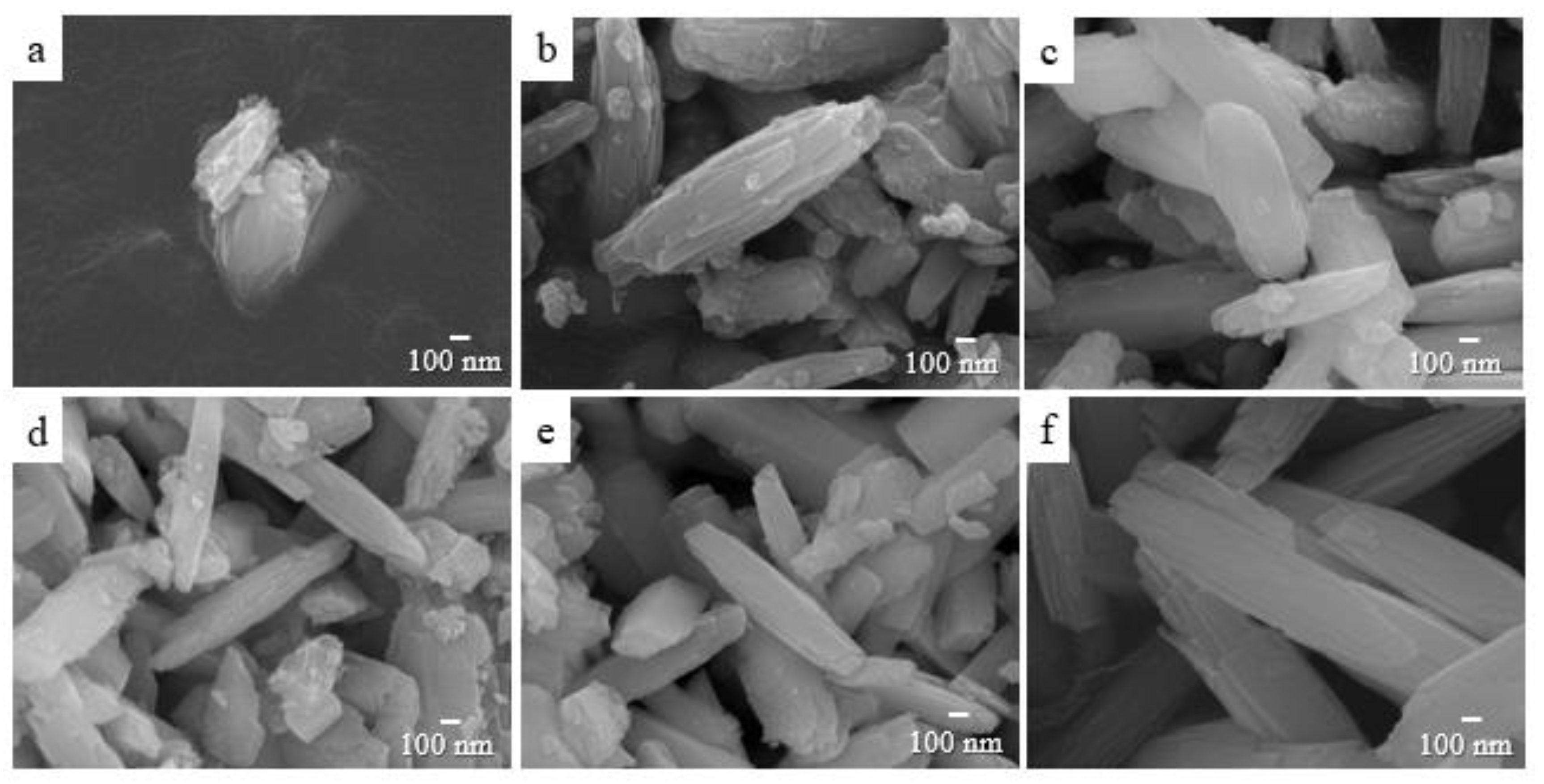
Figure 1 shows the FESEM images of the precipitated nanostructures obtained from the supersaturated solution at different aging times. In the presence of alkali, the α-GaOOH nanoparticles precipitated immediately due to the reaction between the hydrated gallium as Ga(OH)3 and ammonium hydroxide in the supersaturated condition [33,34]. The unstable nanoparticles were subsequently aggregated by the well-known van der Waals force to form bigger nanoparticles [35]. Under this condition, the α-GaOOH nanoparticles selectively absorbed OH− ions on all specific surfaces and formed a primary nanoplate along the preferential direction with a lower surface energy [30,33]. Aiding in lowering the surface energy, this primary nanoplate aggregated to form a stacked anisotropic nanoplatelet with a face-to-face plane that finally formed spindle-like α-GaOOH nanorods via the growth mechanism known as Ostwald ripening and oriented attachment [36]. The aggregated nanostructure at the aging time of 10 min (Figure 1a) turned out to be amorphous according to the XRD. As the aging time increased, aside from small nanoparticles, well-defined prismatic nanorods with specific facets (spindle-like nanorods) appeared at 1 h of aging, as shown in Figure 1b. The FESEM image showed that these spindle-like nanorods were composed of face-to-face stacked anisotropic nanoplatelets. In other words, the nanoplates, aggregating with the face-to-face plane to reduce the surface energy of the primary nanoplates, eventually formed spindle-like nanorods [33,37,38]. As the aging time increased further, the spindle-like nanorods dominated uniformly at the expense of the small nanoparticles, and eventually prism-like nanorods dominated without small nanoparticles after 6 h of aging. The above observation presumably suggested that the face-to-face stacked anisotropic nanoplatelets assembled the spindle-like nanorods.
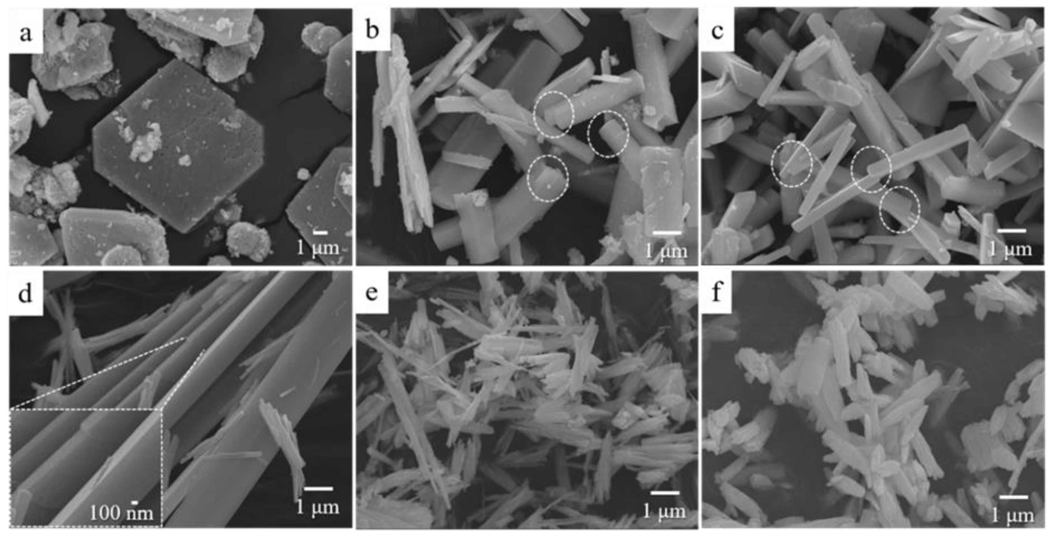
Figure 2 shows the FESEM images of the various β-Ga2O3 nanorods that aged from 10 min to 6 h, followed by the identical hydrothermal and calcination processes. The FESEM images of the hydrothermal-synthesized α-GaOOH nanorods before the calcination process are not shown in this work because no notable differences were observed between the hydrothermal-synthesized α-GaOOH nanorods and calcinated β-Ga2O3 nanorods via FESEM. Nevertheless, the thermogravimetry (TGA) and differential scanning calorimeter (DSC) analysis revealed that this phase transformation was accompanied by a 2–8.8% weight loss [39,40]. For the 10-min aging condition, diverse morphologies of 3D flower-like and 2D sheet-like nanostructures as well as small nanoparticles were observed, as shown in Figure 2a, while nanorod structures appeared at aging times in the range from 1 h to 6 h, as shown in Figure 2b–f. A detailed discussion on these differences is outside the scope in this work; focus is centered on the formation of the high-aspect-ratio nanorods. Figure 2b showed that the products obtained after 1 h of aging followed by hydrothermal and calcination processes were comprised of prism-like nanorods and spindle-like nanorods as well as nanoparticles. As the aging time increased further, the prism-like nanorods with smooth surfaces (Figure 2b,c) turned into bundles of small nanorods with split structures (Figure 2e,f)). The edges of the split structure became grounded while the size of the nanorods remained unchanged at 6 h of aging, as shown in Figure 2f. It was interesting to notice that there was a transition condition where both the prism-like nanorods and nanorod bundles with split structures coexisted. The formed prism-like nanorods at this transition condition (Figure 2d) showed an extremely high aspect ratio without any surfactants or additives involved.
The comparison between Figure 1 and Figure 2 revealed that the lengths of the β-Ga2O3 nanorods (Figure 2) were longer than those of the precipitated α-GaOOH nanorods (Figure 1). Furthermore, the results showed that the morphology changes of the precipitated α-GaOOH nanorods depending on the different aging times (Figure 1) were insignificant, while the morphology changes of the hydrothermal-synthesized α-GaOOH nanorods (Figure 2) were significant. This implied that the precipitated products played a very important role for the diverse morphologies of the hydrothermal-synthesized products.
Figure 3a,b show the TEM images of the typical high-aspect ratio β-Ga2O3 nanorods. While the reported high-aspect ratio GaOOH was in tube (hollow cylinder) form [41], the high-aspect ratio β-Ga2O3 in this work was in nanorod form. The electron diffraction pattern of the selected area is shown in Figure 3c, and the atomic-scale image in Figure 3d is the Fourier transform of the the diffraction pattern. The results revealed that the formed high-aspect ratio β-Ga2O3 possessed excellent crystallinity with an interplanar spacing of about 0.267 nm, which corresponded to the ( 1 1-) crystal plane of monoclinic Ga2O3. Other than the high-aspect ratio β-Ga2O3, conventional β-Ga2O3 nanorods were also crystalized, as shown in Figure 3e.
The crystallinity of the obtained nanostructures was further characterized using an XRD analysis, as shown in Figure 4a. The X-ray diffraction patterns of the precipitated and the hydrothermal-synthesized α-GaOOH nanorod with 2 h of aging were perfectly indexed to the orthorhombic α-GaOOH phase with the following cell constants: a = 4.58 Å, b = 9.80 Å, c = 2.97 Å. This agrees well with the literature (JCPDS card No. 06-0180). In detail, the intensity of the hydrothermal-synthesized α-GaOOH nanorods was much sharper and stronger than that of the precipitated α-GaOOH nanorods. This indicated that the precipitated nanorods retained their orthorhombic α-GaOOH structures even after the hydrothermal process, and the hydrothermal process enhanced the crystal growth and the crystallinity of the α-GaOOH nanorods. The hydrothermal-synthesized α-GaOOH transformed into the monoclinic β-Ga2O3 nanorods (JCPDS card No. 76-0573) via the calcination at 1000 °C for 5 h, as shown in Figure 4a. It was noted that the 10-min aged products were found to be amorphous because no obvious diffraction peaks were observed via XRD. It took around 1 h of aging for the amorphous nanoparticles to aggregate with each other to form specific facets.
The chemical structures of the nanorods were also characterized using FTIR spectroscopy in the range from 4000 to 450 cm−1 regions. Figure 4b shows the chemical structures of the precipitated α-GaOOH nanorods, the hydrothermal-synthesized α-GaOOH nanorods, and β-Ga2O3 nanorods with 2 h of aging. The broad bands at around 3457 cm−1 and 1630 cm−1 from the precipitated α-GaOOH nanorods with 2 h of aging represented the stretching vibration of the H–O–H and O–H bonds, respectively [42,43]. This indicated that water molecules remained in the precipitated α-GaOOH nanorods [44]. Other than the water molecule-related peaks, the strong bending vibrations at 1019 and 945 cm−1 were attributed to the Ga–OH bands in the α-GaOOH nanorods [26,34]. The strong bands at 649 cm−1 and 477 cm−1 represented the Ga–O bending vibration and Ga–O stretching vibration [45], respectively. After the hydrothermal and further calcination process, the peaks representing the Ga-related peaks enhanced while the water molecule-related peaks diminished.
A length distribution histogram of the β-Ga2O3 nanorods obtained at different aging times is shown in Figure 5a, which was extracted from the SEM images by considering 100 nanostructures. The result revealed two key features: (i) regardless of the different aging times (except 2 and 2.5 h of aging), the mean length of the final β-Ga2O3 nanorods remained around 3 μm with a gaussian normal distribution; (ii) on the contrary, the size distribution of the β-Ga2O3 nanorods at 2 h and 2.5 h of aging became uneven. This indicated that chemical reactions such as nucleation, growth and dissolution, and re-growth et al. played a significant role for all conditions other than 2 and 2.5 h of aging, because these times showed gaussian normal distributions. Unlike the gaussian normal distribution, the final β-Ga2O3 nanorods at 2 h and 2.5 h of aging showed uneven size distributions. This indicated that aside from the normal chemical reaction, other mechanisms such as oriental attachment were presumably a main driving force in forming the high-aspect ratio β-Ga2O3 nanorods.
It is worthwhile postulating on the growth mechanism of the high-aspect ratio β-Ga2O3 nanorods. It has been reported that the morphology and size of hydrothermal-synthesized α-GaOOH or β-Ga2O3 nanorods can be affected by pH values, hydrothermal synthesis times/temperatures, reaction temperatures, and alkali chemicals [33,34,41,46,47]. We argue that aside from these factors, the aging time used to form the precipitated products in the supersaturated solution could also significantly affect the morphology and size of the α-GaOOH or β-Ga2O3 nanorods. The SEM images in Figure 2b,c revealed that the nanorods with prism-like crystals tended to attach in certain planes because they reduced the total surface energy of the nanoparticles in the solution [47,48]. As the aging time increased, this preferred attachment parallel to the plane could be enhanced, thereby forming high-aspect ratio nanorods, as shown in Figure 2d. The attachment of the nanorods parallel to the plane could be supported via the high-resolution SEM image (inset) in Figure 2d. Based on the hypothesis, the re-attachment in the plane was preferable at 2 h of aging, which eventually caused the high-aspect ratio β-Ga2O3 nanorods with prism-like crystals with an uneven distribution. It was noted that the precipitated nanorods with smooth surfaces in Figure 1 were dissolved and re-assembled continually in the supersaturated solution. Unlike the newly-formed nanorods at shorter aging times, the re-assembled nanorods at longer aging times presumably possessed more defects and mismatches. These accumulated defects and mismatches on surface of the re-assembled nanorods prevented the attachment of nanorods parallel to the plane, causing the crystal to split and leading to bundles of small nanorods of split structures. The overall mechanism is described in Figure 5b.
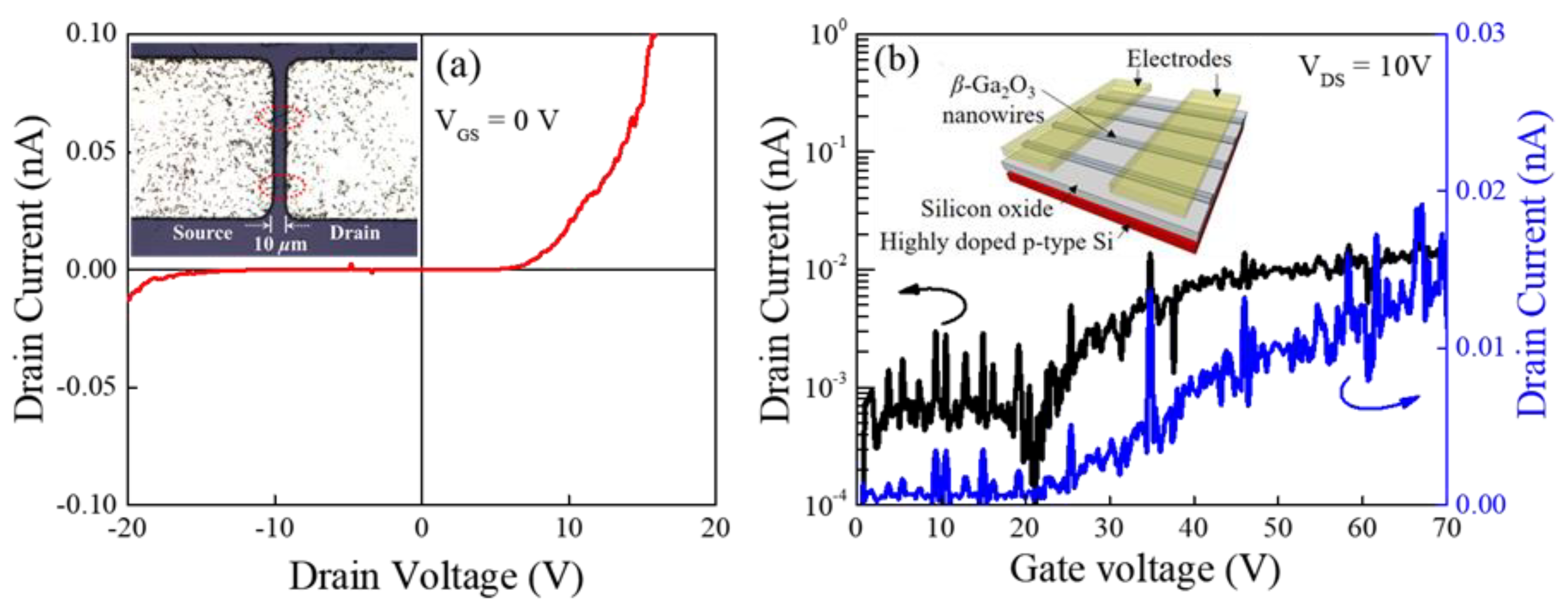
The formed high-aspect ratio β-Ga2O3 nanorods via hydrothermal synthesis followed by the calcination process were transferred into the back-gated SiO2/p+ Si substrate, and then, a conventional lift-off process was performed to fabricate the device, as shown in the inset of Figure 6. Figure 6a,b shows output (IDS-VDS) and transfer (IDS-VGS) characteristics of the Ga2O3 nanorod FETs. Figure 6a showed that at least 10 V was required to overcome the Schottky barrier at the edge of the source-to-channel region. Then the VDS = 10 V was applied to evaluate the transfer curve as shown in Figure 6b. It reveals the typical charge transfer properties of an n-type semiconductor. The gate modulation was not impressive, mainly due to the low on-state current limited by the high contact resistance, which would be improved by adopting a doping technique at the source/drain and channel regions. It was reported that this unintentionally n-type behavior in the undoped β-Ga2O3 was attributed to the the oxygen deficiency and/or residual impurities [49,50].
4. Conclusions
High-aspect ratio β-Ga2O3 nanorods were formed using gallium oxyhydroxide and ammonia hydroxide via a hydrothermal synthesis followed by a subsequent calcination process. The results showed that the morphology changes of the precipitated α-GaOOH nanorods depending on the different aging times were insignificant, while those of the hydrothermal-synthesized α-GaOOH nanorods were significant. This implied that the precipitated products played a very important role in the final products after the hydrothermal process. The formation of the high-aspect ratio β-Ga2O3 nanorods was presumably attributed to the re-attachment of the newly formed nanorodes in the plane of the nanostructures. Furthermore, a field-effect transistor was fabricated using the β-Ga2O3 nanorod, showing the typical charge transfer properties of an n-type semiconductor. This facile approach to forming a high-aspect ratio nanorods without any surfactants or additives can broaden β-Ga2O3 science and expedite the integration of one-dimensional β-Ga2O3 into future electronics, sensors, and optoelectronics.
Author Contributions
Conceptualization, W.S.H.; Formal analysis, I.G.L.; Methodology, J.P.K.; Resources, H.J.B.; T.H.Y. and Y.Y.; Writing—review & editing, B.J.C.
Funding
This work was funded by the Agency for Defense Development (ADD-15-113-205-020), by Basic Science Research Program (2017R1A2B4012278) by the National Research Foundation of Korea (NRF), and by the Center for Advanced Soft-Electronics that is funded by the Ministry of Science, ICT and Future Planning, through the Global Frontier Project (CASE-2011-0031638).
Conflicts of Interest
The authors declare no conflict of interest.
References
- Higashiwaki, M.; Sasaki, K.; Kuramata, A.; Masui, T.; Yamakoshi, S. Depletion-mode Ga2O3 metal-oxide-semiconductor field-effect transistors on β-Ga2O3 (010) substrates and temperature dependence of their device characteristics. Appl. Phys. Lett. 2012, 100, 013504. [Google Scholar] [CrossRef]
- Sasaki, K.; Kuramata, A.; Masui, T.; Víllora, E.G.; Shimamura, K.; Yamakoshi, S. Device-Quality β-Ga2O3 Epitaxial Films Fabricated by Ozone Molecular Beam Epitaxy. Appl. Phys. Exp. 2012, 5, 035502. [Google Scholar] [CrossRef]
- Zhou, H.; Maize, K.; Noh, J.; Shakouri, A.; Ye, P.D. Thermodynamic Studies of β-Ga2O3 Nanomembrane Field-Effect Transistors on a Sapphire Substrate. ACS Omega 2017, 2, 7723–7729. [Google Scholar] [CrossRef]
- Higashiwaki, M.; Sasaki, K.; Murakami, H.; Kumagai, Y.; Koukitu, A.; Kuramata, A.; Masui, T.; Yamakoshi, S. Recent progress in Ga2O3 power devices. Semicond. Sci. Technol. 2016, 31, 034001. [Google Scholar] [CrossRef]
- Li, X.; Zhen, X.; Meng, S.; Xian, J.; Shao, Y.; Fu, X.; Li, D. Structuring β-Ga2O3 Photonic Crystal Photocatalyst for Efficient Degradation of Organic Pollutants. Environ. Sci. Technol. 2013, 47, 9911–9917. [Google Scholar] [CrossRef] [PubMed]
- Liu, Z.; Yamazaki, T.; Shen, Y.; Kikuta, T.; Nakatani, N.; Li, Y. O2 and CO sensing of Ga2O3 multiple nanowire gas sensors. Sens. Actuator B Chem. 2008, 129, 666–670. [Google Scholar] [CrossRef]
- Kim, J.; Mastro, M.A.; Tadjer, M.J.; Kim, J. Quasi-Two-Dimensional h-BN/β-Ga2O3 Heterostructure Metal-Insulator-Semiconductor Field-Effect Transistor. ACS Appl. Mater. Interfaces 2017, 9, 21322–21327. [Google Scholar] [CrossRef] [PubMed]
- Kalygina, V.M.; Zarubin, A.N.; Nayden, Y.P.; Novikov, V.A.; Petrova, Y.S.; Tolbanov, O.P.; Tyazhev, A.V.; Yaskevich, T.M. Ga2O3 Films Formed by Electrochemical Oxidation. Semiconductors 2011, 45, 1097–1102. [Google Scholar] [CrossRef]
- Jangir, R.; Ganguli, T.; Tiwari, P.; Porwal, S.; Srivastava, H.; Rai, S.K.; Khattak, B.Q.; Oak, S.M. Synthesis and characterization of β-Ga2O3 nanostructures grown on GaAs substrates. Appl. Surf. Sci. 2011, 257, 9323–9328. [Google Scholar] [CrossRef]
- Wang, F.; Han, Z.; Tong, L. Fabrication and characterization of β-Ga2O3 optical nanowires. Physica E 2005, 30, 150–154. [Google Scholar] [CrossRef]
- Hwang, W.S.; Verma, A.; Peelaers, H.; Protasenko, V.; Rouvimov, S.; Xing, H.; Seabaugh, A.; Haensch, W.; Walle, C.V.; Galazka, Z.; et al. High-voltage field effect transistors with wide-bandgap β-Ga2O3 nanomembranes. Appl. Phys. Lett. 2014, 104, 203111. [Google Scholar] [CrossRef]
- Kwon, Y.B.; Lee, G.Y.; Oh, S.Y.; Kim, J.H.; Pearton, S.J.; Ren, F. Tuning the thickness of exfoliated quasi-two-dimensional β-Ga2O3 flakes by plasma etching. Appl. Phys. Lett. 2017, 110, 131901. [Google Scholar] [CrossRef]
- Feng, W.; Wang, X.; Zhang, J.; Wang, L.; Zheng, W.; Hu, P.; Cao, W.; Yang, B. Synthesis of two-dimensional β-Ga2O3 nanosheets for high-performance solar blind photodetectors. J. Mater. Chem. C 2014, 2, 3254. [Google Scholar] [CrossRef]
- Yoon, Y.B.; Han, K.I.; Kim, B.H.; Lee, I.G.; Kim, Y.H.; Kim, J.P.; Hwang, W.S. Formation of β-Ga2O3 nanofibers of sub-50 nm diameter synthesized by electrospinning method. Thin Solid Films 2018, 1, 358–362. [Google Scholar] [CrossRef]
- Hailin, M.; Yan, L. One-Step Preparation of β-Ga2O3 Nanomaterial and Research the Electrical Transport Properties at High Temperature. Rare Metal. Mater. Eng. 2013, 42, 2245–2247. [Google Scholar] [CrossRef]
- Khan, A.; Jadwisienczak, W.M.; Kordesch, M.E. One-step preparation of ultra-wide β-Ga2O3 microbelts and their photoluminescence study. Physica E 2006, 35, 207–211. [Google Scholar] [CrossRef]
- Oh, S.Y.; Kim, J.H.; Ren, F.; Peartonc, S.J.; Kim, J.H. Quasi-two-dimensional β-gallium oxide solar-blind photodetectors with ultrahigh responsivity. J. Mater. Chem. C 2016, 4, 9245–9250. [Google Scholar] [CrossRef]
- Reddy, L.S.; Ko, Y.H.; Yu, J.S. Hydrothermal Synthesis and Photocatalytic Property of β-Ga2O3 Nanorods. Nanoscale Res. Lett. 2015, 10, 364. [Google Scholar] [CrossRef] [PubMed]
- Sharma, S.; Sunkara, M.K. Direct Synthesis of Gallium Oxide Tubes, Nanowires, and Nanopaintbrushes. J. Am. Chem. Soc. 2002, 124, 12288–12293. [Google Scholar] [CrossRef] [PubMed]
- Kokubun, Y.; Miura, K.; Endo, F.; Nakagomi, S. Sol-gel prepared β-Ga2O3 thin films for ultraviolet photodetectors. Appl. Phys. Lett. 2007, 90, 031912. [Google Scholar] [CrossRef]
- Kang, B.K.; Mang, S.R.; Song, K.M.; Lee, K.S.; Yoon, D.H. Hydrothermal synthesis and characterization of uniform β-Ga2O3 hollow nanostructures by carbon nanospheres. J. Ceram. Process. Res. 2014, 15, 200–203. [Google Scholar]
- Zhang, J.; Liu, Z.; Lin, C.; Lin, J. A simple method to synthesize β-Ga2O3 nanorods and their photoluminescence properties. J. Cryst. Growth 2005, 280, 99–106. [Google Scholar] [CrossRef]
- EL-Sayed, E.I.; Al-Ghamdi, A.A.; Al-Heniti, S.; Al-Marzouki, F.; El-Tantawy, F. Synthesis of ultrafine β-Ga2O3 nanopowder via hydrothermal approach: A strong UV “excimer-like” emission. Mater. Lett. 2011, 65, 317–321. [Google Scholar] [CrossRef]
- Quan, Y.; Fang, D.; Zhang, X.; Liu, S.; Huang, K. Synthesis and characterization of gallium oxide nanowires via a hydrothermal method. Mater. Chem. Phys. 2010, 121, 142–146. [Google Scholar] [CrossRef]
- Sun, M.; Li, D.; Zhang, W.; Fu, X.; Shao, Y.; Li, W.; Xiao, G.; He, Y. Rapid microwave hydrothermal synthesis of GaOOH nanorods with photocatalytic activity toward aromatic compounds. Nanotechnology 2010, 21, 355601. [Google Scholar] [CrossRef] [PubMed]
- Zhao, Y.; Frost, R.L.; Yang, J.; Martens, W.N. Size and Morphology Control of Gallium Oxide Hydroxide GaO(OH), Nano- to Micro-Sized Particles by Soft-Chemistry Route without Surfactant. J. Phys. Chem. C 2008, 112, 3568–3579. [Google Scholar] [CrossRef]
- Kumar, S.; Tessarek, C.; Sarau, G.; Christiansen, S.; Singh, R. Self-Catalytic Growth of β-Ga2O3 Nanostructures by Chemical Vapor Deposition. Adv. Eng. Mater. 2015, 17, 709–715. [Google Scholar] [CrossRef]
- Hu, J.Q.; Li, Q.; Meng, X.M.; Lee, C.S.; Lee, S.T. Synthesis of β-Ga2O3 Nanowires by Laser Ablation. J. Phys. Chem. B 2002, 106, 9536–9539. [Google Scholar] [CrossRef]
- Zhao, W.; Yang, Y.; Hao, R.; Liu, F.; Wang, Y.; Tan, M.; Tang, J.; Ren, D.; Zhao, D. Synthesis of mesoporous β-Ga2O3 nanorods using PEG as template: Preparation, characterization and photocatalytic properties. J. Hazard. Mater. 2011, 192, 1548–1554. [Google Scholar] [CrossRef] [PubMed]
- Girija, K.; Thirumalairajan, S.; Mangalaraj, D. Morphology controllable synthesis of parallely arranged single-crystalline β-Ga2O3 nanorods for photocatalytic and antimicrobial activities. Chem. Eng. J. 2014, 236, 181–190. [Google Scholar] [CrossRef]
- Huang, C.C.; Yeh, C.S. GaOOH, and β- and γ-Ga2O3 nanowires: Preparation and photoluminescence. New J. Chem. 2010, 34, 103–107. [Google Scholar] [CrossRef]
- Wu, S.; Zhang, J.; Shi, L.; Tang, S.; Li, Y.; Jiang, L.; Cui, Q. Template-free synthesis of α-GaOOH hyperbranched nanoarchitectures via crystal splitting and their optical properties. RSC Adv. 2014, 4, 8209–8215. [Google Scholar] [CrossRef]
- Qian, H.S.; Gunawan, P.; Zhang, Y.X.; Lin, G.F.; Zheng, J.W.; Xu, R. Template-Free Synthesis of Highly Uniform α-GaOOH Spindles and Conversion to α-Ga2O3 and β-Ga2O3. Cryst. Growth Des. 2008, 8, 1282–1287. [Google Scholar] [CrossRef]
- Sat, T.; Nakamura, T. Studies of the crystallisation of gallium hydroxide precipitated from hydrochloric acid solutions by various alkalis. J. Chem. Technol. Biotechnol. 1982, 32, 469–475. [Google Scholar] [CrossRef]
- Guo, D.; Xie, G.; Luo, J. Mechanical properties of nanoparticles: Basics and applications. J. Phys. D Appl. Phys. 2014, 47, 013001. [Google Scholar] [CrossRef]
- Eduardo, J.H.L.; Ribeiro, C.; Longo, E.; Leite, E.R. Oriented Attachment: An Effective Mechanism in the Formation of Anisotropic Nanocrystals. J. Phys. Chem. B 2005, 109, 20842–20846. [Google Scholar]
- Markov, I.V. Crystal Growth for Beginners, 2nd ed.; World Scientific Publishing: Singapore, 2003; p. 15. ISBN 978-981-4486-90-3. [Google Scholar]
- Yang, W.; Xu, Y.; Tang, Y.; Wang, C.; Hu, Y.; Huang, L.; Liu, J.; Luo, J.; Guo, H.; Chen, Y.; et al. Three-dimensional self-branching anatase TiO2 nanorods: Morphology control, growth mechanism and dye-sensitized solar cell application. J. Mater. Chem. A 2014, 2, 16030–16038. [Google Scholar] [CrossRef]
- Kang, B.K.; Lim, G.H.; Lim, B.K.; Yoon, D.H. Synthesis and Characterization of Monodispersed β-Ga2O3 Nanospheres via Morphology Controlled Ga4(OH)10SO4 Precursors. J. Alloys Compd. 2016, 675, 57–63. [Google Scholar] [CrossRef]
- Liu, X.; Qiu, G.; Zhao, Y.; Zhang, N.; Yi, R. Gallium oxide nanorods by the conversion of gallium oxide hydroxide nanorods. J. Alloys Compd. 2007, 439, 275–278. [Google Scholar] [CrossRef]
- Xu, X.; Huang, K.; Bi, K.; Liang, C.; Lin, S.; Wang, W.J.; Yang, T.Z.; Liu, J.; Fan, D.Y.; Yang, H.J.; et al. Controlled fabrication of α-GaOOH with a novel needle-like submicron tubular structure and its enhanced photocatalytic performance. J. Alloys Compd. 2015, 644, 485–490. [Google Scholar] [CrossRef]
- Li, G.; Peng, C.; Li, C.; Yang, P.; Hou, Z.; Fan, Y.; Cheng, Z.; Lin, J. Shape-Controllable Synthesis and Morphology-Dependent Luminescence Properties of GaOOH:Dy3+ and β-Ga2O3:Dy3+. Inorg. Chem. 2010, 49, 1449–1457. [Google Scholar] [CrossRef] [PubMed]
- Rambabu, U.; Munirathnam, N.R.; Prakash, T.L.; Vengalrao, B.; Buddhudu, S. Synthesis and characterization of morphologically different high purity gallium oxide nanopowders. J. Mater. Sci. 2007, 42, 9262–9266. [Google Scholar] [CrossRef]
- Girija, K.; Thirumalairajan, S.; Mastelaro, V.R.; Mangalaraj, D. Photocatalytic degradation of organic pollutants by shape selective synthesis of β-Ga2O3 microspheres constituted by nanospheres for environmental remediation. J. Mater. Chem. A 2015, 3, 2617–2627. [Google Scholar] [CrossRef]
- Yang, J.; Zhao, Y.; Frost, R.L. Infrared and infrared emission spectroscopy of gallium oxide α-GaO(OH) nanostructures. Spectrochim. Acta A 2009, 74, 398–403. [Google Scholar] [CrossRef] [PubMed] [Green Version]
- Tas, A.C.; Majewski, P.J.; Aldinger, F. Synthesis of Gallium Oxide Hydroxide Crystals in Aqueous Solutions with or without Urea and Their Calcination Behavior. J. Am. Ceram. Soc. 2002, 85, 1421–1429. [Google Scholar] [CrossRef] [Green Version]
- Krehula, S.; Ristic, M.; Kubuki, S.; Iida, Y.; Fabián, M.; Music, S. The formation and microstructural properties of uniform α-GaOOH particles and their calcination products. J. Alloys Compd. 2015, 620, 217–227. [Google Scholar] [CrossRef]
- Hill, R.J. Crystal structure refinement and electron density distribution in diaspore. Phys. Chem. Min. 1979, 5, 179–200. [Google Scholar] [CrossRef]
- Sasaki, K.; Higashiwaki, M.; Kuramata, A.; Masui, T.; Yamakoshi, S. Si-Ion Implantation Doping in β-Ga2O3 and Its Application to Fabrication of Low-Resistance Ohmic Contacts. Appl. Phys. Express 2013, 6, 086502. [Google Scholar] [CrossRef]
- Zhou, W.; Xia, C.; Sai, Q.; Zhang, H. Controlling n-type conductivity of β-Ga2O3 by Nb doping. Appl. Phys. Lett. 2017, 111, 242103. [Google Scholar] [CrossRef]
- Zeng, K.; Wallace, J.S.; Heimburger, C.; Sasaki, K.; Kiramata, A.; Masui, T.; Gardella, J.A., Jr.; Singisetti, U. Ga2O3 MOSFETs using spin-on-glass source/drain doping technology. IEEE Electron Device Lett. 2017, 38, 513. [Google Scholar] [CrossRef]
Figure 1.
FESEM images of the precipitated amorphous nanostructure aged at 60 °C for (a) 10 min, and the precipitated α-GaOOH aged at 60 °C for (b) 1 h, (c) 1.5 h, (d) 2 h, (e) 3 h, and (f) 6 h.
Figure 1.
FESEM images of the precipitated amorphous nanostructure aged at 60 °C for (a) 10 min, and the precipitated α-GaOOH aged at 60 °C for (b) 1 h, (c) 1.5 h, (d) 2 h, (e) 3 h, and (f) 6 h.

Figure 2.
FESEM images of the β-Ga2O3 nanorods obtained from the hydrothermal synthesis at the aging times of (a) 10 min, (b) 1 h, (c) 1.5 h, (d) 2 h, (e) 3 h, and (f) 6 h, followed by calcination at 1000 °C for 5 h. The dotted circle indicates the area where the oriental attachment presumably happened.

Figure 3.
(a,b) TEM image of the high-aspect ratio β-Ga2O3 nanorods obtained from the hydrothermal synthesis at the aging times of 2 h followed by the calcination at 1000 °C for 5 h. (c) Corresponding electron diffraction pattern of the selected area. (d) The atomic-scale image from the Fourier transform of the the diffraction pattern in (c). (e) TEM image of the conventional β-Ga2O3 nanorods.

Figure 4.
(a) XRD patterns and (b) FTIR spectra of the precipitated α-GaOOH nanorods with 2 h of aging, hydrothermal-synthesized α-GaOOH nanorods at 140 °C for 10 h, and β-Ga2O3 nanorods with 2 h of aging followed by the hydrothermal synthesis and calcination at 1000 °C for 5 h. It was noted that aside from the 2-h aging sample, 10-min, 1-h, 1.5-h, 2.5-h, 3-h, and 6-h samples were also examined using XRD and FTIR, but no noticeable changes were observed in the ranges from 1 h to 6 h.
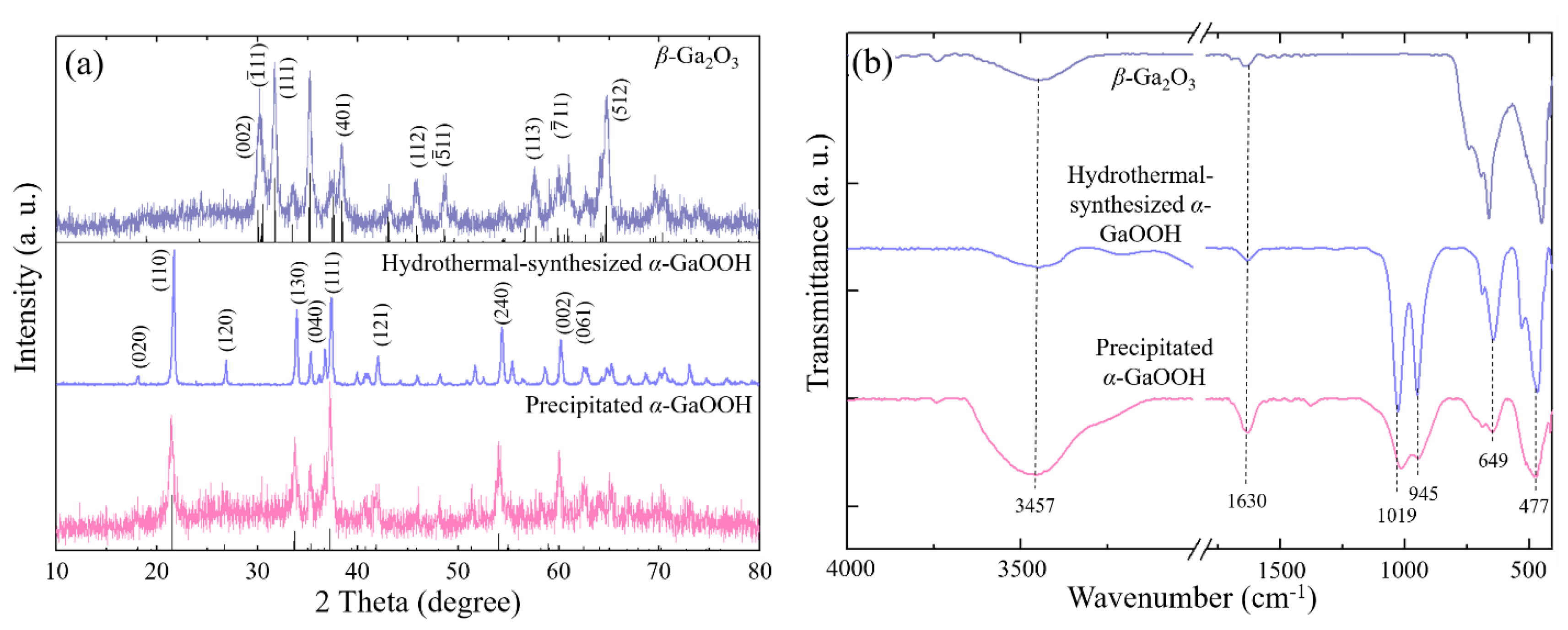
Figure 5.
(a) Histogram of the size distribution and (b) proposed growth mechanism of β-Ga2O3 nanorods depending at different aging times. Under the insufficient aging time (below 2 h in these experimental conditions), the uncompleted nanoparticles prevented the attachment of the spindle-like nanorods parallel to the plane, causing a prism-like nanord with nanoparticles. On the other hand, under the excessive aging time (above 3 h in these experimental conditons), the precipitated nanorods with smooth surfaces were continually and repeatedly dissolved and re-assembled in the supersaturated solution. The re-assembled nanorods at longer aging times presumably possessed more defects and mismatches, which also prevented the attachment of nanorods parallel to the plane and caused the crystal to split, leading to bundles of small nanorods of split structures.

Figure 6.
(a) output (IDS-VDS) and (b) transfer (IDS-VGS) characteristics of the Ga2O3 nanorod FETs. Inset image of (a): optical microscope image of β-Ga2O3 FET (source-drain distance: 10 μm). Inset image of (b): a schematic drawing of the bird’s eye view of the Ga2O3 FET. This limited current density the Ga2O3 nanorod FETs was comparable to the semi-insulating Ga2O3 bulk FETs without source and drain doping [51].

© 2018 by the authors. Licensee MDPI, Basel, Switzerland. This article is an open access article distributed under the terms and conditions of the Creative Commons Attribution (CC BY) license (http://creativecommons.org/licenses/by/4.0/).
Share and Cite
MDPI and ACS Style
Bae, H.J.; Yoo, T.H.; Yoon, Y.; Lee, I.G.; Kim, J.P.; Cho, B.J.; Hwang, W.S. High-Aspect Ratio β-Ga2O3 Nanorods via Hydrothermal Synthesis. Nanomaterials 2018, 8, 594. https://doi.org/10.3390/nano8080594
AMA Style
Bae HJ, Yoo TH, Yoon Y, Lee IG, Kim JP, Cho BJ, Hwang WS. High-Aspect Ratio β-Ga2O3 Nanorods via Hydrothermal Synthesis. Nanomaterials. 2018; 8(8):594. https://doi.org/10.3390/nano8080594
Chicago/Turabian StyleBae, Hyun Jeong, Tae Hee Yoo, Youngbin Yoon, In Gyu Lee, Jong Pil Kim, Byung Jin Cho, and Wan Sik Hwang. 2018. "High-Aspect Ratio β-Ga2O3 Nanorods via Hydrothermal Synthesis" Nanomaterials 8, no. 8: 594. https://doi.org/10.3390/nano8080594
Note that from the first issue of 2016, this journal uses article numbers instead of page numbers. See further details here.