Actively Tunable Terahertz Switches Based on Subwavelength Graphene Waveguide


School of Computer and Information, Hefei University of Technology, Hefei 230009, China
*
Authors to whom correspondence should be addressed.
Nanomaterials 2018, 8(9), 665; https://doi.org/10.3390/nano8090665
Submission received: 23 July 2018
/
Revised: 23 August 2018
/
Accepted: 24 August 2018
/
Published: 26 August 2018
(This article belongs to the Special Issue Graphene-Based Nanostructures and Optoelectronic Applications)
Abstract
:As a new field of optical communication technology, on-chip graphene devices are of great interest due to their active tunability and subwavelength scale. In this paper, we systematically investigate optical switches at frequency of 30 THz, including Y-branch (1 × 2), X-branch (2 × 2), single-input three-output (1 × 3), two-input three-output (2 × 3), and two-input four-output (2 × 4) switches. In these devices, a graphene monolayer is stacked on the top of a PMMA (poly methyl methacrylate methacrylic acid) dielectric layer. The optical response of graphene can be electrically manipulated; therefore, the state of each channel can be switched ON and OFF. Numerical simulations demonstrate that the transmission direction can be well manipulated in these devices. In addition, the proposed devices possess advantages of appropriate ON/OFF ratios, indicating the good performance of graphene in terahertz switching. These devices provide a new route toward terahertz optical switching.

1. Introduction
Actively tunable switches are among the key devices in optical communication systems and integrated circuits. A main category of switches in previous literature is based on waveguide structures, which is suitable for on-chip application. In this category, the switching mechanism relies on the modulation of optical properties of waveguide composite materials, such as electro- and thermo-optical materials [1,2,3]. One of the desired features of a switch is miniaturization, requiring deep subwavelength scales of both the waveguide structure and concentration of light. To this end, surface plasmon (SP) waveguides and metamaterials (metasurface) have been investigated and proposed to obtain optical switching devices [4,5,6,7,8]. However, metals also bring large intrinsic losses and metasurfaces are still bulky, restricting the practical application of SP switching.
Graphene has emerged as a fascinating alternative for metal due to its flexible tunability and high confinement of light with relatively low loss in the terahertz region [9,10,11]. By tuning the Fermi level, graphene may behave like a thin metal and strongly interact with incident light, thus motivating SPs along the surface of the graphene sheet. It can harness, squeeze, and manipulate electromagnetic waves via simply applying an external applied voltage, leading to the manipulation of graphene SPs at the graphene/dielectric interface [12,13]. These unique properties make graphene a suitable candidate for tunable and compact terahertz switching devices. Yarahmadi et al. proposed a subwavelength terahertz switch based on a Y-branch graphene/gold hybrid structure [14]. They further reported a graphene-based plasmonic waveguide, performing as a switch or an AND/OR logic gate at a frequency of 6 THz [15]. Wu et al. further designed all-optical logic devices based on graphene SPs to achieve six different basic logic gates by utilizing interference between the SPs wave in different channels [16]. Recently, Peng et al. proposed a general theoretical model to obtain the optimal solution for a linear-optical logic gate [17]. However, it is still urgent to develop terahertz switches with multiple-input multiple-output (MIMO) due to the requirement of the communication system to have a large capacity.
In this study, we systematically investigated different types of optical switches at a frequency of 30 THz, including Y-branch (1 × 2), X-branch (2 × 2), single-input three-output (1 × 3), two-input three-output (2 × 3), and two-input four-output (2 × 4) switches. These devices are based on graphene waveguides, consisting of a graphene monolayer, PMMA (poly methyl methacrylate methacrylic acid) interlayer, and silicon substrate. Numerical simulation results demonstrate that the effective optical response of the proposed waveguide structure can be tuned in the subwavelength scale via an external gate voltage, therefore achieving ON/OFF or “1/0” states. Based on this result, we further designed terahertz optical switches to realize several logic gates with the aid of an external gate voltage. We show that the transmission direction can be well manipulated, demonstrating the superior performance of graphene in terahertz switching.
2. Theory and Simulation Method
Figure 1a–e schematically show the Y-branch (1 × 2), X-branch (2 × 2), single-input three-output (1 × 3), two-input three-output (2 × 3), and two-input four-output (2 × 4) terahertz switches, respectively. The switches consist of graphene, PMMA, and silicon substrate, supporting graphene-based SPs. In this structure, the thickness of the silicon substrate and PMMA are set at 200 nm and 50 nm, respectively. Meanwhile, the graphene monolayer is treated as an ultrathin film layer with a thickness of Δ = 1 nm [18,19,20]. The permittivity of silicon and PMMA is 11.7 and 2.25, respectively. The relative permittivity of graphene is set as:
where is the permittivity in vacuum. In terahertz range, the surface conductivity of the monolayer graphene can be characterized by the Kubo formula [21] as a sum of two terms: . The first term corresponds to the intra-band electron-photon scattering is expressed as:
The second term corresponds to the inter-band transition contribution and is expressed as:
where e is the electron charge, is the Boltzmann’s constant, is the temperature, is the chemical potential, is the angular frequency, is the reduced Planck’s constant, and stands for the momentum relaxation time due to charge carrier scattering. The Fermi velocity is set at 106 m/s, and the carrier mobility of graphene is assumed as 4 m2/V·s at K [22,23]. In particular, the doping level of graphene shows a linear dependence on the external gate voltage as [24], where and are the relativity permittivity and thickness of PMMA, respectively, and is the external voltage.
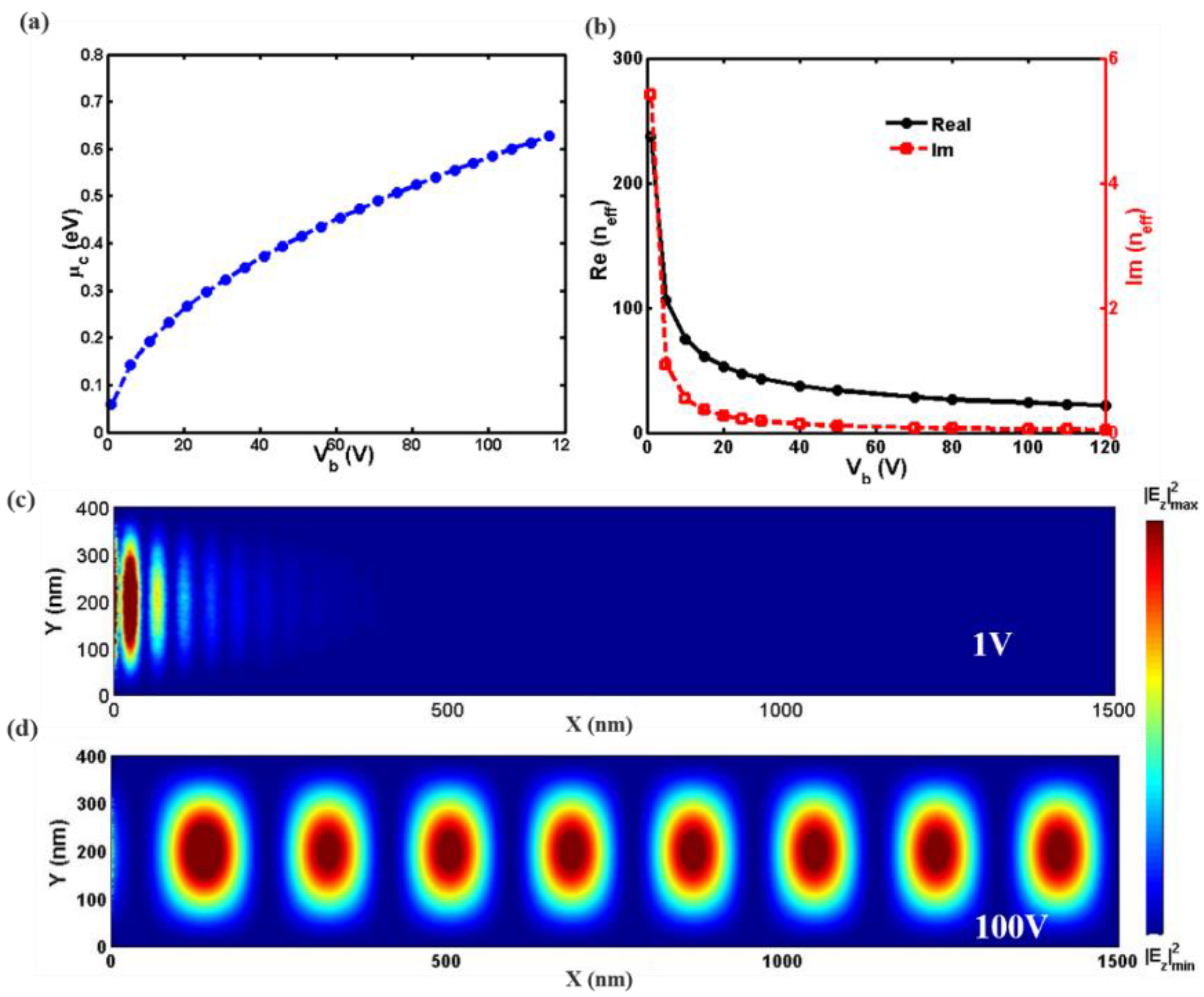
The above description indicates that we can control the optical conductivity of graphene by adjusting the external applied voltage or dielectric thickness. To demonstrate, we applied a voltage bias to the graphene/PMMA/Si, as schematically shown in Figure 1f. The dependence of the chemical potential on the bias voltage is plotted Figure 2a, presenting that an increased bias voltage (from 0 V to 120 V) results in a monotone increase of chemical potential.
As is well known, graphene sheets can behave optically similar to ultrathin metallic films; therefore, our approach could realize terahertz switches by utilizing graphene-based SPs. The influence of the Si substrate on the SP dispersion can be neglected in our proposed architectures due to the thick PMMA layer [25]. Therefore, the dispersion relation of graphene-based SPs can be derived as follows [26,27,28,29]:
where is the free-space wave vector of light, is the incident wavelength in vacuum, is the effective refractive index of the SP mode, denotes the relative permittivity of air, and is the relative permittivity of PMMA. Here, we set and . According to Equation (4), the surface conductivity of graphene determines the effective refractive index of the SP mode, which is extremely sensitive to and . Generally, the effective refractive index decreases with increasing due to the enlarged electric field. In the terahertz region, the surface conductivity of graphene can be simplified into the Drude-like form [12,19]. From the above equations, the real part of the effective refractive index can be approximated as:
Note that the above dispersion equation is obtained only considering the influence of external voltage [25]. Figure 2b shows that the effective refractive index of the graphene-based SPs can be electrically modified. The real part of the effective mode index decreases as the voltage bias increases, causing the reduction of SPs’ mode confinement. In addition, the imaginary part also decreases sharply as increases, which indicates that the propagation loss of SPs decreases [30,31,32,33,34]. Hence, it is expected that the longer propagation distance of the SPs occurs at a larger bias voltage.
To demonstrate the effectiveness of our designs, numerical simulations were performed using the finite element method. Noting that during the experimental fabrication, the chemical treatment and crystal growth direction may result in imperfections in the graphene, such as the formation of polycrystalline graphene from folding defects. This would improve the light absorption of graphene [35,36]. However, we only numerically investigate the ideal single layer graphene for simplicity. A plane wave at a frequency of 30 THz is normally incident from the −x direction. Graphene-based surface plasmons (GSPs) will be excited so that the electromagnetic energy is strongly concentrated near graphene and propagates along the graphene layer. Perfect matched layers have been used to absorb any reflected and transmitted field. As shown in Figure 2c, when the graphene is biased to , the SPs wave propagate a very short distance and no signal reaches the output port. This is labeled as the OFF or “0” state. As shown in Figure 2d, while the bias voltage increases to V, the SPs have a long wave propagation distance and can reach the output port. This is labeled as the ON or “1” state. Therefore, the propagation of the SPs wave can be switched ON or OFF (“1” or “0”) by modifying the bias voltage. To optimize our proposed optical switch, we investigated the dependence of the graphene waveguide and the working bandwidth was about 0.7 µm (not shown here). Accordingly, we chose the center wavelength to be 10 um. Subsequently, we demonstrated the potential of the proposed scheme for active switching in practical applications by designing several switches.
3. Results and Discussion
3.1. Y-Branch Switch
Based on the structure presented above, we designed a Y-branch (1 × 2) plasmonic switch, as shown in Figure 1a. The geometry parameters of the input block are W = 800 nm and L1 = 500 nm. The output block consists of two identical output ports with L1 = 1000 nm and L2 = 1500 nm. The bias voltage of the top graphene layer of the input block is kept at V. Figure 3a shows the electric field distributions when both output blocks are biased to . It is easy to see that both branch arms of the Y-block are OFF, corresponding to the “00” logic state. Figure 3b,c illustrates the electric field distributions of the “01” and “10” states, respectively, when one of the output blocks is biased to V and the other to V. When both arms are biasing with V, the switching is in the “11” state, as depicted in Figure 3d.
In order to investigate the performance of the Y-branch (1 × 2) switch, Table 1 summarizes the transmission coefficient of each output channel at different switch states, calculated by dividing the energy of the output side by that of the input side. For the high external voltage ( V) at the output branch, which is “1”, the transmission coefficient is about 10%. For the low external voltage ( V) at the output branch of transmission, the corresponding transmission coefficient is zero.
3.2. X-Branch Switch
Figure 1b schematically shows an X-branch (2 × 2) switch, in which the two input branches are “I” and “II”, and two output branches are “III” and “IV”. The geometry parameters were chosen as: W = 400 nm, h = 50 nm, L1 = 1000 nm, L2 = 500 nm, d1 = 200 nm. Due to the symmetry of the structure, we first took the example of branch “I” and “II” as the ON and OFF states, respectively. The states of “III” and “IV” can be well controlled due to the electrical tunability of graphene, as demonstrated in Figure 4a–c. When the external voltage of branch “III” is V, the input electromagnetic field from branch “I” can propagate along the output branch “III”. On the contrary, when the external voltage of branch “III” is set to V, it cannot propagate on this branch. In addition, we can see a similar response for branch “IV”. We also explored the condition when both branches “I” and “II” are in the ON state. Figure 4d,e further demonstrate that the output state can be switched to “00“ and “11“.
Table 2 summarizes the transmission coefficients of the output channels “III” and “IV” at different states. When a high voltage is applied at any output branch, the graphene-based SPs have a low propagation loss and high confinement. Therefore, the transmission coefficient of this output port will be at a high level, reaching the highest value of almost 40%. In contrast, when we set a low voltage at any output branch, the graphene-based SPs have an extremely high propagation loss. Thus, the transmission coefficient of the port is zero, corresponding to the OFF state, and there is no energy transmitted through this output branch.
3.3. Single-Input Three-Output Switch
Figure 1c shows the 1 × 3 switch, where the single input port is labeled as “I”, and three output branches are labeled as “II”, “III”, and “IV”. The geometry parameters were chosen as: W = 400 nm, W1 = 200 nm, h = 50 nm, d1 = 200 nm, L1 = 1000 nm, L2 = 500 nm. In Figure 5a–c, we obtained the state in which one of the output branches is ON and the other two are OFF. Specifically, we applied a high voltage of V at one arbitrary output branch and a low voltage of V at the other two output branches. In Figure 5a, the output branch “II” is ON and branches “III”, “IV” are OFF. Therefore, the input electromagnetic field can only pass through the output branch “II” and is prohibited in the other two output branches, which means that the total output state is displayed as “100”. Similarly, Figure 5b,c display the output states of “010” and “001”, respectively. In Figure 5d–f, we found that one of the output branches is OFF and the other two are ON. Specifically, we applied a low voltage of V at one arbitrary output branch and a high voltage of V at the other two output branches. For example, in Figure 5d, the branch “II” is OFF and the branches “III”, “IV” are ON. Therefore, the input electromagnetic field is prohibited in branch “II” and could pass through branches “III” and “IV”. This means that the total output state is displayed as “011”. Similarly, Figure 5e,f display the output states of “110” and “101”, respectively. Moreover, in Figure 5g,h, we showed the state in which all output branches are OFF and ON, meaning that the input electromagnetic is prohibited and can propagate through all output branches, respectively. The output states of Figure 5g,h are “000” and “111”, respectively.
Table 3 summarizes the transmission coefficients of output branches “II”, “III”, and “IV” for all output states. When we set a low voltage at the output branch, we observed that the transmission coefficient is zero, which is defined as the OFF state. When we set a high voltage at the output branch, we observed that the transmission coefficient is high, which is defined as the ON state. Note that, although there is a transmission coefficient of about 2%, it still much higher than the OFF state (zero). Thus, we can still use this structure as an optical switch.
3.4. Two-Input Three-Output Switch
We know that multiple-input multiple-output technology is one of the key features to extend the capacity of a communication system. Therefore, we further investigated a two-input three-output (2 × 3) switch, as schematically shown in Figure 1d. The geometry parameters were chosen as: W0 = 600 nm, W1 = 400 nm, W2 = 200 nm, h = 50 nm, d1 = 200 nm, L1 = 1000 nm, L2 = 500 nm. The stimulated SP wave can be coupled into the output branch. The biasing conditions determine whether the output branches are ON or OFF. Because of the structural symmetry, we took the example of input branches “I” and “II” as ON and OFF, respectively, corresponding to the input state of “10”. Figure 6a–f show the electric field distributions when we control the external voltage to determine whether the electromagnetic field can pass through the output branches “III”, “IV”, and “V”, obtaining corresponding output states. In Figure 6a–c, the output branches are in the logical states of “100”, “010”, and “001”, respectively. We further obtained the output states “110”, “101”, and “011” in Figure 6d–f, respectively. In Figure 6g,h, we demonstrate that the three output branches can be OFF and ON at the same time, corresponding to the output states of “000” and “111”, respectively.
Table 4 summarizes the transmission coefficients of the output channels “III”, “IV”, and “V” at different logical states. When we set a low voltage ( V) at each output branch, corresponding to the OFF state, the transmission coefficient is zero. When we set a high voltage ( V) at each output branch, corresponding to the ON state, the transmission coefficient can be much higher. Although there is a lowest transmission coefficient of about 2%, it still relatively higher than that of the OFF state (zero). Therefore, we can still consider this simple transmission line as a 2 × 3 optical switch.
3.5. Two-Input Four–Output Switch
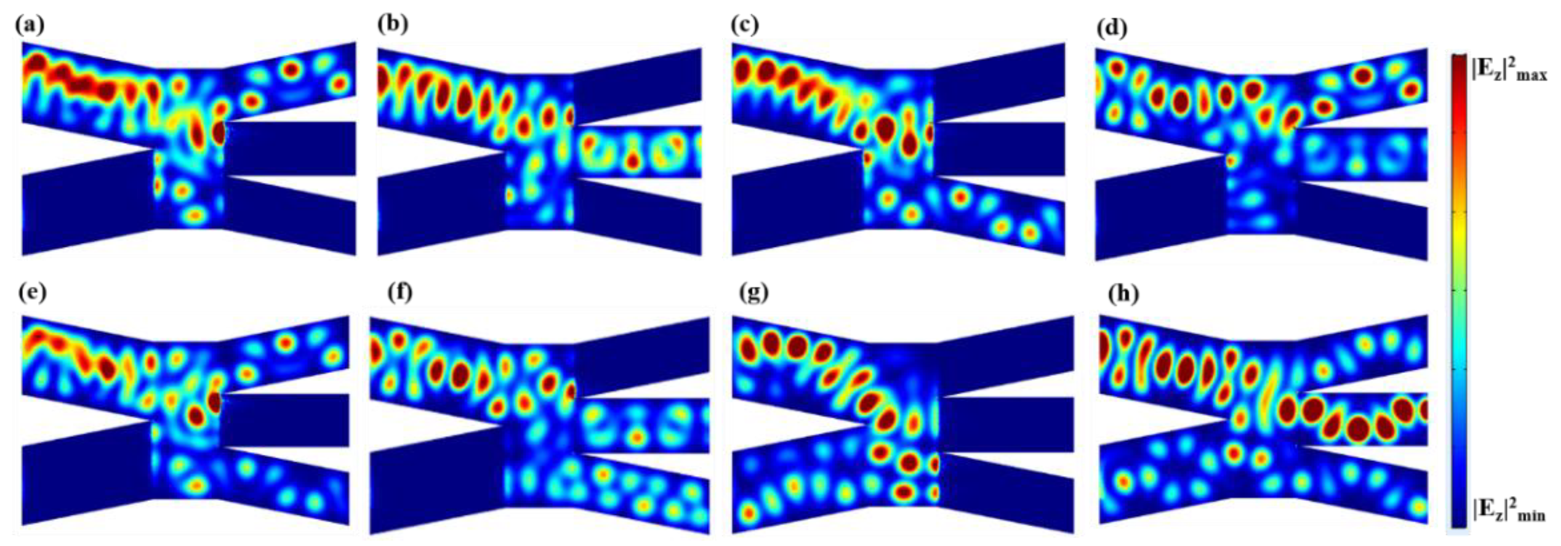
We applied the proposed structure to a two-input four-output (2 × 4) switch, as shown in Figure 1e. The geometry parameters were chosen as: W0 = 800 nm, W1 = 200n m, W2 = 400 nm, W3 = 100 nm, h = 50 nm, d1 = 200 nm, L1 = 1000 nm, L2 = 500 nm. Figure 7 shows the electric field distribution of the switch at different input and output states. Firstly, we considered the case in which the input branches “I” and “II” are ON and OFF, respectively. Figure 7a–f show the electric field distributions when we control the external voltage to determine whether the electromagnetic field can pass through the output branches “III”, “IV”, “V”, and “VI”. For the case in which only one output branch is ON, we took the example of an electric field that is controlled to propagate in either branch “III” or “VI”. Therefore, the corresponding output states of “1000” and “0001” are achieved, as shown in Figure 7a,b, respectively. For the case in which two output branches are ON, we took the example of an electric field that is controlled to propagate in either branches “III”, “IV” or “IV”, “V”. This corresponds to the output states of “1100” and “0110”, as shown in Figure 7c,d, respectively. We further investigated the case in which three output branches are ON. As examples, we showed that the electromagnetic field can pass through either branches “III”, “IV”, “V” or “IV”, “V”, “VI”, corresponding to the output states of “1110” or “0111”, as shown in Figure 7e,f, respectively. In Figure 7g,h, we further demonstrated that the four output branches can be OFF and ON at the same time, corresponding to output states of “0000” and “1111”, respectively.
Table 5 summarizes the transmission coefficients of output channels “III”–“VI”. When an output branch is OFF, no input energy can propagate in it and the transmission coefficient is zero. When an output branch is ON, the input energy can pass through it due to the low loss of graphene SPs. Even though the transmission coefficient is only about 2%, we can still consider the structure to be an optical switch. In future study, we will continue to explore the transmittance efficiency issue to further optimize the present work.
4. Conclusions
In summary, we have theoretically and numerically investigated multiple-input multiple-output switches. The applied gate voltage can be employed to tune the conductivity of graphene to control whether it can be propagated at the graphene surface. Moreover, each branch can realize an ON/OFF state by adjusting the external voltage. Thus, we designed a Y-branch plasmonic waveguide to realize a single-input two-output switch by biasing an appropriate voltage at the graphene layer and Si substrate. We also designed X-branch (2 × 2), single-input three-output (1 × 3), two-input three-output (2 × 3), and two-input four-output (2 × 4) switches to realize multiple-input multiple-output transmission. All of the proposed structures together demonstrate good switching performances with high controllability and subwavelength confinement of electromagnetic waves. These structures can be widely used in the manipulation of information propagation and optical switches, and have far-reaching significance.
Author Contributions
Investigation, Z.G. and X.N.; Resources, F.S, H.Z, Q.Z, and J.G.; Writing—Review and Editing, K.G.; Supervision, K.G.
Funding
This research was funded by the National Natural Science Foundation of China (61775050 and 11505043), Science and Technology Planning Project of Guangdong Province, China (2016B010108002), Natural Science Foundation of Anhui Province, China (Grant No. 1808085MF188 and 1808085QA21), and Fundamental Research Funds for the Central Universities (JD2017JGPY0005, JZ2018HGBZ0309, and JZ2018HGTB0240).
Conflicts of Interest
The authors declare no conflict of interest.
References
- Zhou, J.; Wong, W.; Pun, E.; Shen, Y. Fabrication of low loss optical waveguides with a novel thermo-optical polymer material. Opt. Appl. 2006, 36, 429–435. [Google Scholar]
- Vicente, C.; Lima, P.; Bermudez, V.; Carlos, L.; André, P.; Ferreira, R. Fabrication of low-cost thermo-optic variable wave plate based on waveguides patterned on di-ureasil hybrids. Opt. Express 2014, 22, 27159–27168. [Google Scholar] [CrossRef] [PubMed]
- Stolte, R.; Ulrich, R. Electro-optic and thermo-optic measurements of birefringence of LiNbO3 waveguides. Opt. Lett. 1995, 20, 142–144. [Google Scholar] [CrossRef] [PubMed]
- Guo, Z.; Xu, H.; Guo, K.; Shen, F.; Zhou, H.; Zhou, Q.; Gao, J.; Yin, Z. High-efficiency visible transmitting polarizations devices based on the GaN metasurface. Nanomaterials 2018, 8, 333. [Google Scholar] [CrossRef] [PubMed]
- Yin, Z.; Chen, F.; Zhu, L.; Guo, K.; Shen, F.; Zhou, Q.; Guo, Z. High-efficiency dielectric metasurfaces for simultaneously engineering polarization and wavefront. J. Mater. Chem. C 2018, 6, 6354–6359. [Google Scholar] [CrossRef]
- Ozbay, E. Plasmonics: Merging photonics and electronics at nanoscale dimensions. Science 2006, 311, 189–193. [Google Scholar] [CrossRef] [PubMed]
- Ge, C.; Guo, Z.; Sun, Y.; Shen, F.; Tao, Y.; Zhang, J.; Li, R.; Luo, L. Spatial and spectral selective characteristics of the plasmonic sensing using metallic nanoslit arrays. Opt. Commun. 2016, 359, 393–398. [Google Scholar] [CrossRef]
- Zheng, Y.B.; Yang, Y.W.; Jensen, L.; Fang, L.; Juluri, B.K.; Flood, A.H.; Weiss, P.S.; Stoddart, J.F.; Huang, T.J. Active molecular plasmonics: Controlling plasmon resonances with molecular switches. Nano Lett. 2009, 9, 819–825. [Google Scholar] [CrossRef] [PubMed]
- Koppens, F.H.; Chang, D.E.; Garcia de Abajo, F.J. Graphene plasmonics: A platform for strong light–matter interactions. Nano Lett. 2011, 11, 3370–3377. [Google Scholar] [CrossRef] [PubMed]
- Gusynin, V.P.; Sharapov, S.G.; Carbotte, J.P. Magneto-optical conductivity in graphene. J. Phys. Condens. Matter 2006, 19, 026222. [Google Scholar] [CrossRef] [Green Version]
- Chen, J.; Jang, C.; Xiao, S.; Ishigami, M.; Fuhrer, M.S. Intrinsic and extrinsic performance limits of graphene devices on SiO2. Nat. Nanotechnol. 2008, 3, 206–209. [Google Scholar] [CrossRef] [PubMed]
- Chen, P.; Alu, A. Atomically thin surface cloak using graphene monolayers. ACS Nano 2011, 5, 5855–5863. [Google Scholar] [CrossRef] [PubMed]
- Ju, H.; Bing, W.; Jiang, Y.; Gao, Z. Beam-scanning planar lens based on graphene. Appl. Phys. Lett. 2012, 100, 051903. [Google Scholar] [CrossRef]
- Yarahmadi, M.; Moravvej-Farshi, M.; Yousefi, L. Compact low power graphene-based Y-branch THz switch. In Proceedings of the Third Conference on IEEE Millimeter-Wave and Terahertz Technologies, Tehran, Iran, 30 December–1 January 2015. [Google Scholar]
- Yarahmadi, M.; Moravvej-Farshi, M.K.; Yousefi, L. Subwavelength graphene-based plasmonic THz switches and logic gates. IEEE Trans. Terahertz Sci. Technol. 2015, 5, 725–731. [Google Scholar] [CrossRef]
- Wu, X.; Tian, J.; Yang, R. A type of all-optical logic gate based on graphene surface plasmon polaritons. Opt. Commun. 2017, 403, 185–192. [Google Scholar] [CrossRef]
- Peng, C.; Li, J.; Liao, H.; Li, Z.; Sun, C.; Chen, J.; Gong, Q. Universal linear-optical logic gate with maximal intensity contrast ratios. ACS Photonics 2018, 5, 1137–1143. [Google Scholar] [CrossRef]
- Shi, B.; Cai, W.; Zhang, X.; Xiang, Y.; Zhan, Y.; Geng, J.; Ren, M.; Xu, J. Tunable band-stop filters for graphene plasmons based on periodically modulated graphene. Sci. Rep. 2016, 6, 26796. [Google Scholar] [CrossRef] [PubMed]
- Hao, R.; Peng, X.; Li, E.; Xu, Y.; Jin, J.; Zhang, X.; Chen, H. Improved slow light capacity in graphene-based waveguide. Sci. Rep. 2015, 5, 15335. [Google Scholar] [CrossRef] [PubMed]
- Zhang, F.M.; He, Y.; Chen, X. Guided modes in graphene waveguides. Appl. Phys. Lett. 2009, 94, 212105. [Google Scholar] [CrossRef]
- Christensen, J.; Manjavacas, A.; Thongrattanasiri, S.; Koppens, F.H.; García de Abajo, F.J. Graphene plasmon waveguiding and hybridization in individual and paired nanoribbons. ACS Nano 2011, 6, 431–440. [Google Scholar] [CrossRef] [PubMed]
- Bolotin, K.; Sikes, K.; Jiang, Z.; Klima, M.; Fudenberg, G.; Hone, J.; Kim, P.; Stormer, H. Ultrahigh electron mobility in suspended graphene. Solid State Commun. 2008, 146, 351–355. [Google Scholar] [CrossRef] [Green Version]
- Qiu, W.; Liu, X.; Zhao, J.; Huang, Y.; Chen, H.; Li, B.; Wang, J.; Pan, J.Q. Ultrabroad band rainbow capture and releasing in graded chemical potential distributed graphene monolayer. Plasmonics 2015, 10, 1023–1028. [Google Scholar] [CrossRef]
- Novoselov, K.S.; Geim, A.K.; Morozov, S.V.; Jiang, D.A.; Zhang, Y.; Dubonos, S.V.; Grigorieva, I.V.; Firsov, A.A. Electric field effect in atomically thin carbon films. Science 2004, 306, 666–669. [Google Scholar] [CrossRef] [PubMed]
- Lu, H.; Zeng, C.; Zhang, Q.; Liu, X.; Hossain, M.M.; Reineck, P.; Gu, M. Graphene-based active slow surface plasmon polaritons. Sci. Rep. 2015, 5, 8443. [Google Scholar] [CrossRef] [PubMed] [Green Version]
- Jablan, M.; Buljan, H.; Soljačić, M. Plasmonics in graphene at infrared frequencies. Phys. Rev. B 2009, 80, 245435. [Google Scholar] [CrossRef]
- De Oliveira, R.E.; De Matos, C.J. Graphene based waveguide polarizers: In-depth physical analysis and relevant parameters. Sci. Rep. 2015, 5, 16949. [Google Scholar] [CrossRef] [PubMed]
- Luo, L.; Wang, K.; Guo, K.; Shen, F.; Zhang, X.; Yin, Z.; Guo, Z. Tunable manipulation of terahertz wavefront based on graphene metasurfaces. J. Opt. 2017, 19, 115104. [Google Scholar] [CrossRef] [Green Version]
- Wang, J.; Song, C.; Hang, J.; Hu, Z.D.; Zhang, F. Tunable Fano resonance based on grating-coupled and graphene-based Otto configuration. Opt. Express 2017, 25, 23880–23892. [Google Scholar] [CrossRef] [PubMed]
- Wang, W.; Meng, Z.; Liang, R.; Chen, S.; Ding, L.; Wang, F.; Liu, H.; Wei, Z. A dynamically tunable plasmonic multi-functional device based on graphene nano-sheet pair arrays. Opt. Commun. 2018, 415, 130–134. [Google Scholar] [CrossRef]
- Luo, L.; Wang, K.; Ge, C.; Guo, K.; Shen, F.; Yin, Z.; Guo, Z. Actively controllable terahertz switches with graphene-based nongroove gratings. Photonics Res. 2017, 5, 604–611. [Google Scholar] [CrossRef]
- Wang, J.; Wang, X.; Hu, Z.D.; Zheng, G.; Zhang, F. Peak modulation in multi-cavity-coupled graphene-based waveguide system. Nanoscale Res. Lett. 2017, 12. [Google Scholar] [CrossRef]
- Gómez-Díaz, J.S.; Perruisseau-Carrier, J. Graphene-based plasmonic switches at near infrared frequencies. Opt. Express 2013, 21, 15490–15504. [Google Scholar] [CrossRef] [PubMed]
- Yang, J.; Xin, H.; Han, Y.; Chen, D.; Zhang, J.; Huang, J.; Zhang, Z. Ultra-compact beam splitter and filter based on a graphene plasmon waveguide. Appl. Opt. 2017, 56, 9814–9821. [Google Scholar] [CrossRef] [PubMed]
- Lim, G.; Kihm, K.D.; Kim, H.G.; Lee, W.; Lee, W.; Pyun, K.R.; Cheon, S.; Lee, P.; Min, J.Y.; Ko, S.H. Enhanced thermoelectric conversion efficiency of CVD graphene with reduced grain sizes. Nanomaterials 2018, 8, 557. [Google Scholar] [CrossRef] [PubMed]
- Kim, K.; Lee, H.; Johnson, R.W.; Tanskanen, J.T.; Liu, N.; Kim, M.G.; Pang, C.; Ahn, C.; Bent, S.F.; Bao, Z. Selective metal deposition at graphene line defects by atomic layer deposition. Nat. Commun. 2014, 5, 4781. [Google Scholar] [CrossRef] [PubMed] [Green Version]
Figure 1.
(a) Schematic of the Y-branch switch structure. W = 800 nm, h = 50 nm, L1 = 500 nm, L2 = 1000 nm, L3 = 1500 nm, W1 = W2 = 400 nm; (b) Schematic of the X-branch switch structure. W = 400 nm, h = 50 nm, L1 = 1000 nm, L2 = 500 nm, d1 = 200 nm; (c) Schematic of the single-input three-output structure. W = 400 nm, W1 = 200 nm, h = 50 nm, d1 = 200 nm, L1 = 1000 nm, L2 = 500 nm; (d) Schematic of the two-input three-output structure. W0 = 600 nm, W1 = 400 nm, W2 = 200 nm, h = 50 nm, d1 = 200 nm, L1 = 1000 nm, L2 = 500 nm; (e) Schematic of the two-input four-output structure. W0 = 800 nm, W1 = 200 nm, W2 = 400 nm, W3 = 100 nm, h = 50 nm, d1 = 200 nm, L1 = 1000 nm, L2 = 500 nm; (f) Schematic illustration of applying the bias voltage.

Figure 2.
(a) Dependence of chemical potential on the bias voltage with h = 50 nm; (b) The real and imaginary parts of the effective index of graphene-based surface plasmons (SPs) as functions of the gate voltage . Distributions of |Ez|2 in the x-y plane of the waveguide (h = 50 nm, f = 30 THz), in the (c) OFF and (d) ON states.

Figure 3.
Distributions of |Ez|2 in the x-y plane of the Y-branch switch, in the output logical state of (a) “00”; (b) “01”; (c) “10”; and (d) “11”.
Figure 3.
Distributions of |Ez|2 in the x-y plane of the Y-branch switch, in the output logical state of (a) “00”; (b) “01”; (c) “10”; and (d) “11”.

Figure 4.
Distributions of |Ez|2 in the x-y plane of the X-branch switch. When the input branches “I” and “II” are ON and OFF, respectively, corresponding to input state of “10”, the output branches are in the logical states of (a) “01”; (b) “10”; and (c) “11”. When the input branches “I” and “II” are both ON, corresponding to input state of “11”, the output branches are in the logical states of (d) “00” and (e) “11”.

Figure 5.
Distributions of |Ez|2 in the x-y plane of the single-input three-output switch, in the output logical states of (a) “100”; (b) “010”; (c) “010”; (d) “011”; (e) “110”; (f) “101”; (g) “000” and (f) “111”.
Figure 5.
Distributions of |Ez|2 in the x-y plane of the single-input three-output switch, in the output logical states of (a) “100”; (b) “010”; (c) “010”; (d) “011”; (e) “110”; (f) “101”; (g) “000” and (f) “111”.

Figure 6.
Distributions of |Ez|2 in the x-y plane of the two-input three-output switch. When the input branches “I” and “II” are ON and OFF, respectively, corresponding to input states of “10”, the output branches are in the logical states of (a) “100”; (b) “010”; (c) “001”; (d) “110”; (e) “101”; and (f) “011”. When the input branches “I” and “II” are both ON, corresponding to the input state of “11”, the output branches are in the logical states of (g) “000” and (h) “111”.

Figure 7.
Distributions of |Ez|2 in x-y plane of the two-input four-output switch. When the input branches “I” and “II” are ON and OFF, respectively, corresponding to the input state of “10”, the output branches are in the logical states of (a) “1000”; (b) “0001”; (c) “1100”; (d) “0110”; (e) “0111” and (f) “0111”. When the input branches “I” and “II” are both ON, corresponding to input state of “11”, the output branches are in the logical states of (g) “0000” and (h) “1111”.


Table 1.
Transmission coefficients of the Y-branch switch at different logical states.
| Output Signal | Transmission Coefficient (%) | ||
|---|---|---|---|
| Output II | Output III | Output II | Output III |
| 0 | 0 | 0 | 0 |
| 1 | 0 | 14.418 | 0 |
| 0 | 1 | 0 | 13.872 |
| 1 | 1 | 9.589 | 13.042 |
Table 2.
Transmission coefficients of the X-branch switch at different logical states.
| Input Signal | Output Signal | Transmission Coefficient (%) | |||
|---|---|---|---|---|---|
| Input I | Input II | Output III | Output IV | Output III | Output IV |
| 1 | 0 | 0 | 1 | 0 | 9.775 |
| 1 | 0 | 1 | 0 | 27.221 | 0 |
| 1 | 0 | 1 | 1 | 36.785 | 13.004 |
| 1 | 1 | 0 | 0 | 0 | 0 |
| 1 | 1 | 1 | 1 | 27.016 | 49.695 |
Table 3.
Transmission coefficients of the single-input three-output switch at different logical states.
Table 3.
Transmission coefficients of the single-input three-output switch at different logical states.
| Input Signal | Output Signal | Transmission Coefficient (%) | ||||
|---|---|---|---|---|---|---|
| Input I | Output II | Output III | Output IV | Output II | Output III | Output IV |
| 1 | 1 | 0 | 0 | 5.557 | 0 | 0 |
| 1 | 0 | 1 | 0 | 0 | 58.527 | 0 |
| 1 | 0 | 0 | 1 | 0 | 0 | 3.848 |
| 1 | 0 | 1 | 1 | 0 | 70.106 | 2.011 |
| 1 | 1 | 1 | 0 | 2.215 | 63.966 | 0 |
| 1 | 1 | 0 | 1 | 4.011 | 0 | 3.145 |
| 1 | 0 | 0 | 0 | 0 | 0 | 0 |
| 1 | 1 | 1 | 1 | 1.743 | 54.373 | 3.835 |
Table 4.
Transmission coefficients of the two-input three-output switch at different logical states.
Table 4.
Transmission coefficients of the two-input three-output switch at different logical states.
| Input Signal | Output Signal | Transmission Coefficient (%) | |||||
|---|---|---|---|---|---|---|---|
| Input I | Input II | Output III | Output IV | Output V | Output III | Output IV | Output V |
| 1 | 0 | 1 | 0 | 0 | 6.913 | 0 | 0 |
| 1 | 0 | 0 | 1 | 0 | 0 | 20.86 | 0 |
| 1 | 0 | 0 | 0 | 1 | 0 | 0 | 1.183 |
| 1 | 0 | 1 | 1 | 0 | 1.391 | 13.566 | 0 |
| 1 | 0 | 1 | 0 | 1 | 1.29 | 0 | 4.502 |
| 1 | 0 | 0 | 1 | 1 | 0 | 19.722 | 9.884 |
| 1 | 1 | 0 | 0 | 0 | 0 | 0 | 0 |
| 1 | 1 | 1 | 1 | 1 | 6.281 | 30.536 | 7.833 |
Table 5.
Transmission coefficients of the two-input four-output switch at different logical states.
| Control Signal | Output Signal | Transmission Coefficient (%) | |||||||
|---|---|---|---|---|---|---|---|---|---|
| Input I | Input II | Output III | Output IV | Output V | Output VI | Output III | Output IV | Output V | Output VI |
| 1 | 0 | 1 | 0 | 0 | 0 | 0.157 | 0 | 0 | 0 |
| 1 | 0 | 0 | 0 | 0 | 1 | 0 | 0 | 0 | 0.172 |
| 1 | 0 | 0 | 1 | 1 | 0 | 0 | 0.105 | 1.394 | 0 |
| 1 | 0 | 1 | 1 | 0 | 0 | 1.688 | 0.161 | 0 | 0 |
| 1 | 0 | 1 | 1 | 1 | 0 | 0.114 | 0.279 | 0.01 | 0 |
| 1 | 0 | 0 | 1 | 1 | 1 | 0 | 0.317 | 0.012 | 0.026 |
| 1 | 1 | 0 | 0 | 0 | 0 | 0 | 0 | 0 | 0 |
| 1 | 1 | 1 | 1 | 1 | 1 | 0.0805 | 0.376 | 0.486 | 0.0886 |
© 2018 by the authors. Licensee MDPI, Basel, Switzerland. This article is an open access article distributed under the terms and conditions of the Creative Commons Attribution (CC BY) license (http://creativecommons.org/licenses/by/4.0/).
Share and Cite
MDPI and ACS Style
Guo, Z.; Nie, X.; Shen, F.; Zhou, H.; Zhou, Q.; Gao, J.; Guo, K. Actively Tunable Terahertz Switches Based on Subwavelength Graphene Waveguide. Nanomaterials 2018, 8, 665. https://doi.org/10.3390/nano8090665
AMA Style
Guo Z, Nie X, Shen F, Zhou H, Zhou Q, Gao J, Guo K. Actively Tunable Terahertz Switches Based on Subwavelength Graphene Waveguide. Nanomaterials. 2018; 8(9):665. https://doi.org/10.3390/nano8090665
Chicago/Turabian StyleGuo, Zhongyi, Xiaoru Nie, Fei Shen, Hongping Zhou, Qingfeng Zhou, Jun Gao, and Kai Guo. 2018. "Actively Tunable Terahertz Switches Based on Subwavelength Graphene Waveguide" Nanomaterials 8, no. 9: 665. https://doi.org/10.3390/nano8090665
Note that from the first issue of 2016, this journal uses article numbers instead of page numbers. See further details here.