Article

Protective Properties of a Microstructure Composed of Barrier Nanostructured Organics and SiOx Layers Deposited on a Polymer Matrix

1
Institute of Materials Science, Faculty of Chemistry, Brno University of Technology, Purkynova 464/118, 612 00 Brno, Czech Republic
2
Nuclear, Biological and Chemical Defence Institute of the University of Defence, Sidliste Vita Nejedleho, 68201 Vyškov, Czech Republic
3
DEZA, Hochmanova 1, 628 01 Brno, Czech Republic
4
Institute of Analytical Chemistry, Faculty of Chemical and Food Technology, Slovak University of Technology in Bratislava, Radlinskeho 9, 812 37 Bratislava, Slovakia
5
Department of Military Chemical Engineering, Military Academy, GeneralaPavlaJurisicaSturma 33, 11000 Belgrade, Serbia
6
P A R D A M, Ltd., Zizkova 2494, 413 01 Roudnicenad Labem, Czech Republic
*
Author to whom correspondence should be addressed.
Nanomaterials 2018, 8(9), 679; https://doi.org/10.3390/nano8090679
Submission received: 25 June 2018 / Revised: 28 August 2018 / Accepted: 29 August 2018 / Published: 31 August 2018
(This article belongs to the Special Issue Design and Development of Nanostructured Thin Films)

Abstract

:
The SiOx barrier nanocoatings have been prepared on selected polymer matrices to increase their resistance against permeation of toxic substances. The aim has been to find out whether the method of vacuum plasma deposition of SiOx barrier nanocoatings on a polyethylene terephthalate (PET) foil used by Aluminium Company of Canada (ALCAN) company (ALCAN Packaging Kreuzlingen AG (SA/Ltd., Kreuzlingen, Switzerland) within the production of CERAMIS® packaging materials with barrier properties can also be used to increase the resistance of foils from other polymers against the permeation of organic solvents and other toxic liquids. The scanning electron microscopy (SEM) microstructure of SiOx nanocoatings prepared by thermal deposition from SiO in vacuum by the Plasma Assisted Physical Vapour Deposition (PA-PVD) method or vacuum deposition of hexamethyldisiloxane (HMDSO) by the Plasma-enhanced chemical vapour deposition (PECVD) method have been studied. The microstructure and behavior of samples when exposed to a liquid test substance in relation to the barrier properties is described.

1. Introduction

Multilayer structures generally increase the protective properties of barrier materials [1,2,3,4]. The effect of a combination of the location of the barrier layers on the Protection Factor (BF) is shown in Figure 1.
Within the production of packaging materials for sensitive commodities and in chemical protection, this principle has been used for many years [5,6]. Multilayer barrier materials usually have better performance properties than the individual components from which they are made [7,8]. They are mostly cheaper and better processed [9,10,11]. This principle is also used by Aluminium Company of Canada (ALCAN) company in the production of SiOx-based CERAMIS® [12] packaging materials, which form a barrier layer between polymer foils (usually polyethylene terephthalate (PET) and polypropylene (PP)) during their lamination [13,14,15,16]. The principle of this technology of reactivating steaming the SiOx barrier layer from the SiO substrate in vacuum is illustrated in Figure S1.
In the Aluminium Company of Canada (ALCAN) brochure, this packaging material states that it creates an excellent barrier against gaseous and liquid harmful substances, independent of temperature and humidity. It is transparent for microwaves, suitable for heat sterilization and pasteurization, printable by common printing processes and it allows detection of metals. Due to the patented SiOx barrier coating technology used by ALCAN was not available, one of the obtained samples was evaluated for protective properties against sulphur mustard (HD) and 1,6-dichlorohexane (DCH). For a CERAMIS® CO 20 sample weighing 18.2 g/m2 (PET 12 μm, SiOx 60 nm, PP 20 μm), the protective properties against the permeation of HD and DCH have been found to be greater than 70 h.
Although this material exhibits high resistance to the permeation of selected toxic compounds, it has one major disadvantage from the point of view of its possible utility in anti-gas protection. Its considerable stiffness and imprecision does not allow it to be used for the construction of protective clothing. It was therefore the effort to apply the SiOx barrier layer to more suitable polymeric matrices.
Vacuum plasma deposition technology of barrier layers within normal temperatures is particularly suitable for the preparation of advanced surfaces with specific properties on flexible polymer and textile substrates [17,18,19,20]. A synoptical example of this advanced technology is the advanced novoFlex®600 equipment for coating polymeric materials in the footage developed by the Fraunhofer Institute for Organic Electronics, Electron Beam and Plasma Technology FEP (Dresden, Germany).
Another way to prepare SiOx barrier nanolayers on polymeric or textile materials is a method of plasma deposition from a mixture of siloxane substrates and oxygen. As the suitable substrates hexamethyldisiloxane (HMDSO) and tetraethylorthosilicate (TEOS), which most closely approximate to the structure of SiOx are considered [21].
The barrier layers could be prepared as flexible based on polymeric materials. One of the materials is Parylene. It is a commercial name for the group of poly-p-xylylene polymers. Dimmer ofpoly-p-xylylene is thermally evaporated (sublimated) from a powder within a low pressure of tens of Pascals. Steams of this dimmer joint a pyrolitic chamber. Within the temperature of approximately 680 °C comes to the split of the dimmer on monomer units. These molecules are reactive and devaporate on the surface of coated materials (in the same way as on walls of the reactive chamber). They polymerize in radical mechanism and form a linear polymeric polymer that is deposited as a very thin barrier layer. This layer is very homogenous and inert. The deposition of parylene was first observed by Szwarc in 1947, and Gorham later described a more efficient, general synthetic way to prepare poly-p-xylylene through the vacuum vapour-phase pyrolysis of paracyclophane at has been used till nowadays [22,23]. This polymerisation is self-initiated and non-terminated, requires no solvent or catalyst, produces no by-products except for the unreacted precursor. The polymer thin film is deposited spontaneously at the room temperature thus no thermal stress is induced in a coated object. Recently, parylene is one of the most well-known chemical vapour deposited (CVD) polymers and number of its applications has grown dramatically over the years.
The excellent resistance of polymeric packaging materials with the SiOx barrier layer against the permeation of oxygen and humidity has conducted to the conception that the plasma deposition of SiOxnanolayer and/or parylene film on the suitable polymeric matrix could be used for preparation of even constructive materials for protective garments resistant against toxic liquids and gases. This phenomenon has become a subject of our research. The aim of the study was to test these structures on the various polymers be used to increase the resistance against the permeation of organic solvents and other toxic liquids. The swelling of the polymeric substrate and material of nanostructured films is the main problem of barrier films functionality because of some destructions.

2. Materials and Methods

2.1. Source Materials, Substrates and Polymeric Matrices

SiO powder provided by Merck KGaA (Darmstadt, Germany) was used as source material for Plasma Assisted Physical Vapour Deposition (PA-PVD) process, hexamethyldi-siloxane (HMDSO) CAS 107-46-0 (Sigma-Aldrich, Prague, Czech Republic) was utilized as source materials for PE-CVD method. For PVD process of organics film the 1,3,5-triazine-2,4,6-triamine (melamine), CAS 108-78-1 (Sigma-Aldrich, Prague, Czech Republic) was used. Dimer of chlorinated p-xylylene (parylene C) (KunShanZhangShengNaNo Tech Company, Kunshan, China), CAS 28804-46-8 was utilized as source material for CVD method. Bis(2-chloroethyl) sulphide (sulphur mustard, HD) CAS 505-60-2 (Military Technical Institute of Protection, Brno, Czech Republic) and 1,6-Dichlorohexane CAS 218-491-7 (Sigma-Aldrich, Prague, Czech Republic) were used as test chemicals for verification of the quality of new developed barrier materials with nanolayers. Polyvinylidenchlorid (PVDC), CAS 9002-85-1 foil of 20 µm was used for lamination of PEVA foil. Thin films were prepared on polymeric foils from polyethylenevinyl acetate (PEVA), CAS 24937-78-8, foil of 200 µm thickness, polypropylene (PP) foil of 30 um thickness and polyethylentereftalate (PET) foil of 8 µm thickness. Si wafer WFP 6005 provided by ON Semiconductor (ON Semiconductor Czech Republic, Rožnov pod Radhoštěm, Czech Republic) was used as substrate for thin film characterization by energy-dispersive X-ray spectroscopy—EDX (ON Semiconductor Czech Republic, Ltd., Rožnov pod Radhoštěm, Czech Republic). EDX is a part of Scanning Electron Microscope ZEISS EVO LS 10 (Oberkochen, Germany). This spectroscopy provides elemental information about the composition of the structure of the surface of a sample. Performed in conjunction with SEM. Elements with atomic numbers down to carbon can be viewed with Energy Dispersive Spectroscopy (EDS).

2.2. Apparatuses for the Samples Preparation

The equipment for thermal lamination of plastic films without the use of binders was used as method for special multilayer structure fabrication. The original vacuum apparatus (Faculty of Chemistry, Brno University of Technology) for the preparation of barrier nanocoatings base on SiOx and melamine on a polymeric matrix by the PVD, PA-PVD and PECVD method was used. The construction is evident from Figure S2.
Plasma surface activation was carried out before each first layer preparation under pressure of 10 Pa and oxygen flow of 10 sccm. The plasma discharge RF power of 13.56 MHz was set to 50 W for 10 min.
PVD process of SiO and Melamine based layers was carried out in following steps. The vacuum system was evacuated to base pressure of 1 × 10⁻⁵ Pa, then process started at pressure 1 × 10⁻⁴ Pa of source material vapour. Sample thickness varied from 50 to 150 nm controlled by deposition time.
PA-PVD process of SiOx based films preparation was carried out under process pressure of 3 × 10⁻² Pa and oxygen mass flow of 5 sccm. The RF power of 13.56 MHz plasma discharge was 200 W. The sample thickness varied from 50nm to 150 nm and was controlled by adjusting the deposition time.
PE-CVD process of SiOx based films deposition from HMDSO vapour was used under following conditions. The process pressure of 8–10 Pa was controlled by pump speed and monomer HMDSO flow, argon mass flow was kept as constant of 2 sccm and oxygen mass flow of 5 sccm. RF power of 13.56 MHz was used in range of 10–100 W, typical Self Bias Voltage was around 100 V. Sample thickness varied from 50–150 nm and was controlled by tuning the deposition time.
For the CVD process of parylene film preparation the original vacuum system developed on Brno University of Technology (Brno, Czech Republic) was used. It works on the principle of Gorham method described above. The conditions used for the process were as follows: pressure of monomer vapour was controlled to 8–10 Pa by temperature of dimer evaporator, the temperature of pyrolytic chamber was kept to 680 °C. The sample thickness was controlled by initial weight of dimer load.

2.3. Measuring Instruments

The high-resolution JEOL-6700F scanning electron microscope (JEOL, Tokyo, Japan) was used for the evaluation of nanocoatings surface microstructure at Institute of Scientific Instruments of the Czech Academy of Sciences, Brno, Czech Republic. This microscope is suitable for observing fine structures, such as multi-layer coatings and nanoparticles produced by nanotechnologies. Thanks to very slow electrons, it is also suitable for observing non-conducting samples.
The original SorpTest device was utilized for the study and quantitative testing of the barrier materials resistance against the permeation of volatile toxic substances, including chemical warfare agents [24]. The SorpTest devise is a semiautomatic measuring system using an innovated PVDF permeation cell enabling continual monitoring dynamic and static permeation rate of gases of volatile toxic compound through barrier materials with the employment of the reversible quartz crystal microbalance (QCM) sensor with the polymeric detection layer. With the help of this device it is possible to determine the period during which the limit of the toxic substance penetrates through the barrier material. The rate of permeation of vapours of the tested chemical through the barrier material within its contamination with the liquid phase is monitored. Schema of the SorpTest system is presented Figure S3.
The original equipment developed at the Faculty of Chemistry of the Brno University of Technology was used to determine oxygen transmission rate (OTR) under static conditions. The principle of measurement is similar to principle given in American Society for Testing Material (ASTM) D3985-17. OTR is the steady state rate at which oxygen gas permeates through a film at specified conditions of temperature and relative humidity. Values are expressed in cc/m2/24 h units.

3. Results and Discussion

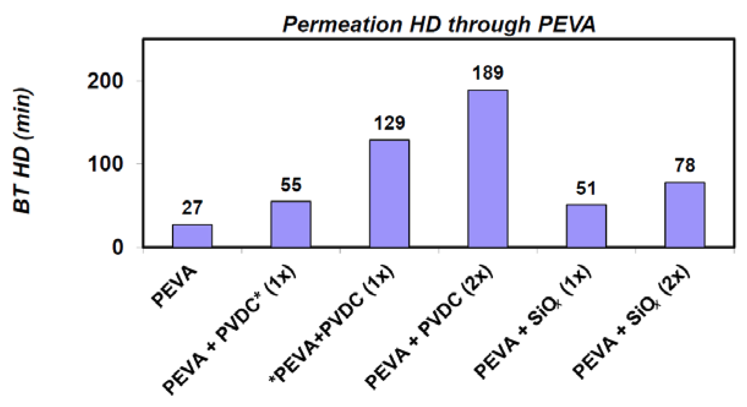
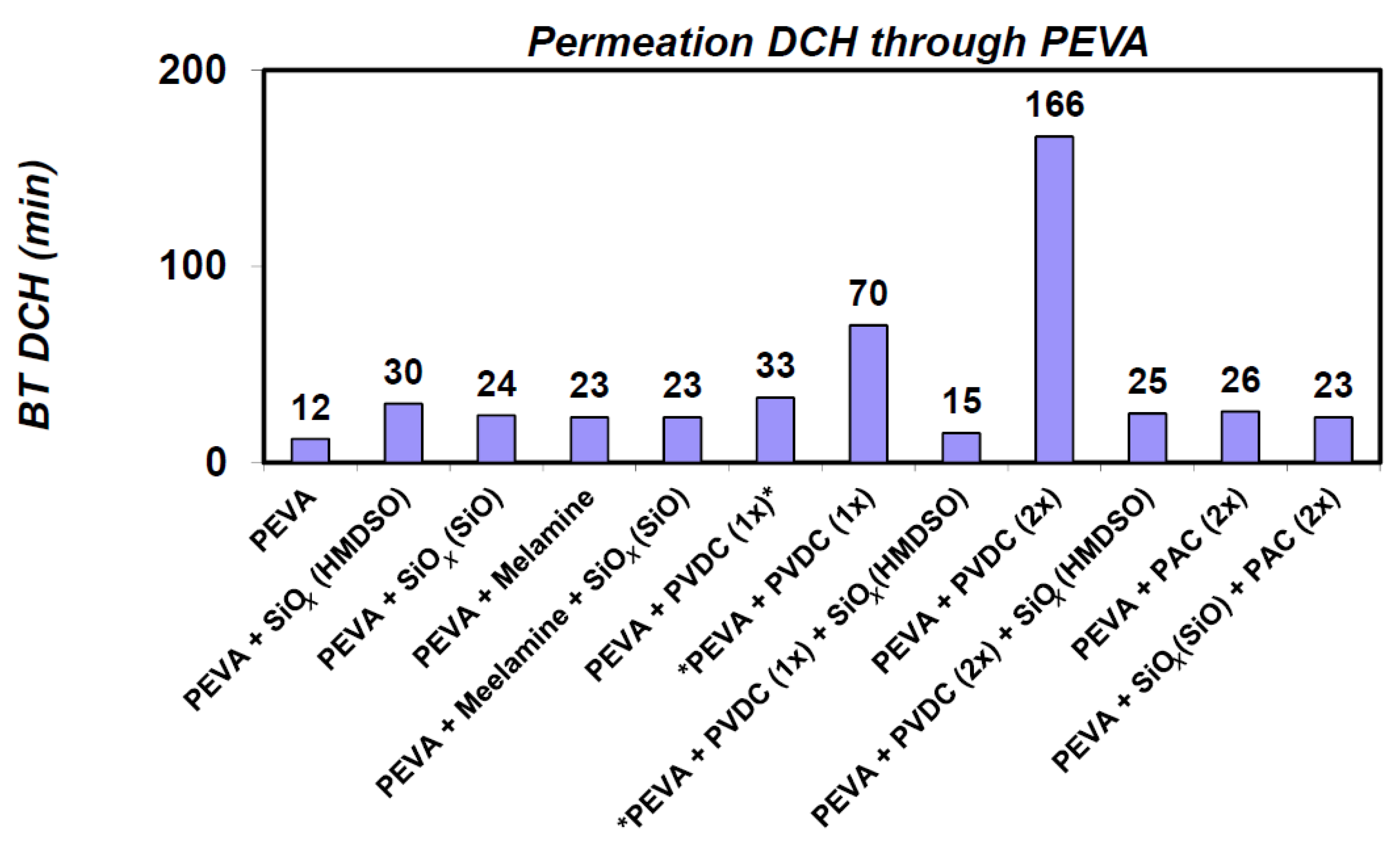
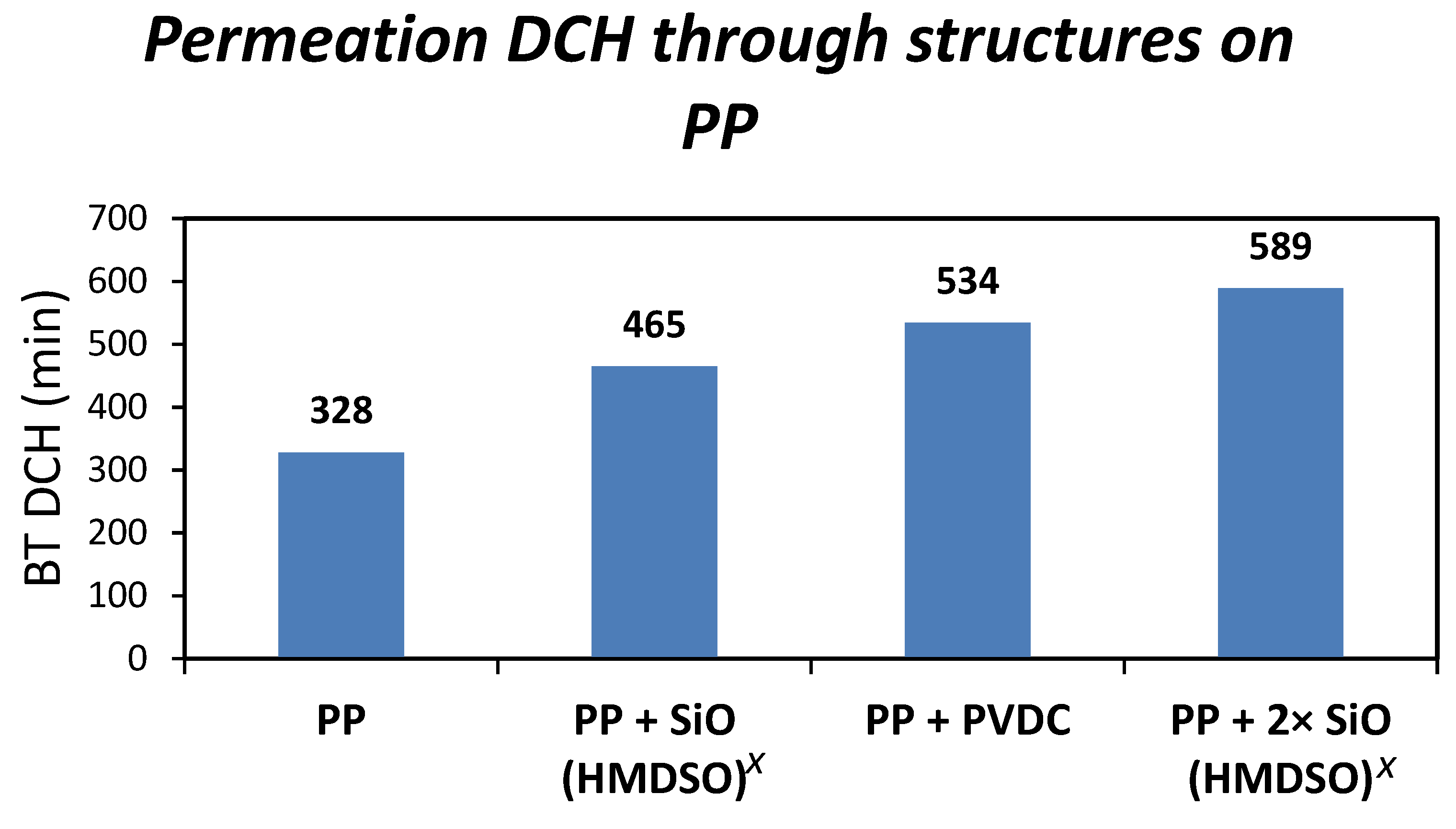
3.1. Protective Properties
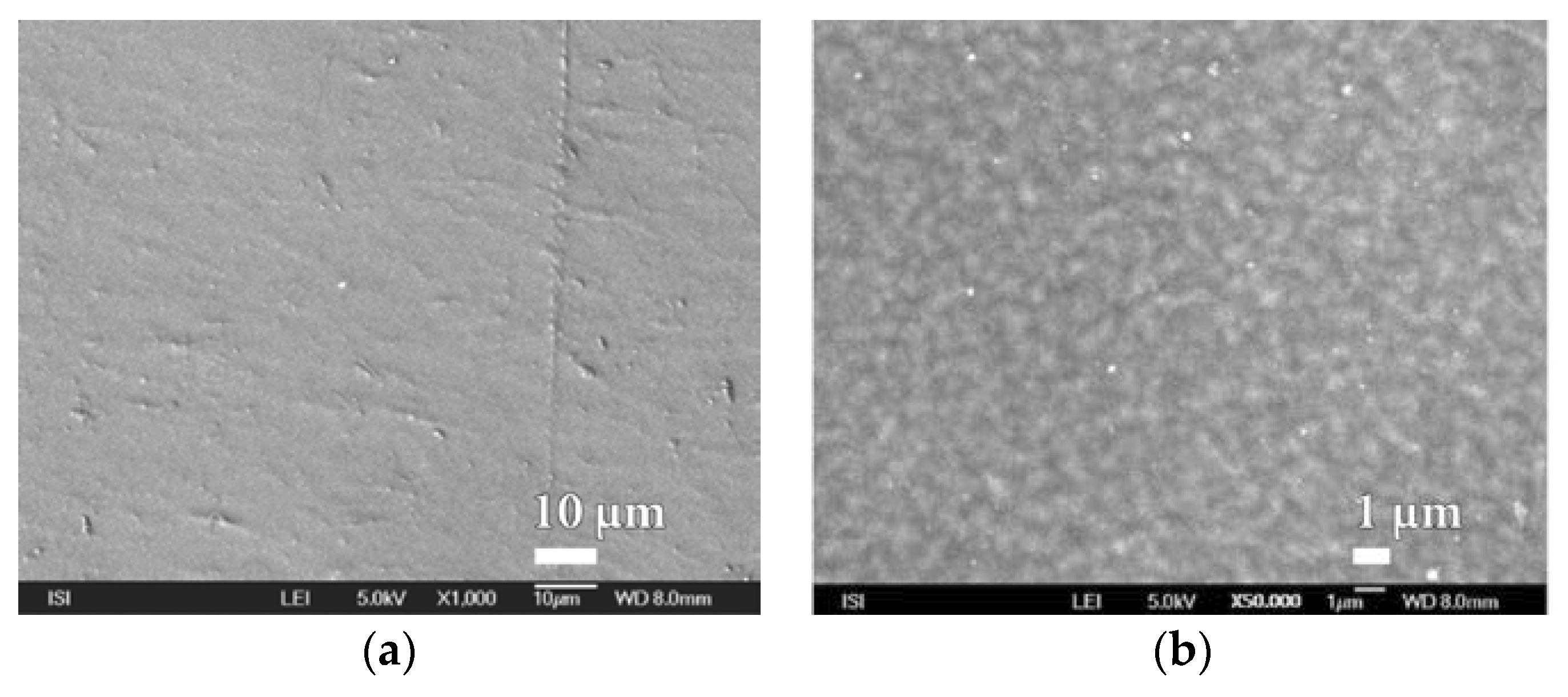
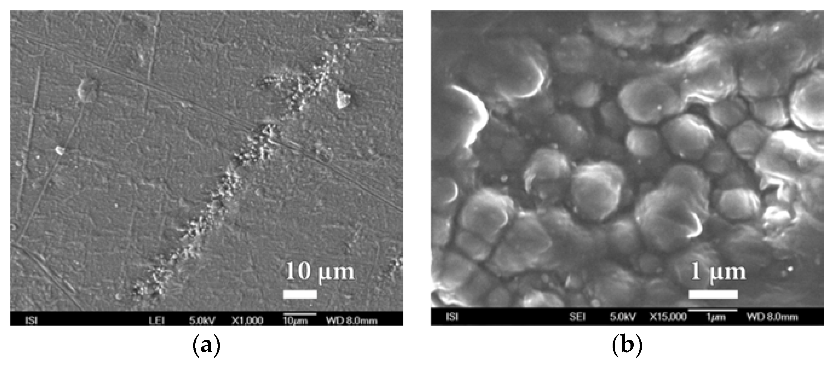
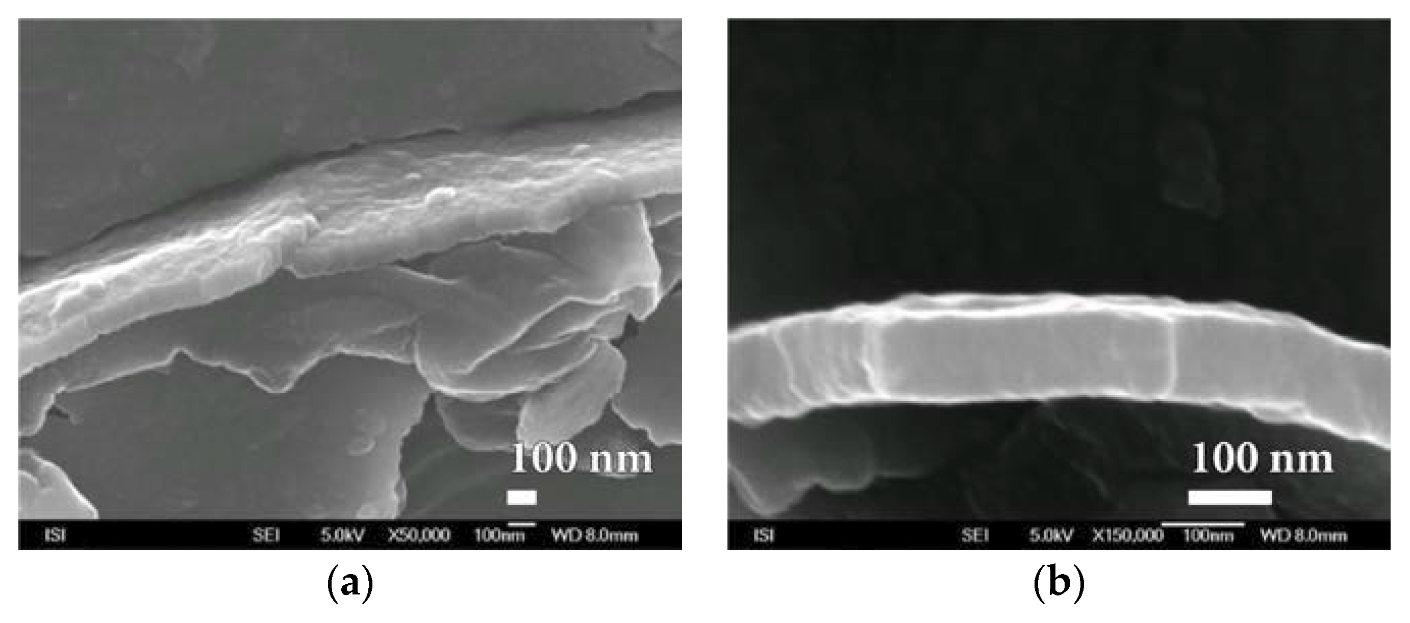
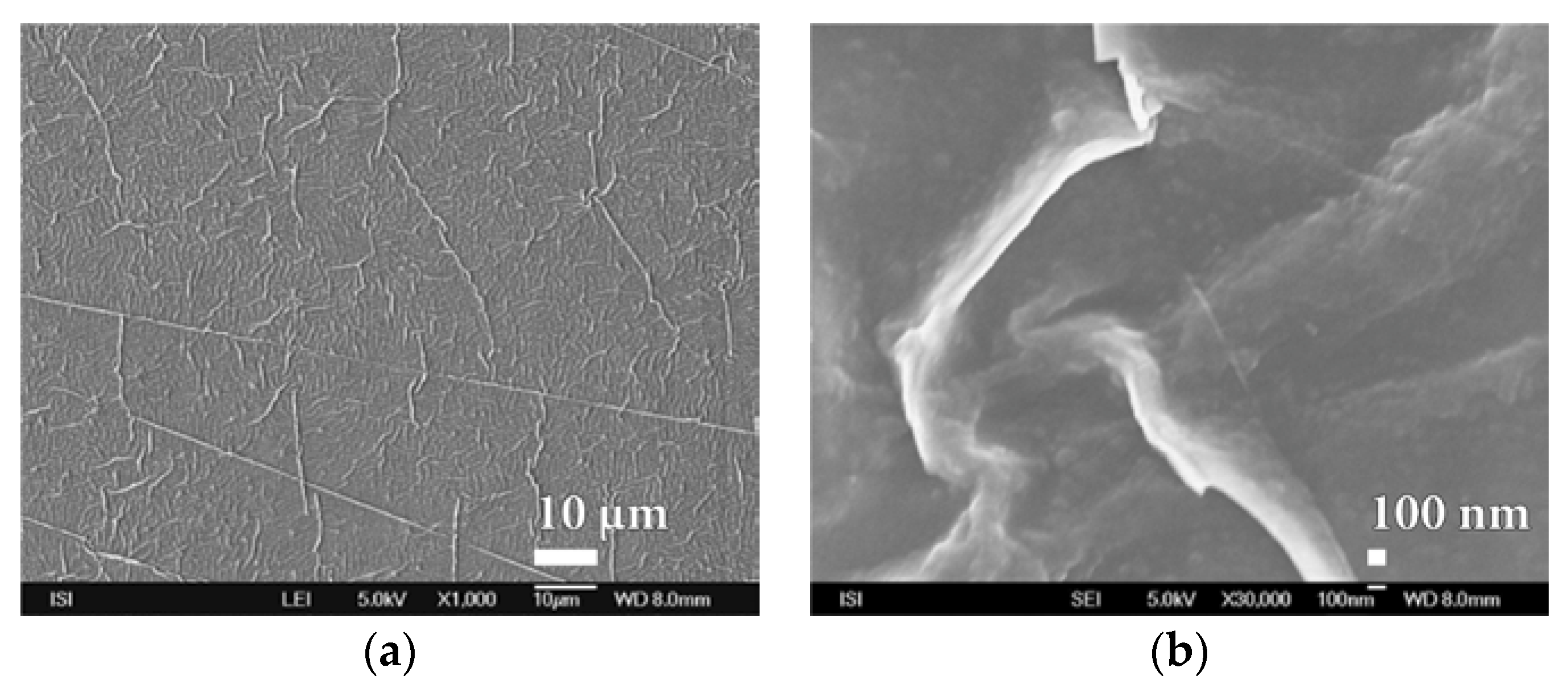
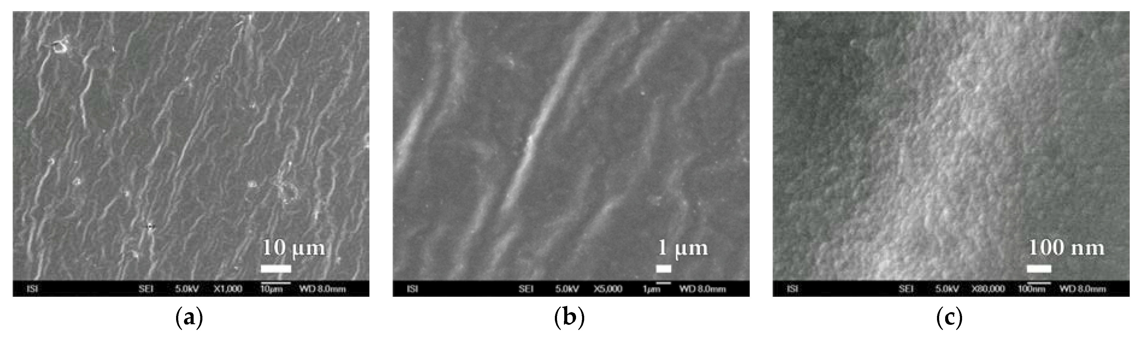
As a carrier material for barrier layers, PEVA has been used as a representative of an easily swellable polymer and PP as a representative of a low swellable polymer. Barrier layers of melamine, parylene, PVDC and SiOx have been applied to them occasionally combined with each other [25]. The prepared samples have been evaluated from the point of view of protective properties, microstructure and behaviour when exposed to the liquid phase of the test chemical. The PET foil is not suitable as the carrier material; otherwise testing the protective properties would be unbearably long.
Combinations of PEVA material with layers of parylene (by CVD), PVDC (by lamination) and SiOx (PE-CVD) have been prepared and evaluated. Due to the low protection properties of PEVA foil itself against liquid toxic substances, in our case, sulphur mustard (HD) and 1,6-dichlorohexane (DCH), the protective properties of these materials have been verified within one and both-sides coating with a thin layer of PVDC and SiOx. For one-sided coating, the PVDC has a breakthrough time value (BTY) of 55 min and 129 min from the site of PEVA. This difference has been caused due to the presence of the directional effect of permeation caused by the different swell ability of both materials. The PEVA foil itself had the RDY only 27 min. For both-sided PVDC lamination, BTY was found to be 188 min on one side and the second side. For DCH, these values are slightly lower and approximately equal to 51 min on PEVA side and 78 min on both sides covering from both sides (Figure 2).
Further combinations of PEVA foil with barrier layers of SiOx (by PE-CVD or PA-PVD), melamine (by PVD) and PVDC (by lamination) have been prepared [26,27]. These have been subsequently evaluated for resistance against the permeation of DCH. Interestingly, the resulting BT values for DCH in most combinations have been approximately the same and ranged from 23 to 33 min. The exception was only a combination with PVDC, with a single-sided coverage of BT 70 min from the PEVA side and 166 min with double-sided coverage. These results indicate that the exposure to DCH results in the rapid destruction of most barrier layers as a result of swelling of the carrier polymer so that the resulting protective properties of the starting material do not increase too much (Figure 3). The change in microstructure of the barrier layers following the DCH exposure described below also corresponds to these considerations.
In order to remove the impact of the swelling on the protective properties of the studied barrier layers, polypropylene has been used as the carrier polymer. The results shown in Figure 4 confirm previous considerations of the negative effect of the swelling of the carrier polymer on the protective properties of the applied barrier nanolayers.
A similar situation occurs when assessing the protective properties with the help of oxygen permeation (OTR), which also does not come to swelling of the carrier polymer (Figure 5).

3.2. Microstructure

The analysis is mainly focused on microstructure assessment of inorganic nanocoatings SiOx, which, when exposed to liquid test chemicals, unlike organic nanocoatings, resulted in significant destruction due to swelling of the polymer matrix. From a large number of SEM micrographs have been selected primarily those that were typical for the studied material and regularly repeated on different samples. Within large magnification, most researched SiOx layers were found to have characteristic granular substructures of tens of nanometres dimensions, which are the basic building blocks of these nanocoatings.
It is necessary to realize that within the plasma deposition of nanostructured SiOx barrier layers is a key parameter their elasticity and ductility, which usually is not more than 3% [27,28]. With gradual deformation of the substrate, the effect of ductility on protective properties can also be evaluated by OTR measurements, as there is no swelling of the carrier polymer which causes cracking and thus deterioration of the protective properties. When exposed to a liquid test chemical, the evaluation of the quality of the barrier layers is strongly dependent on the properties of the carrier substrate [29,30]. If a polymer resistant to swelling is used, the results of the protective properties evaluation are similar to those of the OTR. When using an easily swellable polymer, the cracks and defects in the barrier layer polymer are rapidly contaminated by the liquid test chemical and the subsequent swelling causes further destruction of the barrier layer and thereby deterioration of the protective properties.
However, the thickness of the barrier layer is also a crucial parameter. Basically, all publications dealing with the effect of the SiOx nanocoating thickness on barrier properties indicate an optimum where OTR values are best. The principle of thickness dependence on OTR is explained by the fact that in the nucleation area the discrete centres are first formed on the polymer substrate. The best OTR values are then achieved when they are interconnected. However, if a uniform nanolayer is rapidly formed in another region, its thickness is preferably increased and the growth of discontinuous centres is slowed down. However, a faster increase of the thickness of the barrier nanolayer at these sites above the optimum value, however, results in microcracks resulting from internal stress in the layer material which getting the OTR value worse.
As a basic comparison layer, a nanostructured SiOx layer on the silicon substrate has been prepared by PECVD by plasma deposition. It is apparent from Figure 6 and Figure S6 that the prepared nanocoating is homogeneous with a uniform microstructure that does not change even after prolonged exposure to DCH.
When assessing the quality of the SiOx nanocoatings, the surface quality of the carrier polymer foil should be taken into account in order to determine if found defects do not copy the underlying material. Figure 7 and Figure S7 shows the typical non-homogeneity of the surface of the PEVA foil to be taken into account when assessing the microstructure of SiOx nanocoatings.
For this reason, efforts were made to optimize plasma deposition conditions in order to improve the surface homogeneity of the polymer film used. One from the options was to modify the polymer matrix for less swelling. After verifying a number of PEVA surface treatment options, it was finally chosen to laminate it (at 110 °C without the binder) with a thin PVDC foil that showed good adhesion to the material. Another option was to replace the PEVA foil with a less-swelling PP film with a better surface. The use of PET foil that would be most suitable for plasma barrier coating was problematic because we could not measure too high BT values changes in protective properties in real time after applying different barrier layers. Polymeric matrices thus prepared were subjected to SiOx barrier nanocoatings with plasma deposition. Prepared samples have been evaluated not only from the point of permeation resistance and for microstructure of barrier nanocoatings surface before and after exposure of the DCH test chemical with high resolution SEM. It is evident from Figure 8 and Figure S8 that the quality of the PVDC surface is significantly better than the original PEVA foil. It has been shown that this material is not porous even at high magnification (80,000×) and therefore it can be advantageously used for the deposition of other barrier layers based on melamine, parylene and mainly SiOx plasma technology.
However, it is interesting to note that even with short-term oxygen plasma treatment, the surface of the PVDC foil is significantly wrinkled, while its homogeneity remains unchanged (Figure 9 and Figure S9).
A homogeneous layer of SiOx with a well-developed microstructure which is probably very thin is formed with plasma deposition by PVD method on the surface of the PVDC foil (Figure 10 and Figure S10).
Similarly, within plasma deposition with the PVD method, at this time on the surface of PEVA foil, behaves even melamine and parylene C. The characteristic microstructure of the surface of these barrier nanocoatings is shown in Figure 11 and Figure 12. In both cases a compact and fairly homogeneous barrier nanocoating with a well-developed microstructure copying the PEVA foil surface is formed. A comparison of the microstructures in Figure 10, Figure 11 and Figure 12 and Figure S10–S12 show that melamine produces a coarser microstructure than SiOx but thicker than parylene C. Further SiOx nanocoatings on PEVA film have been prepared by plasma deposition with the HMDSO method. Within this method of preparation, it is possible, in accordance with conditions during exposure, to form a SiOx nanocoating of the different character than within plasma deposition by PVD method.
The different appearance of SiOx nanocoatings prepared under various experimental conditions, documented in Figure 13 and Figure S13, is probably related to the nanocoating thickness and properties of the carrier substrate.
This assumption confirms the deposition of SiOx by the HMDSO method on the silicon wafer surface, documented in Figure 14 and Figure S14.
The SiOx nanocoating has been deposited on the surface of the Viton elastomer by the HMDSO method for comparison, documented in Figure 15 and Figure S15. Interestingly, in this case a homogeneous barrier layer has been formed, however with a porous microstructure.
The nanocoating SiOx has been deposited on the surface of both PP and PET foils by the HMDSO method. The formed nanocoating has been both nonporous and homogeneous with a well-developed microstructure copying the surface of the PP foil, as shown in Figure 16.
If samples of polymeric materials with a SiOx barrier layer are exposed to liquid DCH, an easily swellable PEVA polymer matrix will dramatically change the appearance of this nanocoating. Liquid DCH permeating through micro cracks or other leaks to the polymeric matrix apparently will not prevent its rapid swelling which causes destruction of the SiOx nanopowder [30,31,32]. This effect will not appear at all or only to a small extent in the scope of PP foils or PET foils. It is conformable with the discussion above related to the protective properties of these materials. The destruction of the SiOx barrier layer due to the polymer matrix embossment can be demonstrated by many of the examples shown in Figure S4. However, visual changes due to the polymer matrix swelling from visual changes due to mechanical damage to the SiOx barrier layer, as documented in Figure S5, are required.
During the study of SiOx nanocoatings after destruction, sites with such great damage have been found. It was possible to precisely determine the thickness of deposited barrier layer moving around 100 nm (Figure 17 and Figure S16). It even appears that in some cases the SiOx nanocoating has a multilayer character of approximately 100 nm (Figure 17a).
Another interesting finding is the typical spherical substructure characteristic of most studied SiOx nanocoatings. This substructure, clearly recognizable only with sufficiently large magnification, is also found inside deep material defects and even creates interesting structures on the surface and on the smooth surface of the PEVA foil, as can be seen from Figure 18.

4. Conclusions

It has been shown that the plasma deposition in vacuum can form barrier nanopowders from SiOx and other suitable substrates on the polymer matrix. It is clear from the results that the HMDSO method, which makes it possible to influence the SiOx nanocoating thickness and quality better, is more appropriate. Within forming practically applicable barrier materials with nanocoating of SiOx it is necessary to be respect several essential requirements. The nanocoating SiOx must be deposited primarily on a low swellable polymeric foil and, due to its brittleness, it must immediately be laminated with another foil due to prevention of its mechanical damaged. This is in a harmony with the production process of ALCAN Company within the production of packaging with barrier properties of CERAMIS® technology. The aim of further research in this field should be to improve the fixation of barrier nanocoatings on the polymer matrix and their resistance to mechanical stress. If it is real to prepare reactive coatings or deposition of suitable metallic oxides with catalytic properties it would enable this process to be used for the preparation of nanocoatings and nanomaterials with self-decontaminating or photocatalytic properties during further research.

Supplementary Materials

The following are available online at https://www.mdpi.com/2079-4991/8/9/679/s1, Figure S1: The principle of CERAMIS® reactive steam technology and examples of SiOx® coated materials, Figure S2: The scheme of the PE-CVD/PA-PVD apparatus for the preparation of SiOxnanocoatingsSiOx with steaming form powder SiO in vacuum, Figure S3: Diagram and real appearance of the SorpTest device for testing the resistance of barrier materials against the permeation of gaseous and liquid toxic substances, Figure S4: Scanning electron microscopy (SEM) micrographs of examples of visual changes of the SiOx barrier layer caused by polymer matrix swelling with visible different kinds of cracks, Figure S5: Scanning electron microscopy (SEM) micrographs of examples of visual changes of the SiOx barrier layer caused by mechanical damage, Figure S6: Scanning electron microscopy (SEM) micrographs of the surface of the nanolayer of SiOx prepared by HMDSO method on the silicon substrate at various magnifications of 20,000× before exposure to DCH, Figure S7: The exhibitions of different inhomogeneity on the surface of the used polymer foil PEVA at various magnification of (a) 30,000×, (b) 15,000×, (c) 80,000×, Figure S8: SEM micrographs of PVDC foil surface laminated at 110 °C to PEVA foil at magnification of 30,000×, Figure S9: SEM micrographs of PVDC foil surface laminated to PEVA foil after short exposure to oxygen plasma treatment at magnification of 5000, Figure S10: SEM micrographs of the surface SiOx barrier nanocoating prepared by plasma deposition with the PVD method on PVDC foil laminated on the PEVA foil, at magnification of 5000×, Figure S11: SEM micrographs of melamine nanocoating surface on PEVA SiOx foil prepared by PVD plasma deposition method at magnification of 30,000×, Figure S12: SEM micrographs of parylenenanocoating surface on PEVA SiOx foil prepared by PVD plasma deposition method at magnification of 5000×, Figure S13: SEM micrographs of SiOx barrier nanocoating surface prepared by the plasma deposition by HMDSO method on PEVA foil at magnification of (a) 1000× and on PEVA foil stained with aluminium at magnification (b) 1000×, Figure S14: SEM micrographs of surface SiOx barrier nanocoating prepared by plasma deposition by HMDSO on the silicon wafer at magnification of 1000×, Figure S15: SEM micrographs of surface SiOx barrier nanocoating prepared by plasma deposition by HMDSO method on the Viton fluorelastomer at magnification of 5000×, Figure S16: SEM photographs of SiOx barrier nanocoating fracture prepared by plasma deposition by HMDSO method on PEVA foil at magnification of 100,000×.

Author Contributions

Conceptualization, P.O. and V.O.; Methodology, P.O. and V.O.; Validation, R.P., P.O., V.O. and R.K.; Formal Analysis, R.P., P.O., V.O and L.S.; Investigation, P.P., V.O., L.S., R.K. and J.B.; Resources, R.P., V.O., R.K. and J.B.; Data Curation, R.P., P.O., V.O and L.S.; Writing-Original Draft Preparation, P.O. and V.O.; Writing-Review & Editing, P.O. and R.P.; Supervision, P.O. and R.P; Project Administration, P.O. and V.O.; Funding Acquisition, R.P.

Funding

This work was supported by Czech Ministry of Education, Youth and Sports, Project number LO1211, Material Research Centre at Faculty of Chemistry, Brno University of Technology.

Acknowledgments

We would like to thank all subjects who volunteered in the study.

Conflicts of Interest

The authors declare no conflict of interest.

References

  1. Kogelschatz, U.; Eliasson, B.; Egli, W. Dielectric-barrier discharges principle and applications. J. Phys. Arch. 1997, 7, C4-47–C4-66. [Google Scholar] [CrossRef]
  2. Otrisal, P.; Florus, S.; Svorc, L.; Barsan, G.; Mosteanu, D. A new colorimetric assay for determination of selected toxic vapours and liquids permeation through barrier materials using the minitest device. Rev. Plast. 2017, 54, 748–751. [Google Scholar]
  3. Kmochova, A.; Tichy, A.; Zarybnicka, L.; Sinkorova, Z.; Vavrova, J.; Rehacek, V.; Durisova, K.; Kubelkova, K.; Pejchal, J.; Kuca, K. Modulation of ionizing radiation-induced effects by NU7441, KU55933 and VE821 in peripheral blood lymphocytes. J. Appl. Biomed. 2016, 14, 19–24. [Google Scholar] [CrossRef]
  4. Krumpolec, R.; Zahoranova, A.; Cernak, M.; Kovacik, D. Chemical and physical evaluation of hydrophobic pp-HMDSO layers deposited by plasma polymerization at atmospheric pressure. Chem. Listy 2012, 106, 1450–1454. [Google Scholar]
  5. Radovan, K.M.; Negovan, I.D.; Dalibor, J.B.; Smiljana, M.M.; Dejan, I.R.; Marija, M.D.; Branko, K.V. Dynamic adsorption characteristics of thin layered activated charcoal materials used in chemical protective overgarments. Indian J. Fibre Text. Res. 2016, 41, 402–410. [Google Scholar]
  6. Mosteanu, D.; Barsan, G.; Otrisal, P.; Giurgiu, L.; Oancea, R. Obtaining the volatile oils from wormwood and tarragon plants by a new microwave hydrodistillation method. Rev. Chim. 2017, 68, 2499–2502. [Google Scholar]
  7. Sun, Y.J.; Fu, Y.B.; Chen, Q.; Zhang, C.M.; Sang, L.J.; Zhang, Y.F. Silicon dioxide coating deposited by PDPs on PET films and influence on oxygen transmission rate. Chin. Phys. Lett. 2008, 25, 1753–1756. [Google Scholar]
  8. Felts, J.T. Transparent barrier coatings update: Flexible substrates. J. Plast. Film. Sheeting 1993, 9, 139–158. [Google Scholar] [CrossRef]
  9. Macák, J.M.; Hromádko, L.; Bulánek, R.; Koudelková, E.; Buk, J.; Tejkl, M. Process for Preparing Submicron Fibers of Amorphous Silica and Submicron Fibers of Amorphous Silica Prepared in Such a Manner. Available online: https://1url.cz/qtyDc (accessed on 12 June 2018).
  10. Madocks, J.; Marcus, P.; Morse, P. Silicon dioxide coatings on plastic substrates by large area plasma enhanced chemical vapour deposition process. In Proceedings of the 49th Annual Technical Conference, Washington, DC, USA, 22–27 April 2006; pp. 569–573. [Google Scholar]
  11. Hoskova-Mayerova, S.; Maturo, A. Algebraic hyperstructures and social relations. Italian J. Pure. Appl. Math. 2018, 39, 701–709. [Google Scholar]
  12. Anonymous. CERAMIS® Barrier Films: Transparent SiOx Barrier Films for Ultimate Product Protection. Available online: https://1url.cz/Pt734 (accessed on 23 June 2018).
  13. Roberts, A.P.; Henry, B.M.; Sutton, A.P.; Grovenor, C.R.M.; Briggs, G.A.D.; Miyamoto, T.; Kano, M.; Tsukahara, Y.; Yanaka, M. Gas permeation in silicon-oxide/polymer (SiOx/PET) barrier films: Role of the oxide lattice, nano-defects and macro-defects. J. Membr. Sci. 2002, 208, 75–88. [Google Scholar] [CrossRef]
  14. Erlat, A.G.; Spontak, R.J.; Clarke, R.P.; Robinson, T.C.; Haaland, P.D.; Tropsha, Y.; Harvey, N.G.; Vogler, E.A. SiOx gas barrier coatings on polymer substrates:  Morphology and gas transport considerations. J. Phys. Chem. B 1999, 103, 6047–6055. [Google Scholar] [CrossRef]
  15. Felts, J.; Finson, E.J. Transparent SiO2 barrier coatings: Conversion and production status. In Proceedings of the 37th Annual Technical Conference Proceedings, Boston, MA, USA, 8–13 May1994; pp. 139–143. [Google Scholar]
  16. Foest, R.; Schafer, J.; Quade, A.; Ohl, A.; Weltmann, K.D. Miniaturized atmospheric pressure plasma jet (APPJ) for deposition of SiOx films with different Silicon-organics compounds—A comparative study. In Proceedings of the 35th EPS Conference on Plasma Phys, Hersonissos, Greece, 9–13 June 2008. [Google Scholar]
  17. Gaur, S.; Vergason, G. Plasma polymerization: For industrial production. In Proceedings of the 44th Annual Technical Conference Proceedings, Philadelphia, PA, USA, 21–26 April 2001. [Google Scholar]
  18. Huang, X. Fabrication and Properties of Carbon Fibers. Materials 2009, 1, 938–947. [Google Scholar] [CrossRef]
  19. Horova, I.; Kolacek, J.; Vopatova, K. Full bandwidth matrix selectors for gradient kernel density estimate. Comput. Stat. Data Anal. 2013, 57, 364–376. [Google Scholar] [CrossRef]
  20. Raynaud, P.; Clergereaux, R.; Segui, Y.; Gherardi, N.; Despax, B. Plasma Nanolayering, Nanoclustering, Nanotexturing: Challenges for Future Processes for Mass Produstion. Available online: https://1url.cz/Yt73j (accessed on 23 June 2018).
  21. Starostin, S.A.; Aldea, E.; Vries, H.W.; Creatore, M.; van de Sanden, M.C.M. Application of atmospheric pressure glow discharge (APGD) for deposition of thin silica like films on polymeric webs. In Proceedings of the 28th International Conference on Phenomena in Ionized Gases (ICPIG), Prague, Czech Republic, 15–20 July 2007. [Google Scholar]
  22. Fortin, J.B.; Lu, T.-M. Chemical Vapor Deposition Polymerization: The Growth and Properties of Parylene Thin Films; Springer Science & Business Media: New York, NY, USA, 2003. [Google Scholar] [CrossRef]
  23. Gorham, W.F. A new, general synthetic method for the preparation of linear poly-p-xylylenes. J. Polym. Sci. Part A 1966, 4, 3027–3039. [Google Scholar] [CrossRef]
  24. Míša, M.; Obšel, V. System for Measuring Permeation of Gases and Vapors Through Barrier Membranes. Available online: https://1url.cz/Bty4h (accessed on 11 June 2018).
  25. Yasuda, H. Plasma Polymerization; 1st Issue; Academic Press: Orlando, FL, USA, 1985. [Google Scholar]
  26. Smith, A.W.; Copeland, N. Clear barrier coatings by plasma CVD for packaging applications. In Proceedings of the 43th Annual Technical Conference Proceedings, Washington, DC, USA, 22–27 April 2006; pp. 636–641. [Google Scholar]
  27. Izu, M.; Dotter, B.; Ovshinsky, S.R. Roll-to-roll microwave PECVD machine for high-barrier film coatings. J. Photopolym. Sci. Technol. 1995, 8, 195–204. [Google Scholar] [CrossRef]
  28. Hones, P.; Levy, F.; Randall, N.X. Influence of deposition parameters on mechanical properties of sputter-deposited Cr2O3 thin films. J. Mater. Res. 1999, 14, 3623–3629. [Google Scholar] [CrossRef]
  29. Jahromi, S.; Moosheimer, S.U. Oxygen barrier coatings based on supramolecular assembly of melamine. Macromolecules 2002, 33, 7582–7587. [Google Scholar] [CrossRef]
  30. Howells, D.G.; Henry, B.M.; Leterrier, Y.; Manson, J.A.E.; Madocks, J.; Assender, H.E. Mechanical properties of SiOx gas barrier coatings on polyester films. Surf. Coat. Technol. 2008, 202, 3529–3537. [Google Scholar] [CrossRef]
  31. Ozeki, K.; Nagashima, Y.; Ohgoe, Y.; Hirakuri, K.K.; Mukaibayashi, H.; Masuzawa, T. Gas barrier properties of diamond-like carbon films coated on PTFE. Appl. Surf. Sci. 2009, 25, 7286–7290. [Google Scholar] [CrossRef]
  32. Stodola, P. Using metaheuristics on the multi-depot vehicle routing problem with modified optimization criterion. Algorithms 2018, 11, 74. [Google Scholar] [CrossRef]
Figure 1. Influence of the barrier nanolayers arrangement on the protective properties of polymeric barrier materials.
Nanomaterials 08 00679 g001
Figure 2. Breakthrough times of modifiedpolyethylenevinyl acetate (PEVA) foil determinate by the MikroTest method.
Nanomaterials 08 00679 g002
Figure 3. The resistance of the PEVA foil modified with different barrier layers against 1,6-dichlorohexane (DCH).
Nanomaterials 08 00679 g003
Figure 4. Resistance of the PP foil modified with different barrier layers against DCH permeation.
Nanomaterials 08 00679 g004
Figure 5. Oxygen permeation values detected for PEVA foil with barrier layers of PVDC, plasma polymerized HMDSO and parylene.
Nanomaterials 08 00679 g005
Figure 6. Scanning electron microscopy (SEM) micrographs of the surface of the nanolayer of SiOx prepared by HMDSO method on the silicon substrate at various magnifications before exposure to DCH (a) 1000× and (b) 50,000×.
Nanomaterials 08 00679 g006
Figure 7. The exhibitions of different inhomogeneity on the surface of the used polymer foil PEVA at various magnifications of (a) 10,000×; (b) 30,000×;(c) 5000×.
Nanomaterials 08 00679 g007
Figure 8. SEM micrographs of PVDC foil surface laminated at 110 °C to PEVA foil at magnification of (a) 1000× and (b) 80,000×.
Nanomaterials 08 00679 g008
Figure 9. SEM micrographs of PVDC foil surface laminated to PEVA foil after short exposure to oxygen plasma treatment at magnification of (a) 1000× (b) 30,000×.
Nanomaterials 08 00679 g009
Figure 10. SEM micrographs of the surface SiOx barrier nanocoating prepared by plasma deposition with the PVD method on PVDC foil laminated on the PEVA foil, at magnification of (a) 1000× and (b) 80,000×.
Nanomaterials 08 00679 g010
Figure 11. SEM micrographs of melamine nanocoating surface on PEVA SiOx foil prepared by PVD plasma deposition method at magnification of (a) 250× and (b) 100,000×.
Nanomaterials 08 00679 g011
Figure 12. SEM micrographs of parylene nanocoating surfaces on PEVA SiOx foil prepared by PVD plasma deposition method at magnification of (a) 1000× and (b) 15,000×.
Nanomaterials 08 00679 g012
Figure 13. SEM micrographs of SiOx barrier nanocoating surface prepared by the plasma deposition by HMDSO method on PEVA foil at magnification of (a) 5000× and (b) 100,000× and on PEVA foil stained with aluminium at magnification of (c) 50× and (d) 300×.
Nanomaterials 08 00679 g013
Figure 14. SEM micrographs of surface SiOx barrier nanocoating prepared by plasma deposition by HMDSO on the silicon wafer at magnification of (a) 300× and (b) 1000×.
Nanomaterials 08 00679 g014
Figure 15. SEM micrographs of surface SiOx barrier nanocoating prepared by plasma deposition by HMDSO method on the Viton fluorelastomer at magnification of (a) 250× and (b) 80,000×.
Nanomaterials 08 00679 g015
Figure 16. SEM micrographs of SiOx barrier nanocoating surface prepared by plasma deposition by HMDSO method on the PP foil at magnification of (a) 1000×, (b) 5000× and (c) 80,000×.
Nanomaterials 08 00679 g016
Figure 17. SEM photographs of SiOx barrier nanocoating fracture prepared by plasma deposition by HMDSO method on PEVA foil at magnification of (a) 50,000× and (b) 150,000×.
Nanomaterials 08 00679 g017
Figure 18. SEM micrographs of SiOx nanocoating substructure prepared by plasma deposition by HMDSO method on the PEVA foil at magnification of 80,000× of three different areas. (a) Typical surface morphology; (b) layer defect and (c) surface abnormality.
Nanomaterials 08 00679 g018

