Fabrication of Durable Ordered Ta2O5 Nanotube Arrays Decorated with Bi2S3 Quantum Dots

 , , ,
, , ,  , and
, and
Abstract
:
1. Introduction
2. Materials and Methods
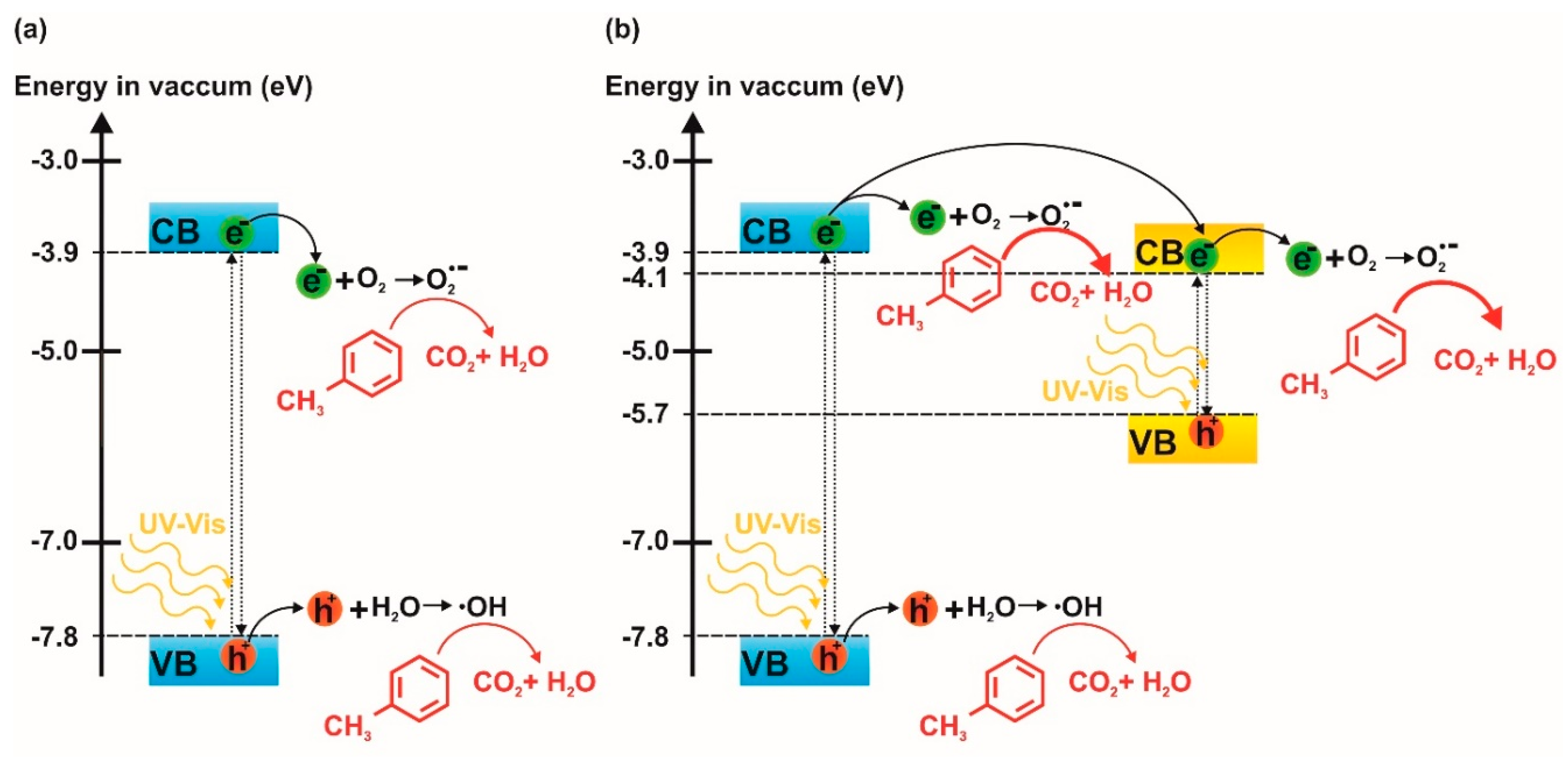
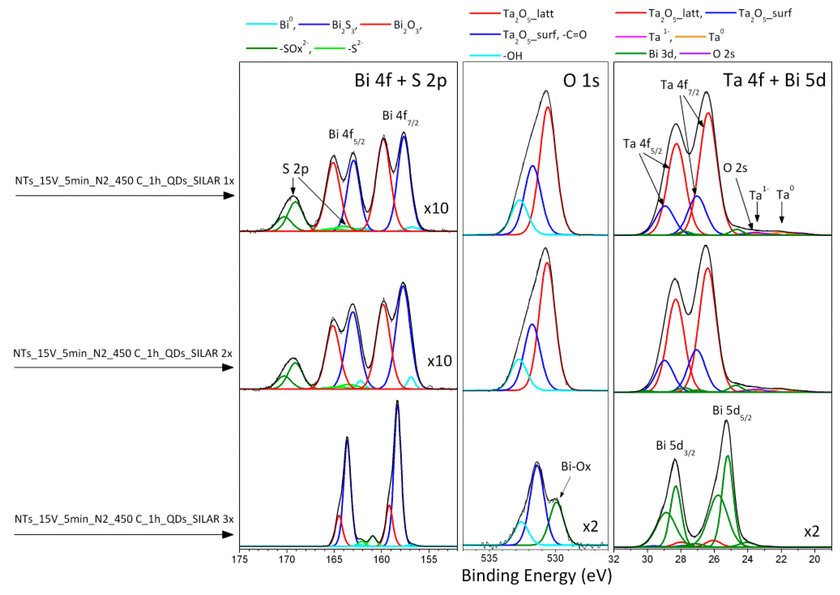
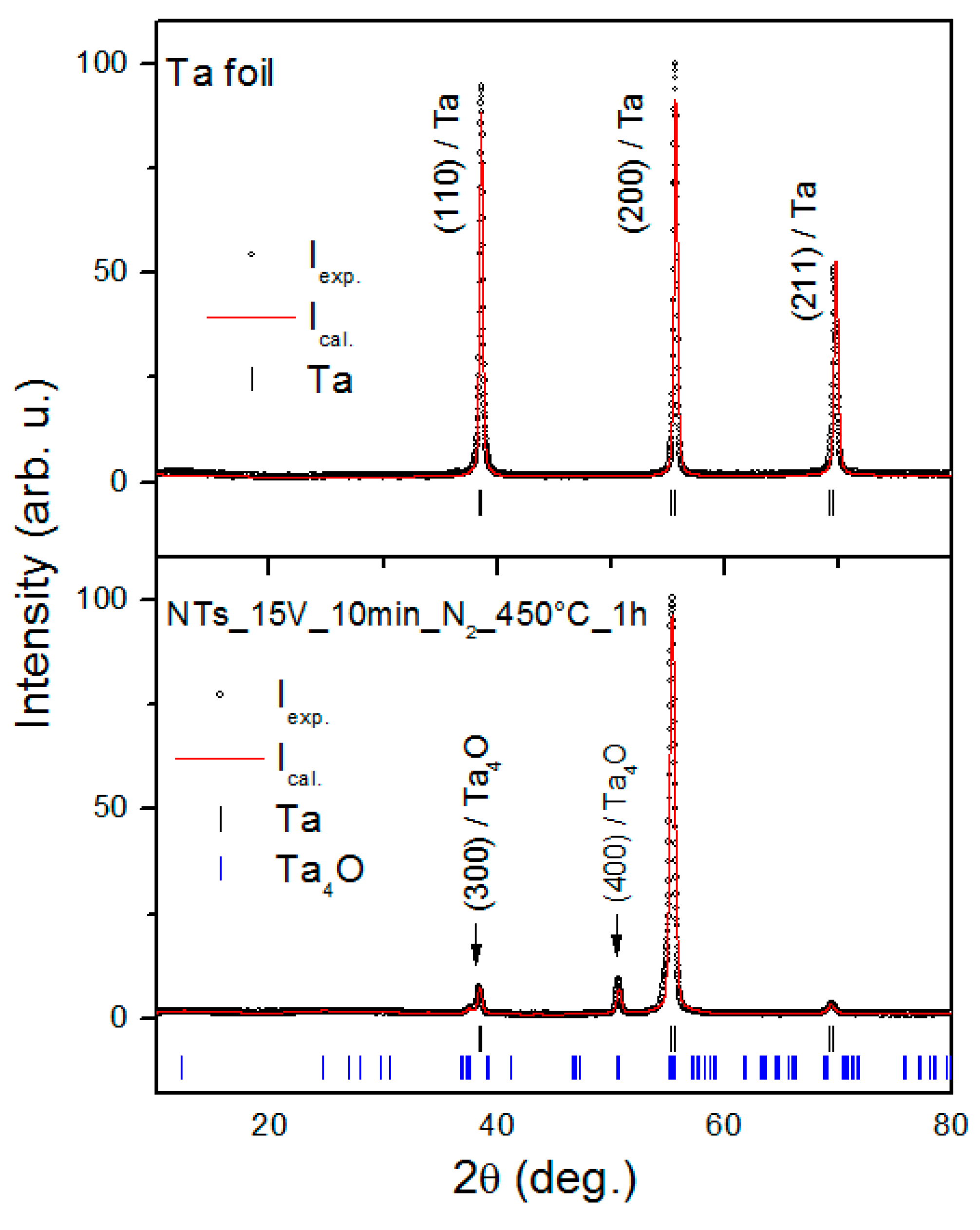
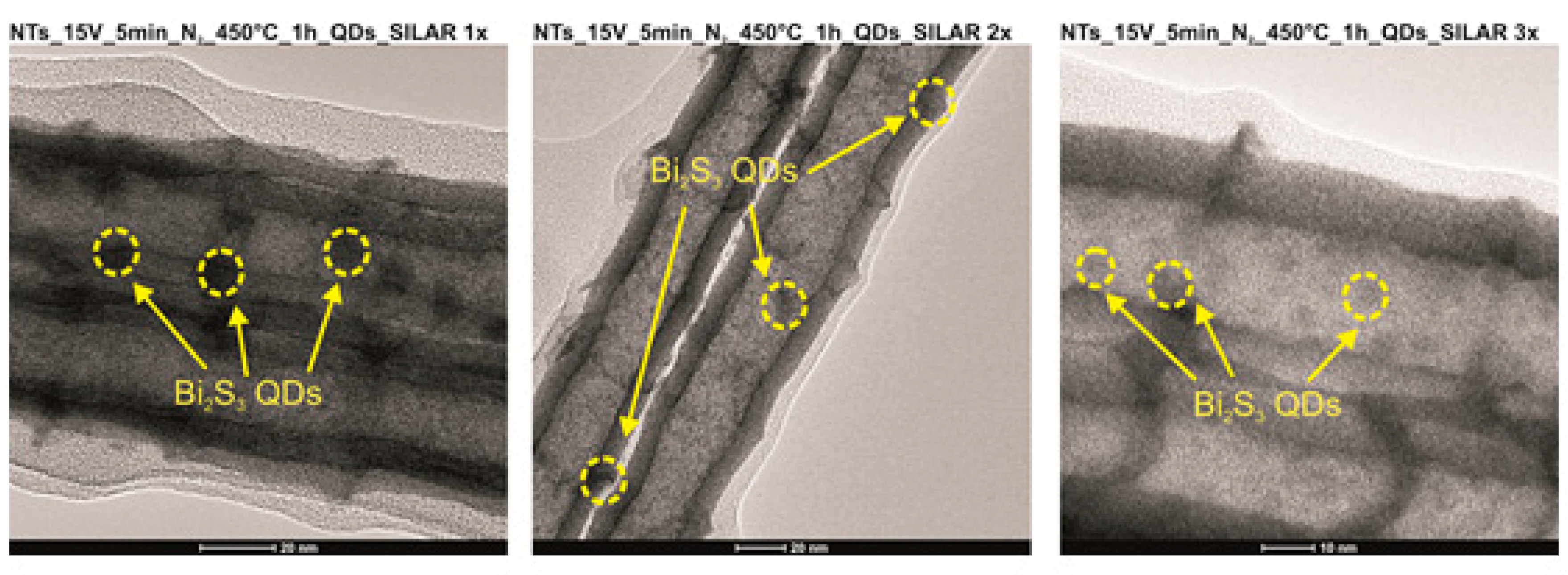
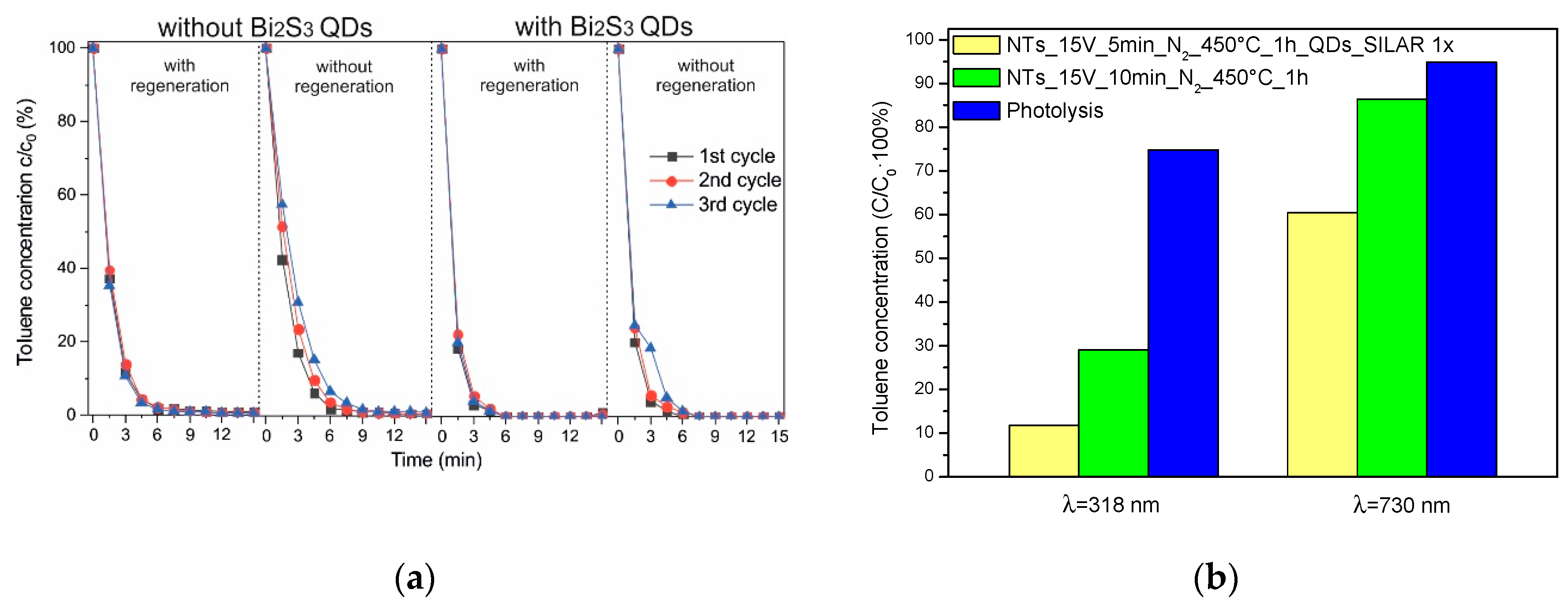
3. Results
4. Conclusions
Supplementary Materials
Author Contributions
Funding
Conflicts of Interest
References
- Colmenares, J.C.; Yi-Jun, X. Heterogeneous Photocatalysis; Springer: Berlin/Heidelberg, Germany, 2016. [Google Scholar]
- Hisatomi, T.; Kubota, J.; Domen, K. Recent advances in semiconductors for photocatalytic and photoelectrochemical water splitting. Chem. Soc. Rev. 2014, 43, 7520–7535. [Google Scholar] [CrossRef] [PubMed]
- Noda, Y.; Lee, B.; Domen, K.; Kondo, J.N. Synthesis of Crystallized Mesoporous Tantalum Oxide and Its Photocatalytic Activity for Overall Water Splitting under Ultraviolet Light Irradiation. Chem. Mater. 2008, 20, 5361–5367. [Google Scholar] [CrossRef]
- Li, J.; Dai, W.; Wu, G.; Guan, N.; Li, L. Fabrication of Ta2O5 films on tantalum substrate for efficient photocatalysis. Catal. Commun. 2015, 65, 24–29. [Google Scholar] [CrossRef]
- Gonçalves, R.V.; Migowski, P.; Wender, H.; Eberhardt, D.; Weibel, D.E.; Sonaglio, F.C.; Zapata, M.J.M.; Dupont, J.; Feil, A.F.; Teixeira, S.R. Ta2O5 Nanotubes Obtained by Anodization: Effect of Thermal Treatment on the Photocatalytic Activity for Hydrogen Production. J. Phys. Chem. C 2012, 116, 14022–14030. [Google Scholar] [CrossRef]
- Chaneliere, C.; Autran, J.L.; Devine, R.A.B.; Balland, B. Tantalum pentoxide (Ta2O5) thin films for advanced dielectric applications. Mater. Sci. Eng. R Rep. 1998, 22, 269–322. [Google Scholar] [CrossRef]
- Baltes, M.; Kyto, A.; Weckhuysen, B.M.; Schoonheydt, R.A.; Van Der Voort, P.; Vansant, E.F. Supported Tantalum Oxide and Supported Vanadia-tantala Mixed Oxides: Structural Characterization and Surface Properties. J. Phys. Chem. B 2001. [Google Scholar] [CrossRef]
- Azim, O.A.; Abdel-Aziz, M.M.; Yahia, I.S. Structure and optical analysis of Ta2O5 deposited on infrasil substrate. Appl. Surf. Sci. 2009, 255, 4829–4835. [Google Scholar] [CrossRef]
- Kesmez, Ö.; Akarsu, E.; Çamurlu, H.E.; Yavuz, E.; Akarsu, M.; Arpaç, E. Preparation and characterization of multilayer anti-reflective coatings via sol-gel process. Ceram. Int. 2018, 44, 3183–3188. [Google Scholar] [CrossRef]
- Ezhilvalavan, S.; Tseng, T.Y. Preparation and properties of tantalum pentoxide (Ta2O5) thin films for ultra large scale integrated circuits (ULSIs) application—A review. J. Mater. Sci. Mater. Electron. 1999, 10, 9–31. [Google Scholar] [CrossRef]
- Kato, H.; Asakura, K.; Kudo, A. Highly Efficient Water Splitting into H2 and O2 over Lanthanum-Doped NaTaO3 Photocatalysts with High Crystallinity and Surface Nanostructure. J. Am. Chem. Soc. 2003, 125, 3082–3089. [Google Scholar] [CrossRef]
- Duan, J.; Shi, W.; Xu, L.; Mou, G.; Xin, Q.; Guan, J. Hierarchical nanostructures of fluorinated and naked Ta2O5 single crystalline nanorods: Hydrothermal preparation, formation mechanism and photocatalytic activity for H2 production. Chem. Commun. 2012, 48, 7301. [Google Scholar] [CrossRef] [PubMed]
- Liu, J.; Wei, A.; Zhao, X.; Zhang, H. Structural and electrical properties of Ta2O5 thin films prepared by photo-induced CVD. Bull. Mater. Sci. 2011, 34, 443–446. [Google Scholar] [CrossRef]
- Lee, K.; Schmuki, P. Highly ordered nanoporous Ta2O5 formed by anodization of Ta at high temperatures in a glycerol/phosphate electrolyte. Electrochem. Commun. 2011, 13, 542–545. [Google Scholar] [CrossRef]
- Su, Z.; Grigorescu, S.; Wang, L.; Lee, K.; Schmuki, P. Fast fabrication of Ta2O5 nanotube arrays and their conversion to Ta 3 N 5 for efficient solar driven water splitting. Electrochem. Commun. 2015, 50, 15–19. [Google Scholar] [CrossRef]
- Kobylański, M.P.; Mazierski, P.; Malankowska, A.; Kozak, M.; Diak, M.; Winiarski, M.J.; Klimczuk, T.; Lisowski, W.; Nowaczyk, G.; Zaleska-Medynska, A. TiO2–CoxOy composite nanotube arrays via one step electrochemical anodization for visible light–induced photocatalytic reaction. Surf. Interfaces 2018, 12, 179–189. [Google Scholar] [CrossRef]
- Wei, W.; Macak, J.M.; Schmuki, P. High aspect ratio ordered nanoporous Ta2O5 films by anodization of Ta. Electrochem. Commun. 2008, 10, 428–432. [Google Scholar] [CrossRef]
- El-Sayed, H.A.; Birss, V.I. Controlled Interconversion of Nanoarray of Ta Dimples and High Aspect Ratio Ta Oxide Nanotubes. Nano Lett. 2009, 9, 1350–1355. [Google Scholar] [CrossRef]
- Young, L. Anodic oxide films. Influence of the film present before anodization. Trans. Faraday Soc. 1957, 53, 841. [Google Scholar] [CrossRef]
- Horwood, C.A.; El-Sayed, H.A.; Birss, V.I. Precise electrochemical prediction of short tantalum oxide nanotube length. Electrochim. Acta 2014, 132, 91–97. [Google Scholar] [CrossRef]
- Grigorescu, S.; So, S.; Yoo, J.E.; Mazare, A.; Hahn, R.; Schmuki, P. Open top anodic Ta3N5 nanotubes for higher solar water splitting efficiency. Electrochim. Acta 2015, 182, 803–808. [Google Scholar] [CrossRef]
- Namur, R.S.; Reyes, K.M.; Marino, C.E.B. Growth and Electrochemical Stability of Compact Tantalum Oxides Obtained in Different Electrolytes for Biomedical Applications. Mater. Res. 2015, 18, 91–97. [Google Scholar] [CrossRef] [Green Version]
- Mazierski, P.; Nadolna, J.; Nowaczyk, G.; Lisowski, W.; Winiarski, M.J.; Klimczuk, T.; Kobylański, M.P.; Jurga, S.; Zaleska-Medynska, A. Highly Visible-Light-Photoactive Heterojunction Based on TiO2 Nanotubes Decorated by Pt Nanoparticles and Bi2S3 Quantum Dots. J. Phys. Chem. C 2017, 121, 17215–17225. [Google Scholar] [CrossRef]
- Singh, N.; Sharma, J.; Tripathi, S.K. Synthesis of Bi2S3 quantum dots for sensitized solar cells by reverse SILAR. AIP Conf. Proc. 2016, 1728, 020423. [Google Scholar]
- Wang, Z.J.; Li, R.; Landfester, K.; Zhang, K.A.I. Porous conjugated polymer via metal-free synthesis for visible light-promoted oxidative hydroxylation of arylboronic acids. Polymer 2017, 126, 291–295. [Google Scholar] [CrossRef]
- Lv, P.; Fu, W.; Yang, H.; Sun, H.; Chen, Y.; Ma, J.; Zhou, X.; Tian, L.; Zhang, W.; Li, M.; et al. Simple synthesis method of Bi2S3/CdS quantum dots cosensitized TiO2 nanotubes array with enhanced photoelectrochemical and photocatalytic activity. CrystEngComm 2013, 15, 7548–7555. [Google Scholar] [CrossRef]
- Ramanery, F.P.; Mansur, A.A.P.; Mansur, H.S.; Carvalho, S.M.; Fonseca, M.C. Biocompatible Fluorescent Core-Shell Nanoconjugates Based on Chitosan/Bi2S3 Quantum Dots. Nanoscale Res. Lett. 2016, 11. [Google Scholar] [CrossRef] [PubMed]
- Syed Abuthahir, K.A.Z.; Jagannathan, R. Reverse-loop impedance profile in Bi2S3 quantum dots. Mater. Chem. Phys. 2010, 121, 184–192. [Google Scholar] [CrossRef]
- Narayanan, R.; Deepa, M.; Friebel, F.; Srivastava, A.K. A CdS/Bi2S3 bilayer and a poly (3,4- ethylenedioxythiophene)/S2− interface control quantum dot solar cell performance. Electrochim. Acta 2013, 105, 599–611. [Google Scholar] [CrossRef]
- Bajorowicz, B.; Kobylański, M.P.; Gołabiewska, A.; Nadolna, J.; Zaleska-Medynska, A.; Malankowska, A. Quantum dot-decorated semiconductor micro- and nanoparticles: A review of their synthesis, characterization and application in photocatalysis. Adv. Colloid Interface Sci. 2018. [Google Scholar] [CrossRef]
- Kadam, S.R.; Panmand, R.P.; Sonawane, R.S.; Gosavi, S.W.; Kale, B.B. A stable Bi2S3 quantum dot–glass nanosystem: Size tuneable photocatalytic hydrogen production under solar light. RSC Adv. 2015, 5, 58485–58490. [Google Scholar] [CrossRef]
- Bajorowicz, B.; Kowalska, E.; Nadolna, J.; Wei, Z.; Endo, M.; Ohtani, B.; Zaleska-Medynska, A. Preparation of CdS and Bi2S3 quantum dots co-decorated perovskite-type KNbO3 ternary heterostructure with improved visible light photocatalytic activity and stability for phenol degradation. Dalton Trans. 2018, 47, 15232–15245. [Google Scholar] [CrossRef] [PubMed]
- Wang, Y.; Xin, F.; Chen, J.; Xiang, T.; Yin, X. Photocatalytic reduction of CO2 in isopropanol on Bi2S3 quantum dots/TiO2 nanosheets with exposed {001} facets. J. Nanosci. Nanotechnol. 2017, 17, 1863–1869. [Google Scholar] [CrossRef]
- Zumeta-Dubé, I.; Ruiz-Ruiz, V.F.; Díaz, D.; Rodil-Posadas, S.; Zeinert, A. TiO2 sensitization with Bi2S3 quantum dots: The inconvenience of sodium ions in the deposition procedure. J. Phys. Chem. C 2014, 118, 11495–11504. [Google Scholar] [CrossRef]
- Xu, L.; Sun, X.; Tu, H.; Jia, Q.; Gong, H.; Guan, J. Synchronous etching-epitaxial growth fabrication of facet-coupling NaTaO3/Ta2O5 heterostructured nanofibers for enhanced photocatalytic hydrogen production. Appl. Catal. B Environ. 2016, 184, 309–319. [Google Scholar] [CrossRef]
- Liqiang, J.; Yichun, Q.; Baiqi, W.; Shudan, L.; Baojiang, J.; Libin, Y.; Wei, F.; Honggang, F.; Jiazhong, S. Review of photoluminescence performance of nano-sized semiconductor materials and its relationships with photocatalytic activity. Sol. Energy Mater. Sol. Cells 2006, 90, 1773–1787. [Google Scholar] [CrossRef]
- Naumkin, A.; Kraut-Vass, A.; Gaarenstroom, S.C.P. NIST X-Ray Photoelectron Spectroscopy Database 20 Version, 4.1; National Institute of Standards and Technology: Gaithersburg, MD, USA, 2012. Available online: https://srdata.nist.gov/xps/ (accessed on 1 August 2019).
- Gonçalves, R.V.; Wojcieszak, R.; Uberman, P.M.; Teixeira, S.R.; Rossi, L.M. Insights into the active surface species formed on Ta2O5 nanotubes in the catalytic oxidation of CO. Phys. Chem. Chem. Phys. 2014, 16, 5755. [Google Scholar] [CrossRef] [PubMed]
- Simpson, R.; White, R.G.; Watts, J.F.; Baker, M.A. XPS investigation of monatomic and cluster argon ion sputtering of tantalum pentoxide. Appl. Surf. Sci. 2017, 405, 79–87. [Google Scholar] [CrossRef]
- Yu, X.; Li, W.; Huang, J.; Li, Z.; Liu, J.; Hu, P. Superstructure Ta2O5 mesocrystals derived from (NH4)2Ta2O3F6 mesocrystals with efficient photocatalytic activity. Dalton Trans. 2018, 47, 1948–1957. [Google Scholar] [CrossRef] [PubMed]
- Sarraf, M.; Razak, B.A.; Nasiri-Tabrizi, B.; Dabbagh, A.; Kasim, N.H.A.; Basirun, W.J.; Sulaiman, E.B. Nanomechanical properties, wear resistance and in-vitro characterization of Ta2O5 nanotubes coating on biomedical grade Ti–6Al–4V. J. Mech. Behav. Biomed. Mater. 2017, 66, 159–171. [Google Scholar] [CrossRef] [PubMed]
- Schönberg, N.; Overend, W.G.; Munthe-Kaas, A.; Sörensen, N.A. An X-Ray Investigation of the Tantalum-Oxygen System. Acta Chem. Scand 1954, 8, 240–245. [Google Scholar] [CrossRef]
- Brauer, G.; Zapp, K.H. Die Nitride des Tantals. ZAAC J. Inorg. Gen. Chem. 1954, 277, 129–139. [Google Scholar] [CrossRef]
- Nischk, M.; Mazierski, P.; Gazda, M.; Zaleska, A. Ordered TiO2 nanotubes: The effect of preparation parameters on the photocatalytic activity in air purification process. Appl. Catal. B Environ. 2014, 144, 674–685. [Google Scholar] [CrossRef]
- Jiang, Y.; Liu, P.; Liu, Y.; Liu, X.; Li, F.; Ni, L.; Yan, Y.; Huo, P. Construction of amorphous Ta2O5/g-C3N4 nanosheet hybrids with superior visible-light photoactivities for organic dye degradation and mechanism insight. Sep. Purif. Technol. 2016, 170, 10–21. [Google Scholar] [CrossRef]


| Sample Label | Preparation Conditions During Anodic Oxidation (AO) | External Diameter (nm) | Internal Diameter (nm) | Thickness (nm) | Length (µm) | Ta2O5 NTs Adhesion to Ta Foil | Toluene Decomposition (%) | |
|---|---|---|---|---|---|---|---|---|
| 5 min of Irradiation | 15 min of Irradiation | |||||||
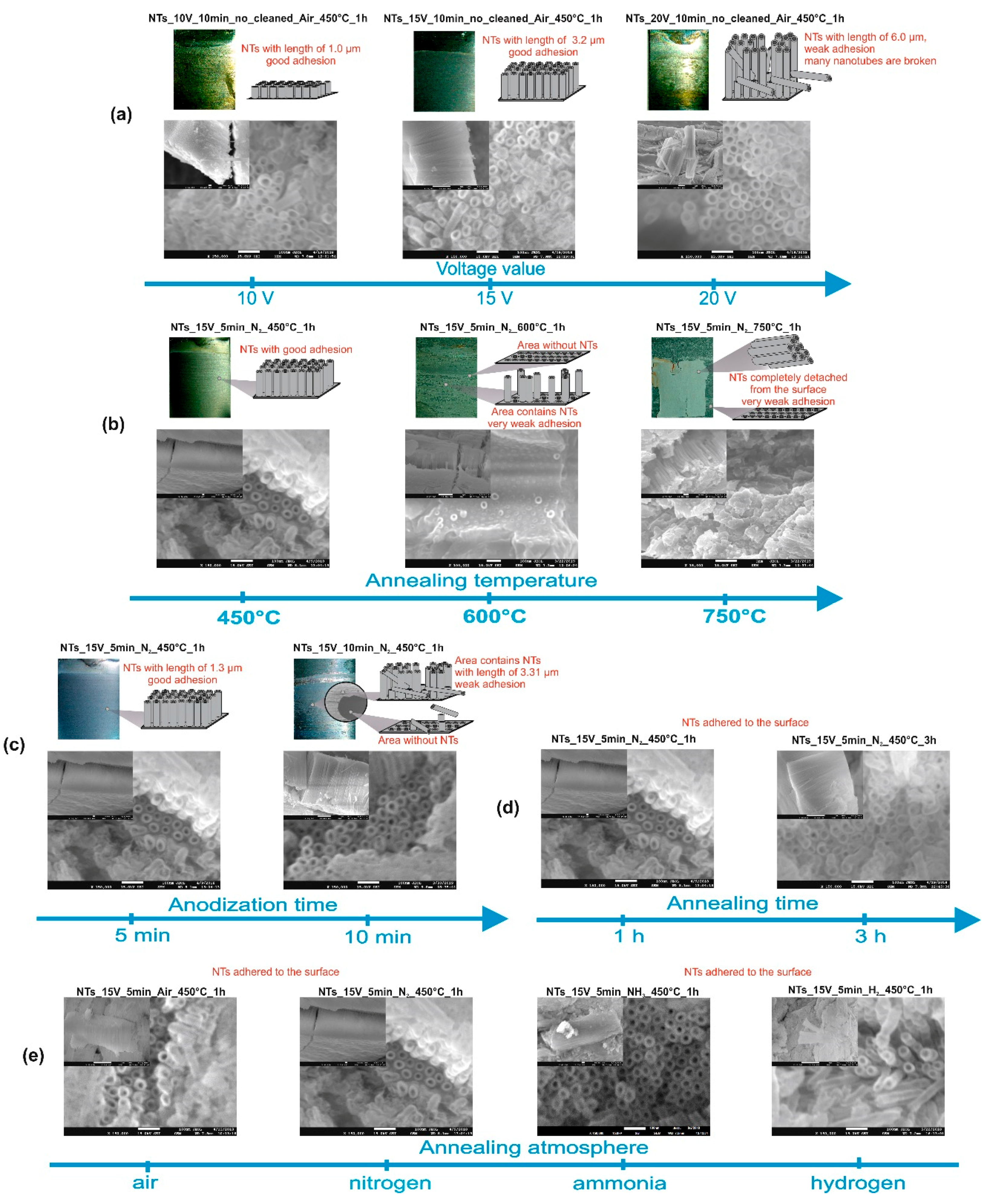
| NTs_10 V_10 min_no_cleaned_Air_450 °C_1 h | AO (U = 10 V, t = 10 min.), dried (T = 80 °C, t = 24 h), and annealed in air (T = 450 °C; t = 1 h) | 44 ± 3 | 27 ± 2 | 9 ± 1 | 1.00 ± 0.13 | High | 64.22 ± 3.27 | 90.51 ± 3.27 |
| NTs_15 V_10 min_ no_cleaned Air_450 °C_1 h | AO (U = 15 V, t = 10 min.), dried (T = 80 °C, t = 24 h), and annealed in air (T = 450 °C; t = 1 h) | 46 ± 6 | 24 ± 2 | 11 ± 2 | 3.18 ± 0.09 | High | 93.55 ± 2.38 | 97.83 ± 1.29 |
| NTs_20 V_10 min_ no_cleaned Air_450 °C_1 h | AO (U = 20 V, t = 10 min.), dried (T = 80 °C, t = 24 h), and annealed in air (T = 450 °C; t = 1 h) | 48 ± 3 | 28 ± 3 | 10 ± 1 | 6.00 ± 0.19 | Weak | 91.05 ± 3.35 | 96.82 ± 2.45 |
| NTs_10 V_10 min_N2_450 °C_1 h | AO (U = 10 V, t = 10 min.), ultrasonically cleaned (1 min.), dried (T = 80 °C, t = 24 h), and annealed in N2 (T = 450 °C; t = 1 h) | 45 ± 5 | 20 ± 3 | 11 ± 2 | 1.74 ± 0.02 | Weak | 68.38 ± 0.35 | 94.65 ± 1.91 |
| NTs_15 V_5 min_N2_450 °C_1 h | AO (U = 15 V, t = 5 min.), ultrasonically cleaned (1 min.), dried (T = 80 °C, t = 24 h), and annealed in N2 (T = 450 °C; t = 1 h) | 41 ± 4 | 19 ± 3 | 10 ± 2 | 1.27 ± 0.05 | High | 95.36 ± 1.22 | 98.73 ± 0.47 |
| NTs_15 V_5 min_N2_450 °C_3 h | AO (U = 15 V, t = 5 min.), ultrasonically cleaned (1 min.), dried (T = 80 °C, t = 24 h), and annealed in N2 (T = 450 °C; t = 3 h) | 48 ± 2 | 25 ± 4 | 10 ± 1 | 1.78 ± 0.11 | High | 91.03 ± 0.47 | 98.98 ± 0.06 |
| NTs_15 V_5 min_N2_600 °C_1 h | AO (U = 15 V, t = 5 min.), ultrasonically cleaned (1 min.), dried (T = 80 °C, t = 24 h), and annealed in N2 (T = 600 °C; t = 1 h) | 39 ± 2 | 23 ± 3 | 10 ± 2 | 1.21 ± 0.03 | Very weak | Sample was unstable | |
| NTs_15 V_5 min_N2_750 °C_1 h | AO (U = 15 V, t = 5 min.), ultrasonically cleaned (1 min.), dried (T = 80 °C, t = 24 h), and annealed in N2 (T = 750 °C; t = 1 h) | 40 ± 3 | 21 ± 2 | 10 ± 1 | 1.43 ± 0.02 | Very weak | Sample was unstable | |
| NTs_15 V_10 min_N2_450 °C_1 h | AO (U = 15 V, t = 5 min.), ultrasonically cleaned (1 min.), dried (T = 80 °C, t = 24 h), and annealed in N2 (T = 450 °C; t = 1 h) | 42 ± 3 | 21 ± 2 | 10 ± 2 | 3.31 ± 0.08 | High | 92.74 ± 1.09 | 96.81 ± 0.35 |
| NTs_15 V_5 min_Air_450 °C_1 h | AO (U = 15 V, t = 5 min.), ultrasonically cleaned (1 min.), dried (T = 80 °C, t = 24 h), and annealed in air (T = 450 °C; t = 1 h) | 49 ± 7 | 23 ± 4 | 10 ± 2 | 1.46 ± 0.20 | High | 91.86 ± 2.16 | 97.50 ± 2.40 |
| NTs_15 V_5 min_N H3_450 °C_1 h | AO (U = 15 V, t = 5 min.), ultrasonically cleaned (1 min.), dried (T = 80 °C, t = 24 h), and annealed in NH3 (T = 450 °C; t = 1 h) | 47 ± 5 | 19 ± 3 | 13 ± 1 | 2.19 ± 0.07 | High | 93.37 ± 0.42 | 98.90 ± 0.00 |
| NTs_15 V_5 min_ H2_450 °C_1 h | AO (U = 15 V, t = 5 min.), ultrasonically cleaned (1 min.), dried (T = 80 °C, t = 24 h), and annealed in H2 (T = 450 °C; t = 1 h) | 44 ± 6 | 21 ± 3 | 10 ± 1 | 1.68 ± 0.03 | High | 94.20 ± 3.43 | 98.09 ± 0.03 |
| NTs_15 V_5 min_N2_300 °C_1 h | AO (U = 15 V, t = 5 min.), ultrasonically cleaned (1 min.), dried (T = 80 °C, t = 24 h), and annealed in N2 (T = 300 °C; t = 1 h) | 47 ± 5 | 24 ± 3 | 11 ± 1 | 2.25 ± 0.06 | High | 94.08 ± 0.42 | 97.36 ± 0.25 |
| NTs_15 V_5 min_N2_450 °C_1 h_two_step | AO (I step: U = 15 V, t = 5 min.), removing of NTs layer, AO (II step, U = 15 V, t = 5 min.), ultrasonically cleaned (1 min.), dried (T = 80 °C, t = 24 h), and annealed in N2 (T = 450 °C; t = 1 h) | 46 ± 5 | 24 ± 4 | 10 ± 1 | 1.15 ± 0.05 | Weak | 89.28 ± 0.14 | 96.53 ± 0.30 |
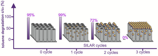
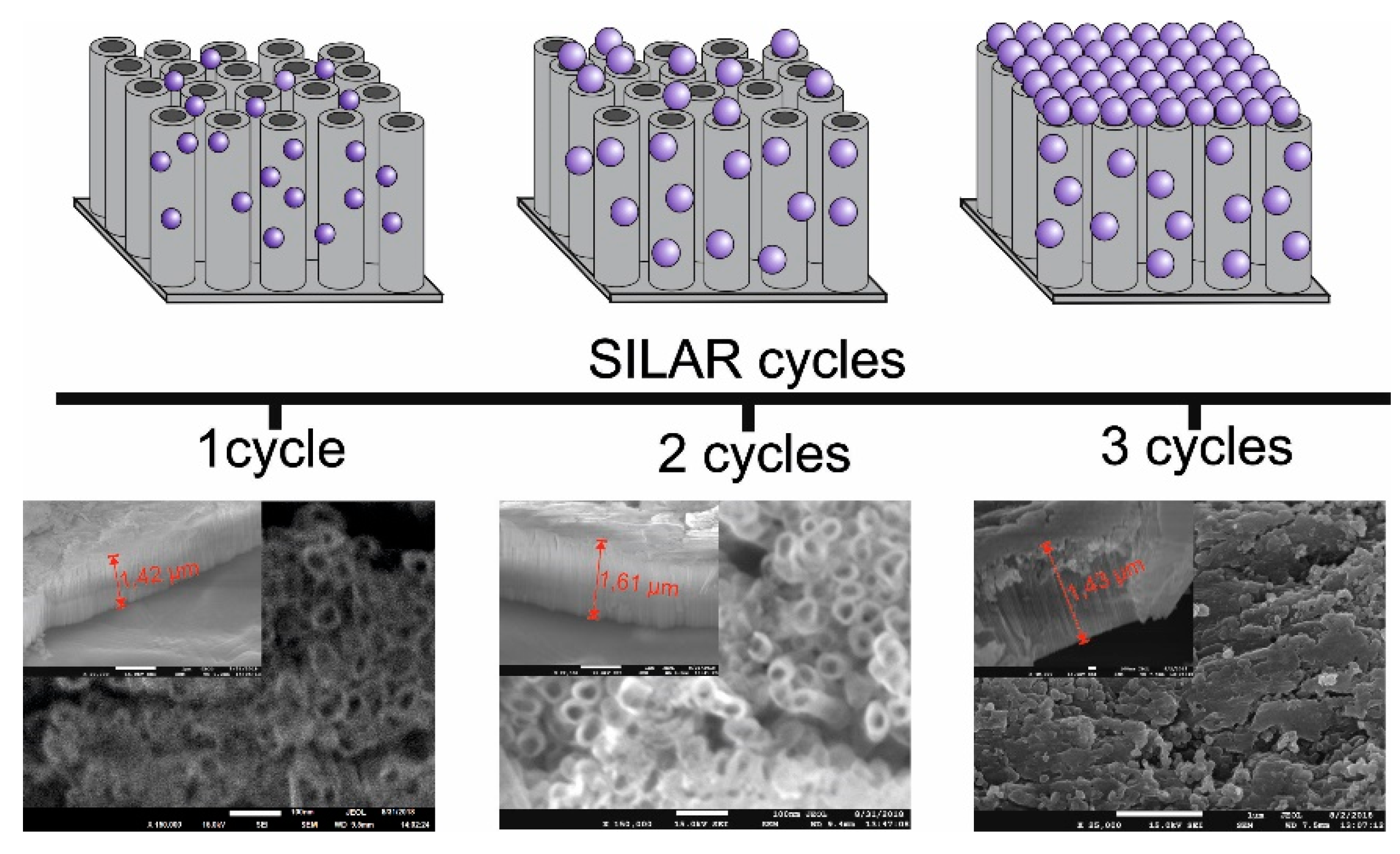
| NTs_15 V_5 min_N2_450 °C_1 h_QDs_SILAR 1x | AO (U = 15 V, t = 5 min.), ultrasonically cleaned (1 min.), dried (T = 80 °C, t = 24 h), and annealed in N2 (T = 450 °C; t = 1 h), 1 cycle of SILAR | 50 ± 4 | 31 ± 3 | 10 ± 1 | 1.42 ± 0.03 | High | 99.17 ± 0.14 | 100 |
| NTs_15 V_5 min_N2_450 °C_1 h_QDs_SILAR 2x | AO (U = 15 V, t = 5 min.), ultrasonically cleaned (1 min.), dried (T = 80 °C, t = 24 h), and annealed in N2 (T = 450 °C; t = 1 h), 2 cycles of SILAR | 41 ± 4 | 28 ± 3 | 8 ± 1 | 1.61 ± 0.11 | High | 71.56 ± 1.12 | 100 |
| NTs_15 V_5 min_N2_450 °C_1 h_QDs_SILAR 3x | AO (U = 15 V, t = 5 min.), ultrasonically cleaned (1 min.), dried (T = 80 °C, t = 24 h), and annealed in N2 (T = 450 °C; t = 1 h), 3 cycles of SILAR | Coated with Bi2S3 layer | 1.40 ± 0.05 | High | Inactive | |||
| Sample Label | Elemental Composition (at. %) | Bi 4f7/2 Fractions (%) | Ta 4f7/2 Fractions (%) | ||||||||||
|---|---|---|---|---|---|---|---|---|---|---|---|---|---|
| Ta | O | C | S | Bi | Residue (F, N, Na) | Bi0 157.0 ± 0.2 eV | Bi2S3 158.0 ± 0.3 eV | Bi2O3 159.5 ± 0.3 eV | Ta2O5_Surf 27.0 ± 0.1 eV | Ta2O5 26.2 ± 0.2 eV | Ta1+ 22.1 ± 0.1 eV | Ta0 21.0 ± 0.3 eV | |
| NTs_15 V_5 min_N2_450 °C_1 h | 22.44 | 46.00 | 24.31 | 3.10 | - | 4.15 | 0 | 0 | 0 | 0 | 96.84 | 1.72 | 1.44 |
| NTs_15 V_5 min_N2_450 °C_1 h_QDs_SILAR 1x | 15.79 | 58.20 | 11.02 | 6.26 | 2.37 | 6.36 | 2.28 | 46.50 | 51.22 | 23.55 | 73.42 | 1.86 | 1.17 |
| NTs_15 V_5 min_N2_450 °C_1 h_QDs_SILAR 2x | 16.24 | 57.47 | 12.13 | 5.66 | 2.63 | 5.87 | 3.21 | 53.10 | 43.69 | 24.81 | 72.51 | 1.91 | 0.77 |
| NTs_15 V_5 min_N2_450 °C_1 h_QDs_SILAR 3x | 0.63 | 29.47 | 26.72 | 15.14 | 22.60 | 5.44 | 1.24 | 76.58 | 22.18 | 19.61 | 80.39 | 0 | 0 |
© 2019 by the authors. Licensee MDPI, Basel, Switzerland. This article is an open access article distributed under the terms and conditions of the Creative Commons Attribution (CC BY) license (http://creativecommons.org/licenses/by/4.0/).
Share and Cite
Baluk, M.A.; Kobylański, M.P.; Lisowski, W.; Trykowski, G.; Klimczuk, T.; Mazierski, P.; Zaleska-Medynska, A. Fabrication of Durable Ordered Ta2O5 Nanotube Arrays Decorated with Bi2S3 Quantum Dots. Nanomaterials 2019, 9, 1347. https://doi.org/10.3390/nano9101347
Baluk MA, Kobylański MP, Lisowski W, Trykowski G, Klimczuk T, Mazierski P, Zaleska-Medynska A. Fabrication of Durable Ordered Ta2O5 Nanotube Arrays Decorated with Bi2S3 Quantum Dots. Nanomaterials. 2019; 9(10):1347. https://doi.org/10.3390/nano9101347
Chicago/Turabian StyleBaluk, Mateusz A., Marek P. Kobylański, Wojciech Lisowski, Grzegorz Trykowski, Tomasz Klimczuk, Paweł Mazierski, and Adriana Zaleska-Medynska. 2019. "Fabrication of Durable Ordered Ta2O5 Nanotube Arrays Decorated with Bi2S3 Quantum Dots" Nanomaterials 9, no. 10: 1347. https://doi.org/10.3390/nano9101347