Negative Differential Conductance Assisted by Optical Fields in a Single Quantum Dot with Ferromagnetic Electrodes


1
Guangdong Research Center of Photoelectric Detection Instrument Engineering Technology, and Guangdong Laboratory of Quantum Engineering and Quantum Materials, School of physics and Telecommunication Engineering, South China Normal University, Guangzhou 510006, China
2
Department of Electronic Information Engineering, Guangzhou College of Technology and Business, Foshan 528138, China
3
Guangzhou Key Laboratory for Special Fiber Photonic Devices, Laboratory of Nanophotonic Functional Materials and Devices, School of Information and Optoelectronic Science and Engineering, South China Normal University, Guangzhou 510006, China
*
Author to whom correspondence should be addressed.
Nanomaterials 2019, 9(6), 863; https://doi.org/10.3390/nano9060863
Submission received: 14 March 2019
/
Revised: 30 May 2019
/
Accepted: 4 June 2019
/
Published: 6 June 2019
(This article belongs to the Special Issue Preparation, Characterization and Utility of Quantum Dots)
Abstract
:In a single quantum dot (QD) system connected with ferromagnetic electrodes, the electron transport properties, assisted by the thermal and Fock state optical fields, are theoretically studied by the Keldysh nonequilibrium Green’s function approach. The results show that the evolution properties of the density of state and tunneling current assisted by the Fock state optical field, are quite different from those of the thermal state. The photon sideband shift decreases monotonously with the increase in the electron–photon coupling strength for the case of the thermal state, while the shift is oscillatory for the case of the Fock state. Negative differential conductance (NDC) appears obviously in a QD system contacted with parallel (P) and antiparallel (AP) magnetization alignment of the ferromagnetic electrode leads, assisted by the Fock state optical field in a wide range of electron–photon interaction parameters. Evident NDC usually only arises in an AP configuration QD system assisted by the thermal state optical field. The results have the potential to introduce a new way to actively manipulate and control the single-electron tunneling transport on a QD system by the quantum states of the optical field.
1. Introduction
Circuit quantum electrodynamics (QED) enable people to manipulate and probe with high sensitivity the quantum state of superconducting quantum bits coupled to microwave cavities. Recently, it has become possible to fabricate new devices, in which the superconducting quantum bits are replaced by hybrid mesoscopic circuits, combining nanostructure devices and metallic reservoirs. Owing to the versatility of nanofabricated circuits, the hybrid circuit QED would be suitable for a number of applications which are not accessible with standard cavity QED [1].
Because of the discrete energy spectrum and behavior similar to that of an atom [2], a quantum dot (QD)-based hybrid circuit, QED, could be used to probe the interactions of light with matter (light–matter interactions) [3,4,5,6], to implement the quantum optical device [7,8], in order to engineer new states of matter with relevance to the fields of quantum optics [9,10] and solid state physics [11,12].
The greatest advantage of the hybrid circuit QED systems is that the artificial atom properties can be arbitrarily controlled by the application of an external field. It provides a new way to study the light–matter interactions in electronic circuits. There are mainly two kinds of studies. The first class of studies focuses on the artificial atom limit, where the hybrid circuit QED can be used to manipulate and probe the electronic degrees of freedom, such as confined charges or spins. The second class of studies focuses on revealing or controlling the dynamics of electron tunneling between QD and electrode leads using a cavity photon field.
On the other hand, negative differential conductance (NDC) has attracted considerable attention due to its potential applications in the realization of low-power memory devices and logic circuits. NDC could be used to reveal the intrinsic highly nonlinear character of molecular junctions, and it appears to be related to fundamental features of electron–electron or electron–vibration interactions [13,14]. The typical system, where NDC appears, is a QD with a single orbital level, coupled to an on-site single phonon mode, and connected to leads with asymmetric tunneling rates [15]. NDC can also be found in phonon-assisted QD systems, with finite Coulomb correlation parameters, connected to an asymmetric magnetization alignment of the ferromagnetic electrode leads [16]; a double QDs system connected to symmetric or asymmetric magnetization alignment of the ferromagnetic electrodes leads [17]; and a molecular junction connected to leads with asymmetric tunneling rate [18]. In the past, the phonons, in all the phonon-assisted QD systems investigating NDC, are in a thermal state, and it is difficult to actively modulate and control the NDC. It is interesting to investigate how other quantum states influence the dynamics of electron tunneling via the interaction of a QD with another form of external field, especially the NDC property.
In this paper, the purpose is to investigate the dynamics of electron tunneling through a photon-assisted QD system connected to the ferromagnetic electrodes leads with an infinite Coulomb correlation parameter. The QD system can be implemented by the hybrid circuit QED technique, where the dynamics of electron tunneling can be controlled by the cavity photon field. The state of the assisting photon field in this paper is the Fock state, and the results are compared with that of the thermal state.
Photon-assisted electronic transport attracts great attention [19,20]. However, most of the studies employ a classical treatment for the external field, that introduces a time-dependent oscillating energy level in QD, which is valid only in the case of a high-intensity field and weak coupling [21]. It has been shown that the spectrum in the quantum case is shifted from the non-interacting spectrum, and that the shift of photon sidebands is photon-intensity-dependent [21,22]. Employing the quantum treatment of the electron–photon interaction [21] and the Keldysh non-equilibrium Green’s function approach [23,24,25,26], we study photon-assisted transport properties of electrons through a single QD connected with ferromagnetic electrode leads.
The paper is organized as follows. In Section 2, we present the physical model and theoretical calculation by the Keldysh non-equilibrium Green’s function approach, based on the quantum treatment of the optical field. In Section 3, we study the effects of the electron–photon coupling strength, bias voltage and other parameters of optical fields on the density of states and tunneling current. The conclusion will be given in Section 4.
2. Physical Model and Formalism
Figure 1 illustrates the system schematic of the QD with ferromagnetic leads coupled to a one-mode optical cavity; the QD is modeled as a one-level system. The loss of the optical field is not considered here, because we focus on the influence of the thermal and Fock state optical fields on the transport properties through a single QD.
The total Hamiltonian of the system can be written as H = HL + HR + Hph + HD + HT. The Hamiltonians for electrons in the left (L) and right (R) electrode leads are [1,8,21],
where is the conduction electron creation (annihilation) operator with wave vector k and spin σ in lead , and is the spin-dependent single-electron energy.
The third term stands for the single-mode optical field. , where is the photon creation (annihilation) operator with frequency . The electron Hamiltonian on the QD is:
where denotes the spin-dependent energy level of the QD, which can be controlled by modulating the gate voltage and λ is the coupling constant between the QD electron and photon mode, which is time-independent, and is different from the classical treatment that introduces a time-dependent oscillating energy level in QD [19,20]. The symbol e is the amount of charge on an electron, while that of is the corresponding creation (annihilation) operator of an electron in the QD, and U is the electron Coulomb correlation parameter. The last term describes the conduction electron hopping between the QD and electrode leads,
where is the spin-dependent tunneling co-efficient.
Using the Keldysh nonequilibrium Green’s function formalism, the current through the system can be obtained as [16,24,25,26],
where, fL and fR are the Fermi distribution functions for the left and right leads respectively, having different chemical potentials upon a voltage bias μL − μR = eVbias. This Vbias is the bias voltage between the two electrode leads, while is Planck’s constant. Γα ,σ represents the spin-dependent tunneling rates between QD and electrode leads, characterized by . () is the retarded (advanced) Green’s function for the QD electron coupled to the photon as well as to the leads, and is the lesser Green’s function. Equation [4] is only valid if the left and right tunneling rates are proportional to each other, i.e., , where χ is a constant [26].
It is convenient to eliminate the electron–photon coupling terms in the Hamiltonian by using a canonical transformation, i.e., with and [16,24,25]. The transformed Hamiltonian becomes , where , and
where , , , and with . can be approximated as its expectation value , which is valid only when the hopping between QD and leads is small compared to the electron-photon interaction [16,24,25]. In the new representation, the retarded Green function of the system can be written as [25]:
By the equation of motion approach [26], under the infinite-U limit, it is easy to find the Fourier transform of as [16,25,26],
where the self-energy terms are [27,28]:
where PI represents principal value integral, is the digamma function, and W is the conduction half-bandwidth of the electrode lead. is the self-energy due to the tunneling into the leads without the influence of electron-electron interaction in QD, while is the modification to the self-energy because of the electron-electron interaction in QD [26]. For convenience, we consider a constant conduction density of states for , and which is independent of wave vector k [28].
The situations for thermal and Fock state optical fields are formulated as follows.
A. If the optical field is in the thermal state . Although the results are similar to those reported in [25] of the phonon-assisted inelastic transport through a single QD with ferromagnetic electrodes for the thermal state optical field, it was mainly applied to perform a contrastive analysis for the case of the Fock state. Furthermore, the phonon-assisted spin-polarized tunneling through a QD, interacting with the thermal state phonon field under a finite Coulomb correlation parameter, has been studied in [16]. The average photon number of the thermal state is assumed to be an independently varied parameter in this paper, because the temperature of the thermal optical field can be controlled differently from the temperature of the electrode leads.
B. If the optical field is in the Fock state , using some algebra, one can obtain (see Appendix A)
where is Laguerre polynomials, is the photon number in the Fock state. Thus, the corresponding imaginary part of reads (see Appendix B)
where
and are the imaginary part and the real part of , respectively. , . . .
The averaged occupation number of the spin σ electron in a QD can be calculated by the self-consistent equations as follows [26]:
This equation is obtained from the fluctuation–dissipation theorem [26].
3. Discussion
We first discuss the influences of the thermal and Fock state optical fields on the coupling coefficient between a QD and ferromagnetic electronic leads after the canonical transformation.
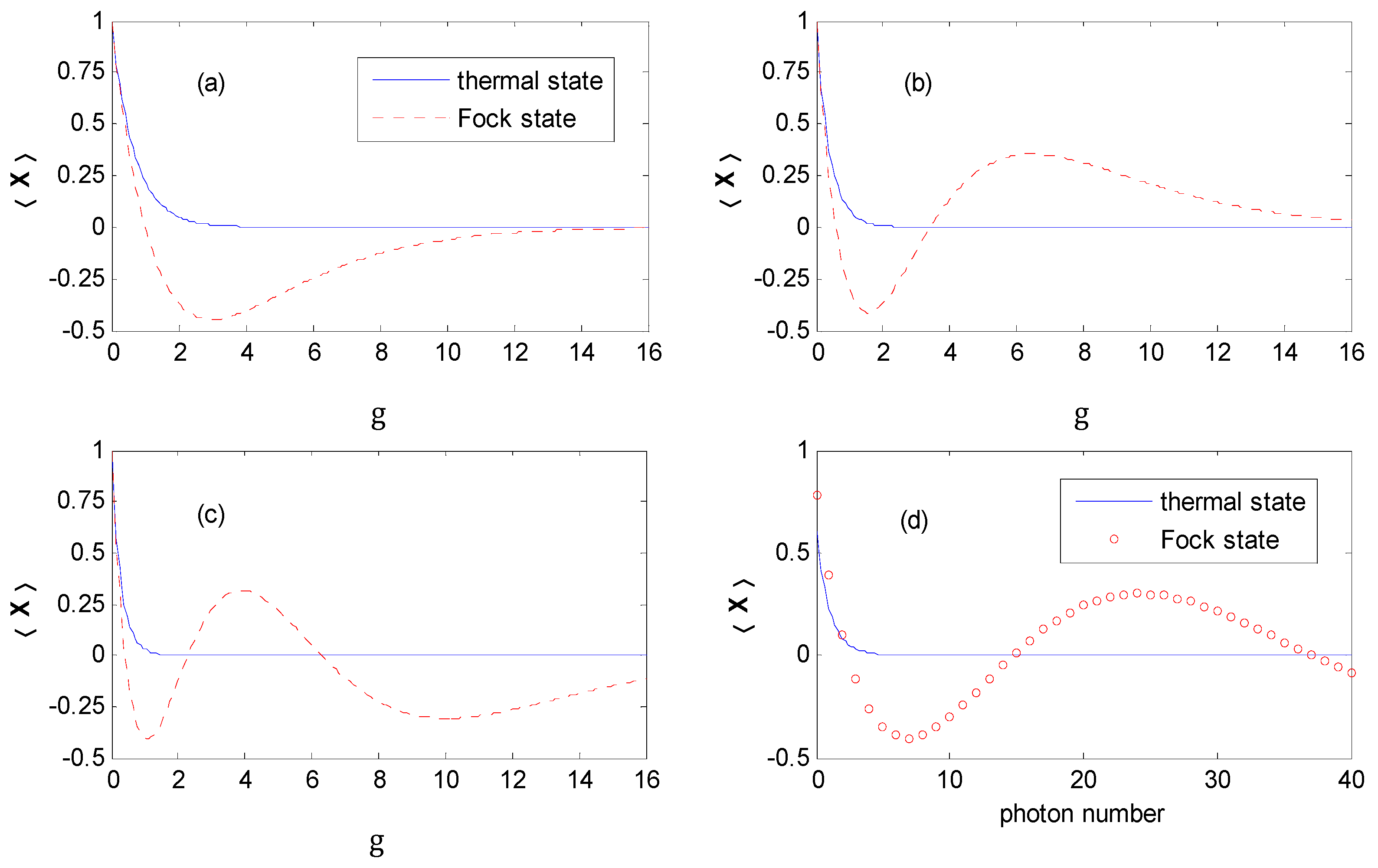
The effective QD–lead coupling coefficient may be approximated as its expectation value after the canonical transformation [24,25]. In the new representation, the electrons are dressed with a photon cloud with the interaction of QD and leads. It is easy to find for the thermal state and for the Fock state (see Appendix C).
Figure 2a shows that decreases exponentially to zero with the increase of g for the thermal state, while it reduces to a certain negative value, and then tends to zero gradually with increasing for the Fock state. Figure 2b,c show that will decrease and oscillate around the abscissa axis when approaching zero for the Fock state with an increasing photon number.
For the case of the Fock state , the curve crosses the abscissa axis times, for example, once for , twice for , and three times for and so on. The nonmonotonicity of Laguerre functions results in the oscillatory behavior. For effective coupling coefficients , the real zeros reveal that the tunneling can be critically suppressed at certain values of the g for the Fock state. We can also find that the may possess a negative value at a certain regime of g. It reveals that the Fock state optical field would change phase for when QD electron dressing with a photon cloud interacts with the electronic leads. This attests to the existence of quantum interference between transmissions through different photon sideband channels [29].
Then, we analyzed the influences of the thermal and Fock state optical fields on the effective tunneling rate of a QD and the ferromagnetic electronic leads after the canonical transformation. The expression of the effective coupling rate is . Figure 2d shows as a function of the photon number for the thermal and Fock state optical fields.
From Figure 2, we can find that the effective coupling rate is suppressed by a factor , which is determined by the parameter g and the photon number of the optical field. The real zeros appear at a certain value of g for the Fock state.
From Equation (8), Equation (9) and Equation (11), we can find that optical fields impact the shift of photon sidebands by the product factor in , and that they affect the line width of photon sidebands with the product factor in and , respectively. The amplitudes of photon sidebands are influenced by optical fields using the coefficients and in Equation (6), and in Equation (7) which is determined by the self-consistent Equation (13).
not only depends on the electron–photon coupling strength, but also on the photon intensity for the quantum state optical field. Figure 2 shows that decreases monotonously with the increase in the electron–photon coupling strength or averaged photon number for the thermal state optical field, while it becomes oscillatory upon an increasing electron–photon coupling strength or photon number for the Fock state case.
3.1. Density of State (DOS)
Here, we investigate the properties of DOS in a QD under different parameters. In the following discussions, we set with , which is the equilibrium chemical potential of the left (right) electrode lead in the absence of gate voltage . () is the chemical potential of the left (right) electrode, which is taken as . We also introduce the tunneling rate between QD and lead as and with for the P and AP magnetization alignment of the ferromagnetic electrodes, where describes the tunneling rate between the QD and lead without internal magnetization. P is the spin polarization of the ferromagnetic electrodes. , is the temperature of the electrode leads. For simplicity, we state that the energy unit is taken as the photon energy , and the unit of is . W is set as in this article.
Moreover, when the temperature of the electrode lead approaches the Kondo temperature , the decoupling approximation, used in the derivation of Equation (7), could lead to some drawbacks due to the logarithmic divergence of the digamma function. Specifically, the divergence of the digamma function could lead to incorrect behavior of the DOS at the Fermi level [30]. Thus, in this paper, we assume that the temperature of the electrode lead is higher than the Kondo temperature determined by the method in [31].
Up to now, as far as we know, there is no experiment on NDC based on a photon-assisted QD system. However, there exist several experiments on NDC based on a phonon-assisted carbon tube system [32,33]. The NDC features can be described quite simply using a generic model which consists of a quantum dot with a single-orbital level, coupled to an on-site single phonon mode, and connected to leads by tunnel junctions [15]. Thus, we set the numeric values of the parameters in this paper with reference to that in [15,24,25,32,33]. We also set the photon energy as an elementary scale, and give the units of other parameters with and the amount of charge on an electron e.
Here, we begin to discuss DOS for the system under different parameters.
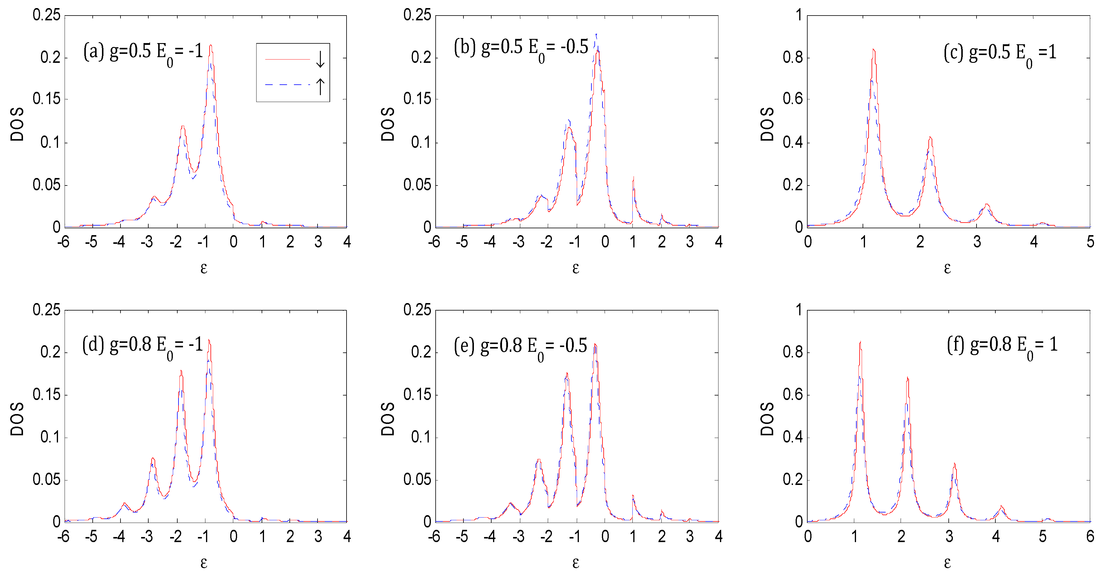
Because the thermal state and Fock state become the vacuum state when the photon number equals to zero, Figure 3 shows the DOS changes with E0 and g for the vacuum state. One can find that the main peaks appear near the location at , which are the channels for electron transport without any participation of a photon. Figure 3b,e show that both sides of the main peak appear as a series of satellite peaks. The electron–photon interaction has at least two effects: It results in an energy shift of the elastic peak position relative to that for g = 0, and leads to a set of new peaks induced by photon emission. The nth sideband peak on the right (left) side with respect to the main peak near the location at E0 corresponds to the nth photon emission sideband of the electron (hole) transport. The electron (hole) contribution comes from the first (second) term on the right-hand side of Equation (11), respectively [16,24,25].
Compared with that of E0 = −1, the main peak and sideband width are compressed, the peaks of sidebands become larger and evidently shift to the right with the increase in E0, as shown in Figure 3a–f. The weight of photon sidebands transfers gradually from the left to the right of the main peak, and the line shape of each photon satellite shows a jump discontinuity [34] with respect to ω in Figure 3b,e [24]. This is because when the effective QD electron energy level approaches to Fermi surface, the electrons (holes) near the Fermi surface dominate the tunneling process, and the sharp change of Fermi functions near the Fermi surface level at the lower temperature results in the jump discontinuity. This behavior is consistent with that obtained for electron–phonon coupling in [16,24,25]. An increasing number of photon sidebands appear with increasing g, and all peak values of the sidebands increase as g becomes greater, even in the vacuum state of the optical field, which is quite different from those of the case under classical treatment for the external field [20]. The width of main peak is compressed as the increase of g.
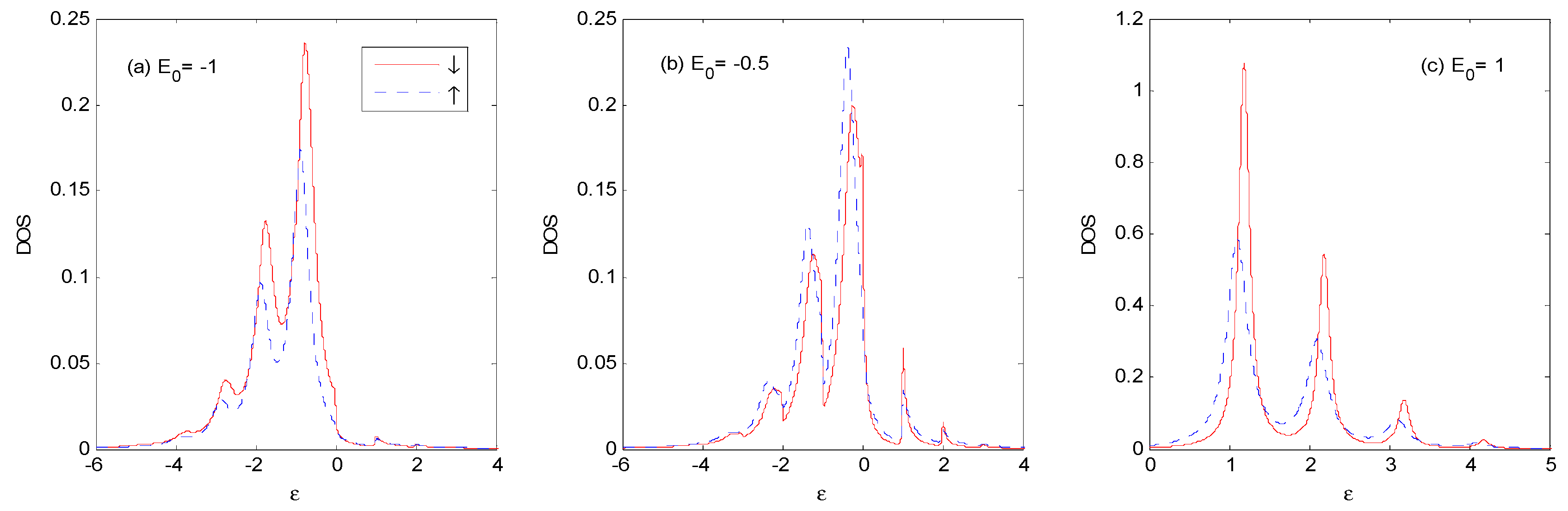
Comparing Figure 4a–c with Figure 3a–c respectively, although the difference between spin up DOS and spin down DOS is larger as P = 0.31 [25] and the higher spin polarization could result in a higher spin-dependent splitting in DOS, the envelopes of DOS are similar to each other respectively. Without loss of generality, we set P = 0.1 throughout this paper.
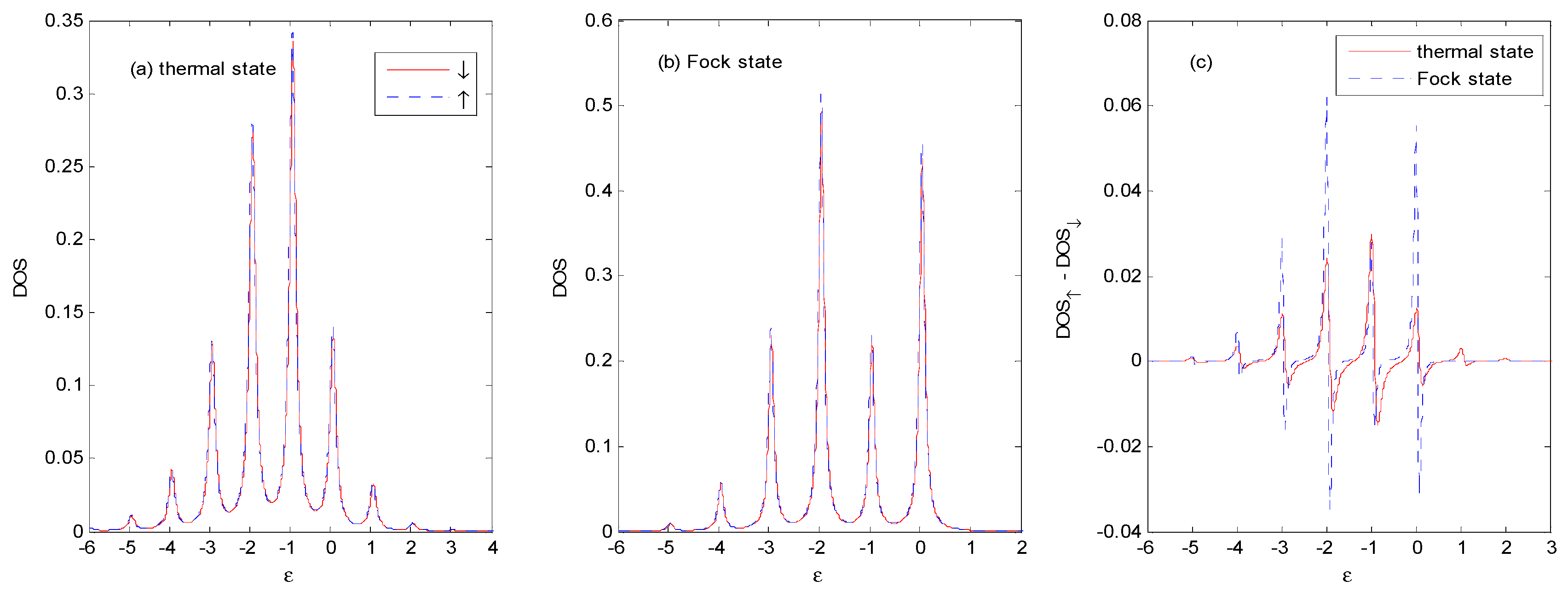
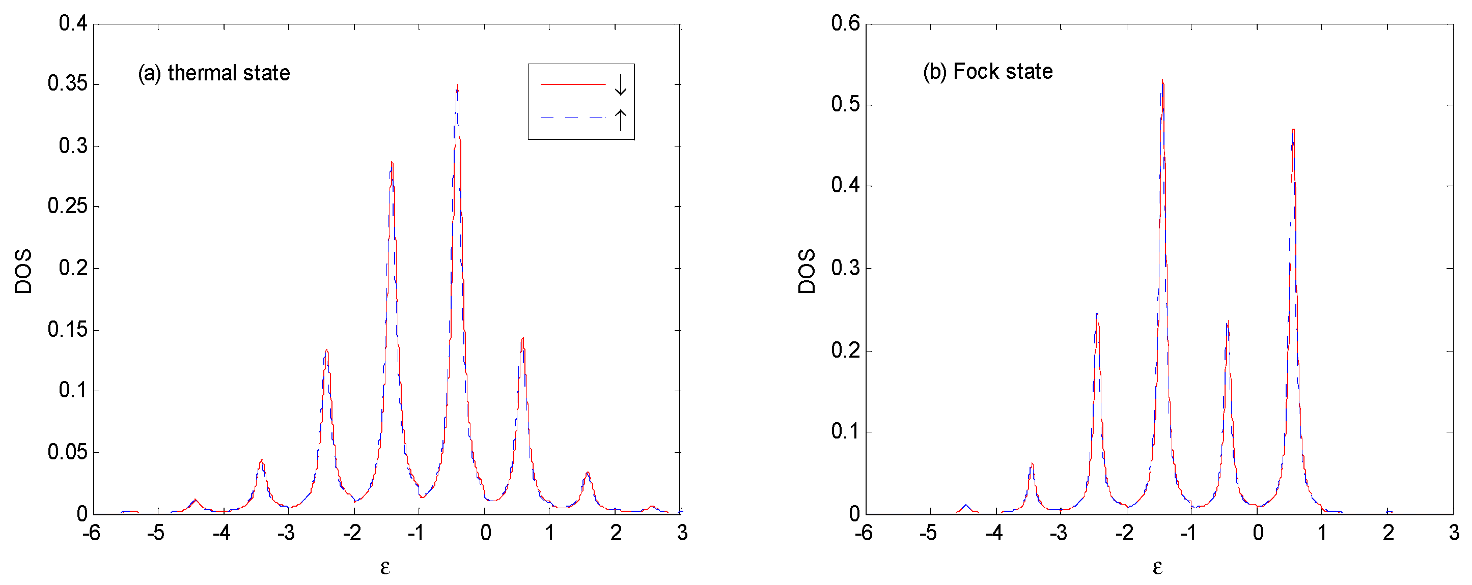
Figure 5 shows the different stages of evolution of the DOS with the thermal and Fock state optical fields for E0 = −1 and Nth = NFock = 1. Compared with Figure 3a, when the photon intensity is non-zero, the weight of main peak near becomes larger, accompanied with compressed width, and photon satellites are evident on both sides of the main peak. Photon satellites exist above the Fermi surface, while they are almost non-existent for the vacuum state in Figure 3a, as it can only absorb photons from the external optical field.
As there is definitely one photon in the Fock state (while the one-photon probability is only 25%, and the zero-photon probability is 50% in the thermal state, with an average photon number of Nth = 1), the photon sideband peaks for the case of the Fock state are higher, and the weight of the main peak is lower than those of the thermal state. There are photon satellites above the Fermi surface for the case of the thermal state because of the non-vanishing multi-photon probabilities.
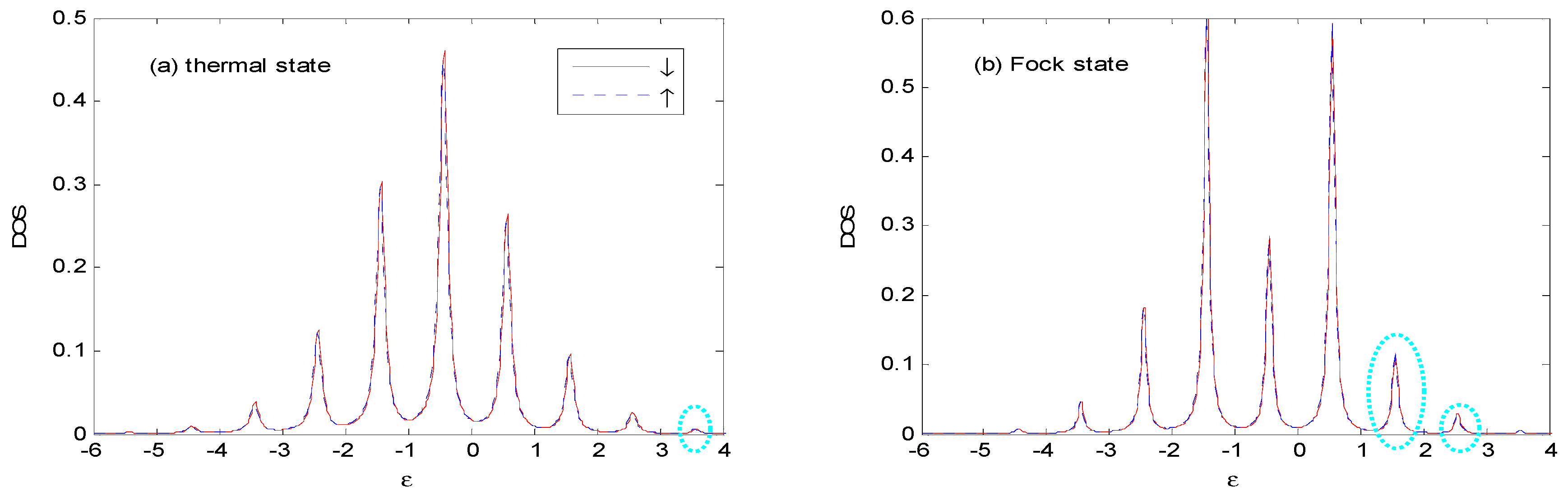
Figure 5c shows that the DOS is spin-dependent because of the spin polarization of the ferromagnetic electrodes [25]. There is a small spin splitting of the sideband in the P configuration, which comes from the spin-dependent real part of the self-energy in Equation (9). The spin splitting of DOS increases with the increasing value of the spin polarization parameter P of the ferromagnetic electrodes.
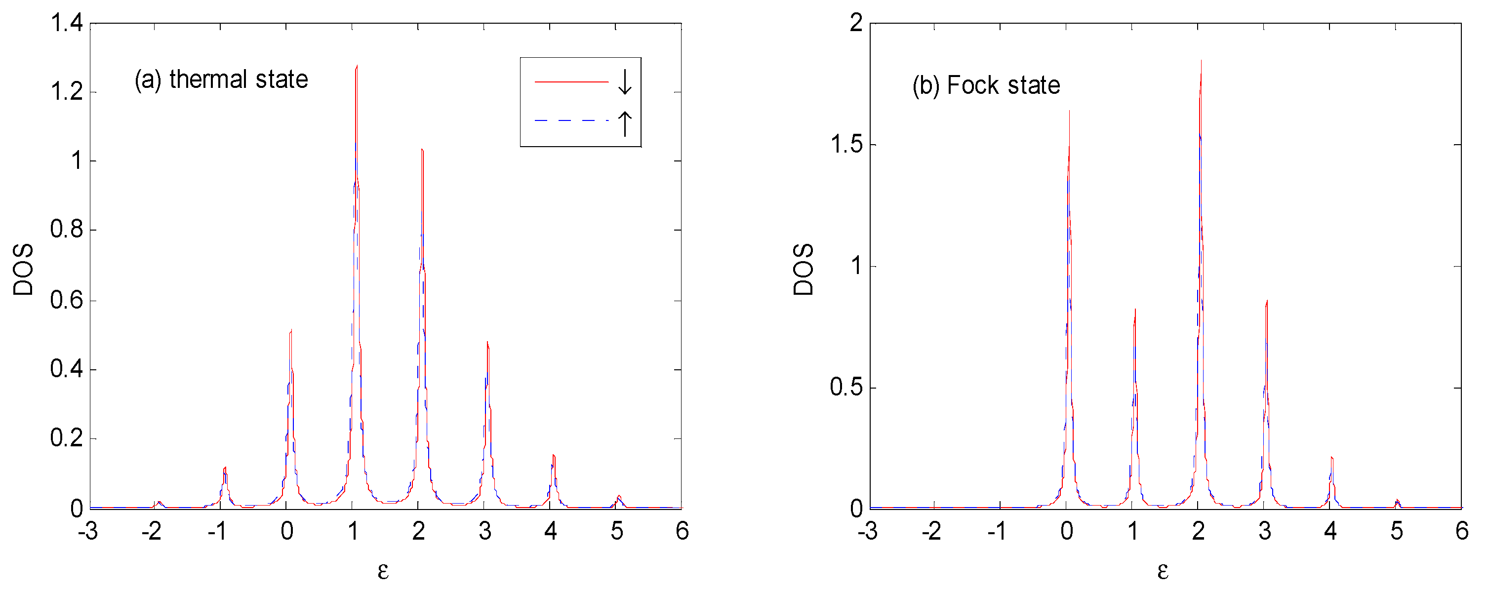
When E0 changes to −0.5 in Figure 6, the DOS is obviously changed in the thermal and Fock state optical fields. The weight and width of main peak is almost the same as that in Figure 5. The weight of the photon sidebands transfers gradually from the left to the right of the main peak, such as those in Figure 5. There are photon satellites above ε = 1 for the thermal state because the multi-photon probabilities are non-vanishing.
From Figure 5 to Figure 7, one can find that the DOS noticeably changed with the increasing of E0 in the thermal and Fock state optical fields. The weight of main peak near becomes larger accompanied by a compressed width for thermal state, and the weight of main peak becomes smaller, accompanied by a compressed width for Fock state. Almost all of the photon satellites are transferred to the right side of the main peak for the Fock state because pure electron transport predominantly contributes to the DOS [25]. There are photon-satellites that exist below the Fermi surface for the thermal state because the multi-photon probabilities are non-vanishing, while this is not the case for the Fock state optical field.
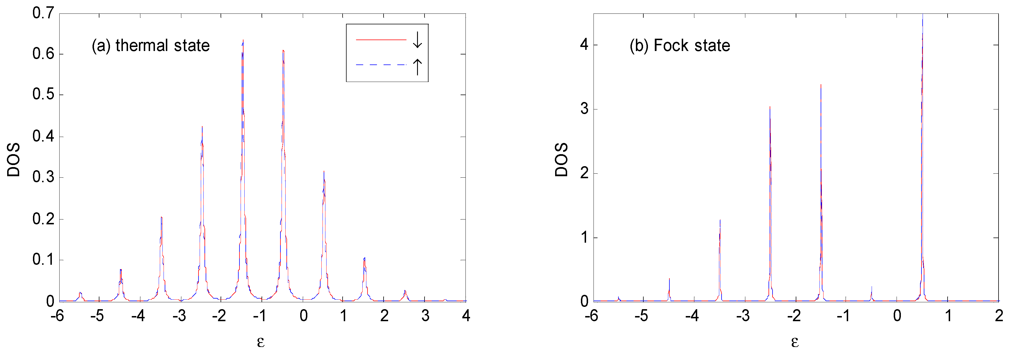
Comparing Figure 8 with Figure 6, we find that the DOS for different states evidently varies with the parameter, g. With the increase of the electron–photon coupling parameter, g, the height of the main peak decreases, while the heights of the photon-assisted sideband peaks increase, which indicates a higher probability of photon–emission or photon absorption. The widths of these peaks become narrower since, according to the discussions of Figure 2, the system is trapped in a region of exponentially-suppressed tunneling rates with increasing values of the g parameter [16]. We can also find that the pedestals of each sideband overlap for smaller electron–photon coupling parameters, g, while they tend to have well-defined boundaries at larger electron–photon coupling parameters, g. With the increase of g, an increasing number of photon sidebands appear, and the peak value increases.
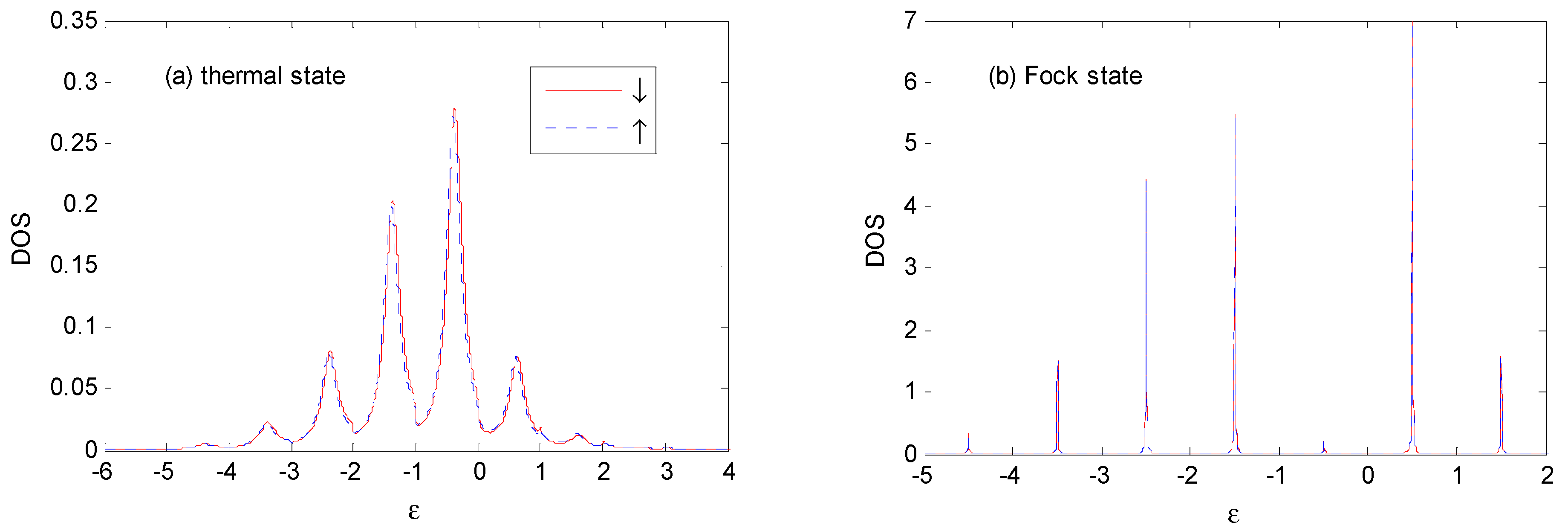
By the comparison of Figure 9 with Figure 3b, Figure 3e and Figure 6, it could be found that the amplitudes of the main peak and photon satellites increase with increasing photon intensity. Comparing Figure 9b with Figure 6b, one can find that the weight of the main peak near is almost equal to zero and a new sideband appears at when the photon number of the Fock state equals 2. The reason is that the source lead electron (hole) at the Fermi surface can absorb (emit) 2 photons to get to and form a new sideband. It is evident that the weights of photon satellites increase, while the peak widths become narrower, when the photon number increases from 1 to 2. The reason for this is that the suppression factor of the tunneling rate is enhanced as the photon number increases, which is discussed in Figure 2.
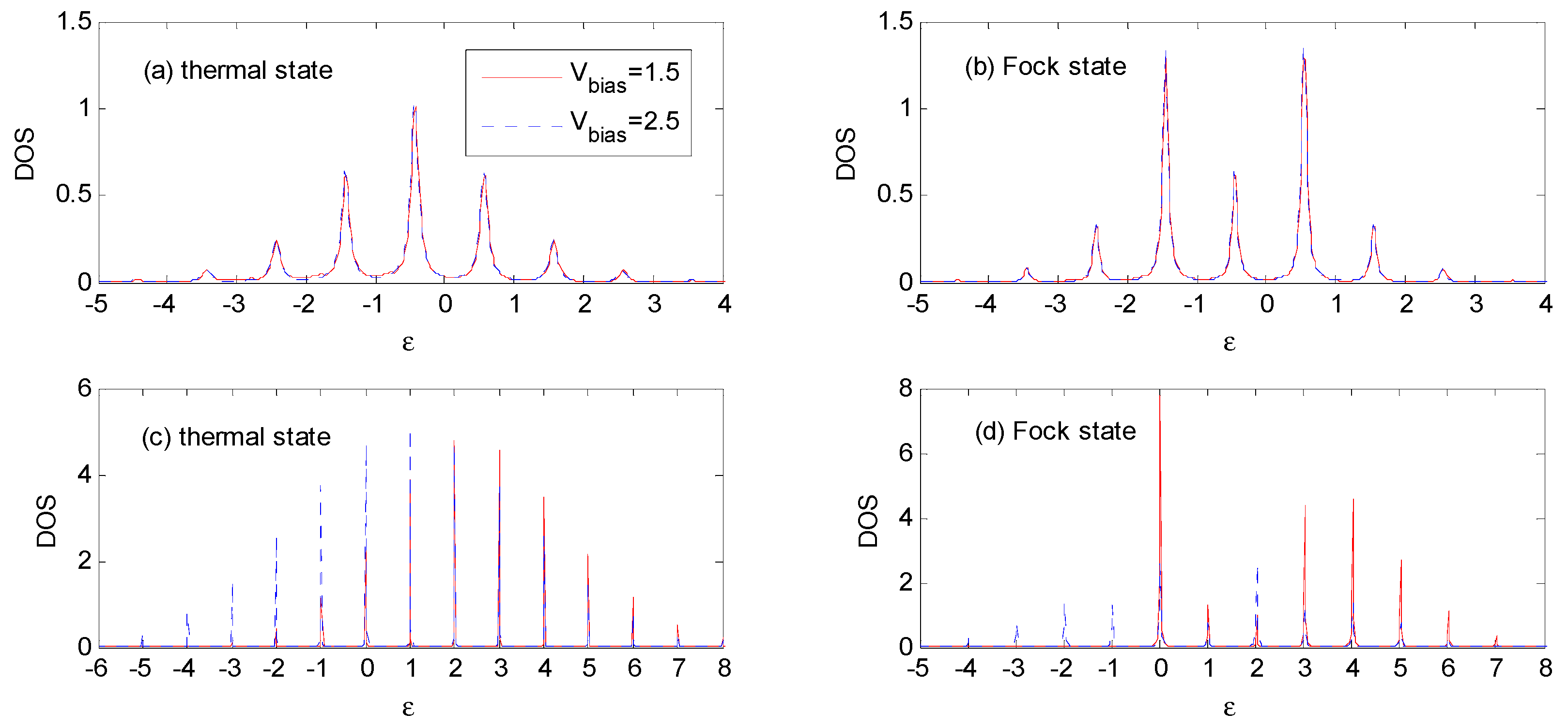
Total DOS (the sum of spin up and down DOS) are shown in Figure 10 at different bias voltage in the thermal and Fock state optical fields with different effective QD energy levels and different electron–photon coupling constants. It can be seen that there are slight differences in the total DOS for different bias voltages at E0 = −0.5 and g = 0.5; however, the height and location of the sideband is quite different for diverse bias voltage at E0 = 1 and g = 1.5. There are new sidebands that appear at for Vbias = 2.5 (blue line) with respect to Vbias = 1.5 (red line) in Figure 10c, and new sidebands appear at for Vbias = 2.5 with respect to Vbias = 1.5 in Figure 10d. The weights of the sidebands that appear at for Vbias = 2.5 are different from that for Vbias = 1.5 in Figure 10c respectively, and the weights of sidebands appearing at for Vbias = 2.5 are quite different from that for Vbias = 1.5 in Figure 10d respectively. This can lead to complex current–voltage characteristics in the thermal and Fock states, which are discussed in the next section.
Figure 11 demonstrates DOS at different leads’ temperatures for the thermal and Fock state optical fields. An increasing number of photon emission (absorption) sidebands appear (within circle) with the increase of leads’ temperature, and the peak value of the sideband increases with the increasing of leads’ temperature because this results in an increasing number of leads’ electrons above the Fermi surface. With the increasing of leads’ temperature, the weight of main peak becomes larger, accompanied with compressed width for both thermal state and Fock state compared with Figure 6.
Comparing Figure 12 with Figure 6, it can be seen that the properties of the DOS, for the antiparallel (AP) configuration are similar to those in parallel (P) configuration, and there is no difference in DOS between the spin-down and spin-up orientations at zero bias voltage. Thus, it is not necessary to discuss these further for the AP configuration.
3.2. Current
From the discussions above, we find that the DOS is sensitive to the QD energy level, electron–photon interaction and bias voltage at the leads, and the evolution characteristics of DOS for the cases of external optical fields in the thermal and Fock states are quite different. Thus, in this section, we will investigate the properties of the tunneling current–voltage characteristics upon changing the QD energy level, and the electron–photon interaction for the cases of external optical fields in the thermal and Fock states.
Because the mismatch of spin-dependent Fermi wave vectors for the AP configuration can result in a decrease of the transmission probability of electrons or holes, the current for the P magnetization alignment is significantly larger than that for the AP configuration [25]. Therefore, we mainly discuss the tunneling current for the P configuration here. In the following discussion, we denote as , as I, and the differential conductance , respectively.
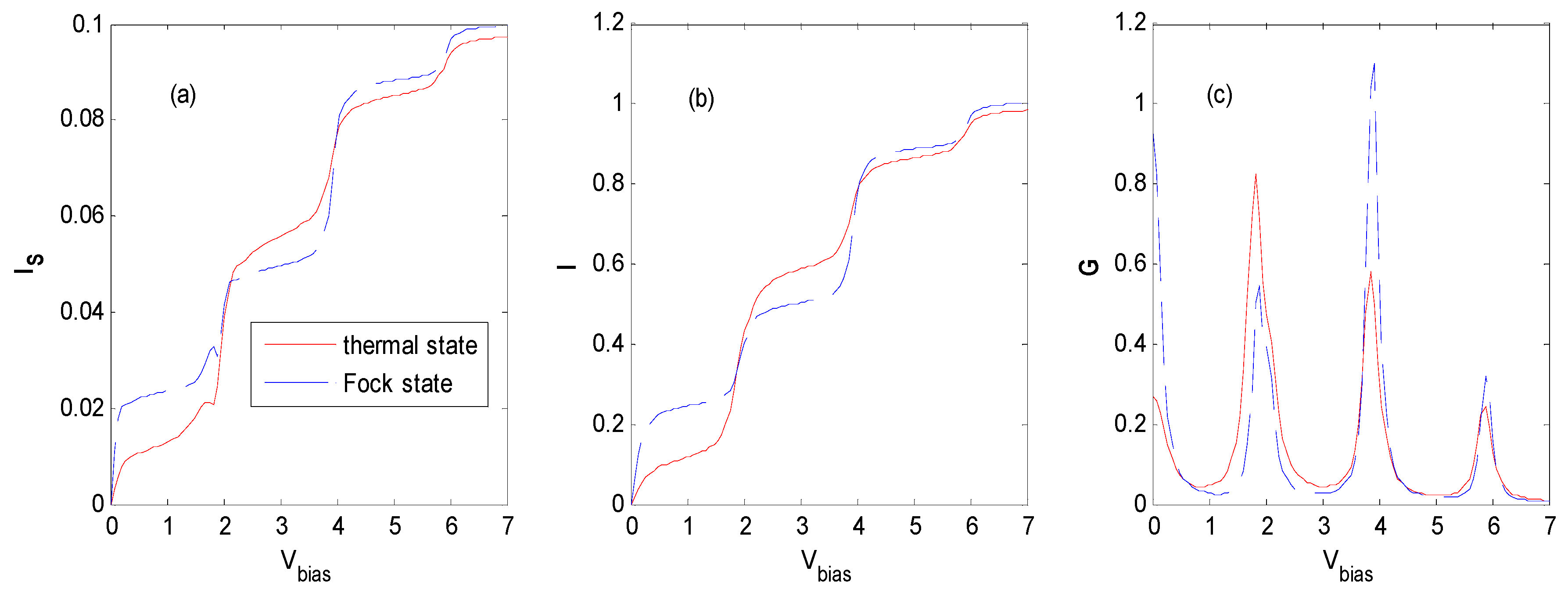
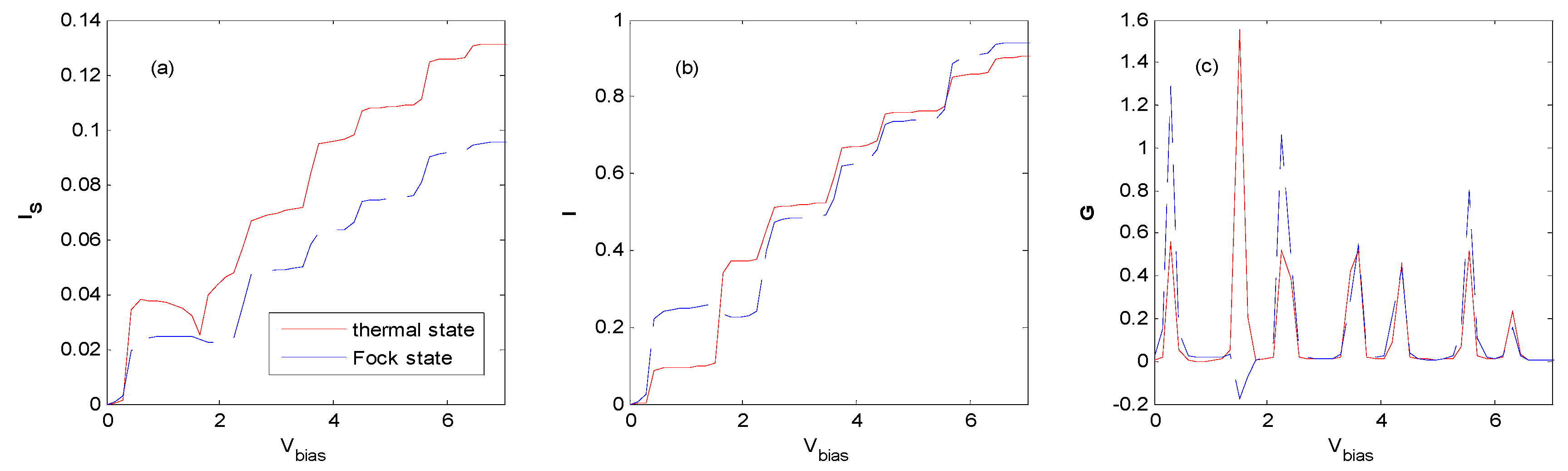
Figure 13 demonstrates the well-known staircase shape current for the different states of optical fields [16,20,24,25]. Because the QD electron has a non-vanishing probability of occupying the photon sidebands, once photon sidebands enter the bias window one by one, the photon-assisted channel would open. Thus, the tunneling processes may be mediated by the photon energy levels, which results in additional steps in the current. It shows that the currents for the cases of the thermal and Fock states tend to have a similar value of saturation at a higher bias voltage, while the currents evolve differently at lower bias voltage. From Figure 13, it can be found that the currents tend to reach their saturation value in four steps in the thermal and Fock states upon increasing the bias voltage, even when there is a little difference in the current–voltage characteristics between them. The different tunneling properties of a QD electron dressed with different-state photons result in a different shape of the current curve.
Figure 13a also demonstrates that there is a small fluctuation of spin current at each step because of the tiny difference of spin DOS discussed in Figure 5c.
By comparison of Figure 13c and Figure 5, it can be found that differential conductance reflects the DOS properties of a QD system. As the increase of bias voltage, the differential conductance peaks appear only when the lead chemical potential is aligned with the peaks of the DOS. In the vicinity of the zero bias voltage regions, where the sequential tunneling current is exponentially suppressed, the differential conductance is due to higher-order tunneling processes. The amplitude of each differential conductance peak reveals the amplitude of the main peak and photon sideband of the DOS of a QD system.
As the effective energy level E0 changes to −0.5 and 1, respectively, they have similar current–voltage characteristics for spin current and total current in Figure 13, except that the fluctuation of the spin current at each step becomes larger as the effective energy level E0 changes from −1 to −0.5 and 1, respectively.
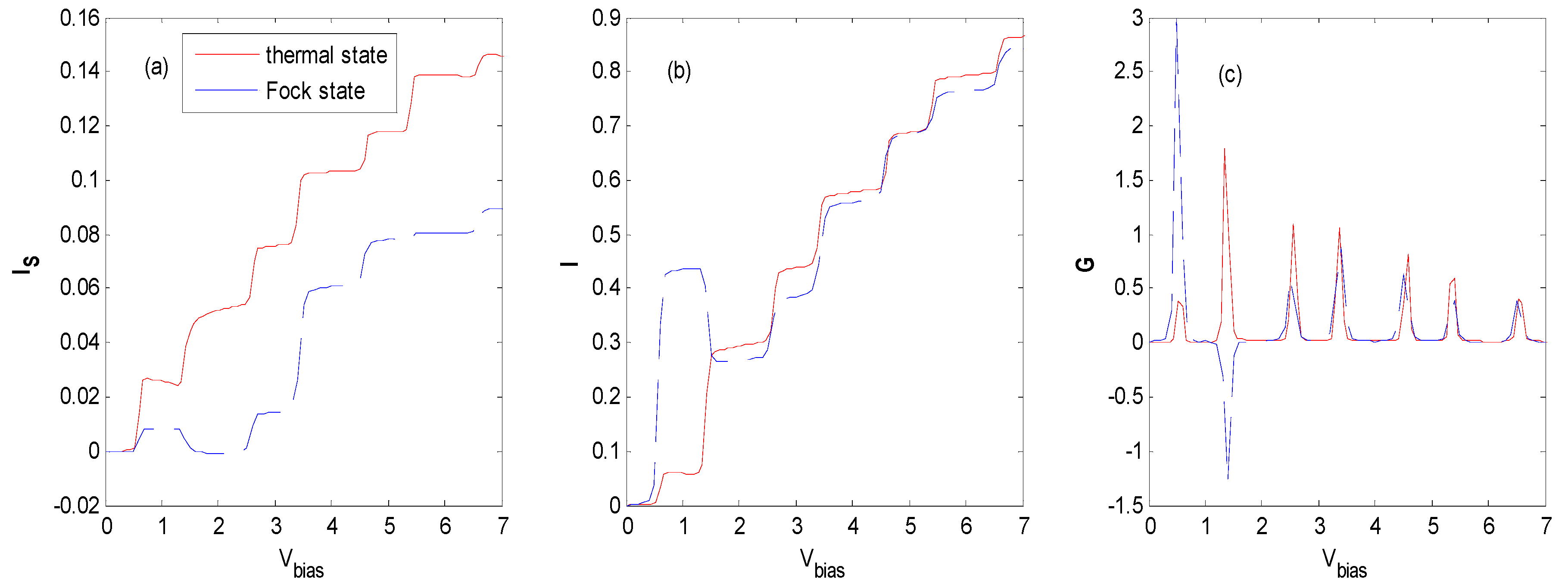
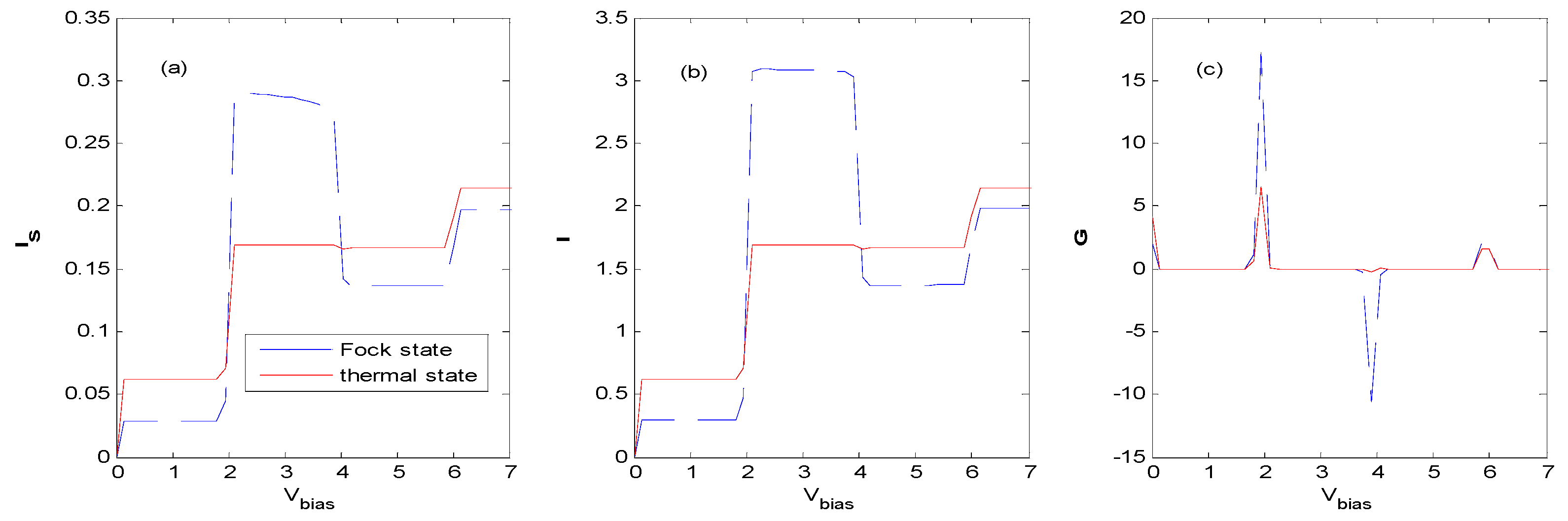
There are two types of competing mechanisms. One is that a stronger electron–photon interaction can enhance the photon emission (absorption), through which the photon-assisted tunneling channel forms, which is favorable to the formation of photon satellites. The other is an exponential suppression of the effective coupling between the QD and leads. This competition may result in NDC in the photon-assisted spin-polarized tunneling through an interacting QD with antiparallel configuration (AP) under a finite Coulomb correlation parameter [16]. From the discussions of Figure 2, one can find that the tunneling rates between the QD and leads can approach zero in some regions of the electron–photon interaction, which means the tunneling through QD is critically suppressed. Thus, we could investigate NDC in the vicinity of zero regions in Figure 2 and Figure 14, Figure 15 and Figure 16 confirms this assumption.
With the proper effective QD energy level, Figure 14, Figure 15 and Figure 16 show that there are NDCs for a QD system interacting with an external field of the Fock state at the vicinity of the first zero as the photon number is 1 (Figure 14), at the vicinity of the first zero (Figure 15) and the second zero (Figure 16) as the photon number is 3, respectively. NDC also appears in a similar parameter region as when the photon number is 2, or with the AP configuration (not shown). Figure 16 shows that a subtle NDC also exists for the case of the thermal state with the same parameter. This can be deduced from Figure 10, where the height and the location of the photon sideband peaks change as the bias voltage changes, indicating the change in the probability of photon-emission or photon-absorption. If the height of the photon sideband or the number of photon sidebands inside the bias voltage window decreases with the increasing bias voltage, NDC appears. The physical process can also be described as follows [16]. When electrons tunnel through the QD from the left electrode to the right one in the vicinity of the zero bias voltage regions, higher-order tunneling processes exist, while the sequential tunneling is exponentially suppressed. If the Vbias is sufficiently large, the photon sideband enters the bias voltage window, and photon-assisted tunneling current starts to flow through the QD. Subsequently, the tunneling current plateau is observed. Above the current plateau, an NDC is observed because the tunneling current is suppressed by an electron residing on the QD. Finally, when the next photon sideband crosses the Fermi level of the source lead, the current increases again and shows a tendency towards saturation.
The Hamiltonian model discussed in this paper is similar to that of a single molecular junction in [16], except that the state of the external field is the Fock state in this paper. However, we find that obvious NDC appears in a single QD system assisted by the Fock state optical field with both P and AP configurations, while evident NDC only emerges in an AP configuration in [16]. In this paper, NDC can be obtained for a wide range of electron–photon interaction parameters at the vicinity of the zeros of the Laguerre function (see Figure 2), because there is an increasing number of zeros when the photon number of the Fock state increases.
4. Conclusions
Based on the effect of quantum treatment on an optical field, we have investigated the quantum transport through the single QD with ferromagnetic electrodes in the presence of an electron–photon interaction by the Keldysh nonequilibrium Green’s function approach. The important results can be briefly summarized as follows.
Firstly, owing to the interaction with optical fields, the shift of photon sidebands is dependent on the electron–photon coupling strength and the photon intensity. For an increasing electron–photon coupling strength, the shift is monotonically decreasing for the case of the thermal state optical field, while it is oscillatory for the Fock state optical field because of the nonmonotonicity of Laguerre functions.
Secondly, the DOS and the tunneling current are sensitive to the QD energy level adjusted by the gate voltage and the electron–photon interaction. The evolution properties of DOS and tunneling current for photon-assisted spin-polarized tunneling with the Fock state of optical field, are quite different from that with the thermal state case.
Thirdly, obvious NDC can be found in both P and AP configuration QD systems assisted by the Fock state optical field in a wide range of electron–photon interaction parameters, while evident NDC usually only arises in an AP configuration QD system assisted by the thermal state optical field.
These important results enlighten us that a single-electron tunneling transport in a QD can be actively manipulated and controlled by quantum states of the optical field. Meanwhile, the information of the spectral function of QD and the interaction with external optical fields could be inferred from the spectra of the tunneling current. Furthermore, NDC has potential applications in the realization of low-power memory devices and logic circuits. Thus, the results would deepen the understanding of single-electron tunneling transport properties in QD, enrich the control techniques for the transport of QD electrons, and open a new door for constructing nanostructured devices and spin-dependent devices.
Author Contributions
All Authors prepared the manuscript and contributed to the concepts and theoretical results exposed in this article. Numerical calculations were run by W.L. All authors have read and approved the final manuscript.
Funding
This work was funded by National Natural Science Foundation of China ((Grant Nos. 61575067, 61774062 and 61275059)), Foundation for Distinguished Young Talents in Higher Education of Guangdong, China (Grant No. 2016KQNCX195), and the Research Fund Program of Guangdong Provincial Key Laboratory of Nanophotonic Functional Materials and Devices.
Conflicts of Interest
The authors declare no conflict of interest.
Appendix A. The Derivation of Equation (10) and Equation (12)
Using the same method of the appendix A of [35], one can obtain:
where , is Laguerre Polynomial. Thus, the correlation function can be rewritten as:
Here, . In the last step, we have used the following equation [36]:
Finally, the correlation function can be rewritten in following form:
where .
Appendix B. The Derivation of Equation (11)
Based on the Equation (A3), Equation (6) can be rewritten as:
After the Fourier transform, one obtains:
By the method of the equation of motion [26], under the limitation of , one can obtain:
Appendix C. The Derivation of
Using the Baker-Campbell-Haussdorf relation, one can obtain:
And using the Equation (A1), we find:
which is for the Fock state.
Here, we have used the generating function in the last step, and .
References
- Cottet, A.; Kontos, T.; Douçot, B. Electron-photon coupling in mesoscopic quantum electrodynamics. Phys. Rev. B 2015, 91, 205417. [Google Scholar] [CrossRef]
- Kouwenhoven, L.; Marcus, C. Quantum dots. Phys. World 1998, 11, 35. [Google Scholar] [CrossRef]
- Cohen-Tannoudji, C.; Dupont-Roc, J.; Grynberg, G. Atom-Photon Interactions: Basic Processes and Applications; Wiley-VCH: Weinheim, Germany, 1998. [Google Scholar]
- Powell, R.C. Physics of Solid-State Laser Materials, Atomic, Molecular and Optical Physics Series; Springer: New York, NY, USA, 1998. [Google Scholar]
- Delbecq, M.R.; Schmitt, V.; Parmentier, F.D.; Roch, N.; Viennot, J.J.; Fève, G.; Huard, B.; Mora, C.; Cottet, A.; Kontos, T. Coupling a quantum dot, fermionic leads, and a microwave cavity on a chip. Phys. Rev. Lett. 2011, 107, 256804. [Google Scholar] [CrossRef] [PubMed]
- Hartke, T.R.; Liu, Y.Y.; Gullans, M.J.; Petta, J.R. Microwave detection of electron-phonon interactions in a cavity-coupled double quantum dot. Phys. Rev. Lett. 2018, 120, 097701. [Google Scholar] [CrossRef] [PubMed]
- Agarwalla, B.K.; Kulkarni, M.; Mukamel, S.; Segal, D. Giant photon gain in large-scale quantum dot-circuit QED systems. Phys. Rev. B 2016, 94, 121305. [Google Scholar] [CrossRef] [Green Version]
- Kulkarni, M.; Cotlet, O.; Türeci, H.E. Cavity-coupled double-quantum dot at finite bias: Analogy with lasers and beyond. Phys. Rev. B 2014, 90, 125402. [Google Scholar] [CrossRef] [Green Version]
- Goban, A.; Hung, C.L.; Hood, J.D.; Yu, S.P.; Muniz, J.A.; Painter, O.; Kimble, H.J. Superradiance for atoms trapped along a photonic crystal waveguide. Phys. Rev. Lett. 2015, 115, 063601. [Google Scholar] [CrossRef] [PubMed]
- Sipahigil, A.; Evans, R.E.; Sukachev, D.D.; Burek, M.J.; Borregaard, J.; Bhaskar, M.K.; Nguyen, C.T.; Pacheco, J.L.; Atikian, H.A.; Meuwly, C.; et al. An integrated diamond nanophotonics platform for quantum optical networks. Science 2016, 354, 847–850. [Google Scholar] [CrossRef]
- Smolka, S.; Wuester, W.; Haupt, F.; Faelt, S.; Wegscheider, W.; Imamoglu, A. Cavity quantum electrodynamics with many-body states of a two-dimensional electron gas. Science 2014, 346, 332–335. [Google Scholar] [CrossRef]
- Tredicucci, A.; Chen, Y.; Pellegrini, V.; Börger, M.; Sorba, L.; Beltram, F.; Bassani, F. Controlled exciton-photon interaction in semiconductor bulk microcavities. Phys. Rev. Lett. 1995, 75, 3906–3909. [Google Scholar] [CrossRef]
- Sapmaz, S.; Jarillo-Herrero, P.; Blanter, Y.M.; Zant, H.S.J.V.D. Coupling between electronic transport and longitudinal phonons in suspended nanotubes. New J. Phys. 2005, 7, 243. [Google Scholar] [CrossRef]
- Xu, B.; Dubi, Y. Negative differential conductance in molecular junctions: An overview of experiment and theory. J. Phys. Condens. Matter 2015, 27, 263202. [Google Scholar] [CrossRef] [PubMed]
- Zazunov, A.; Feinberg, D.; Martin, T. Phonon-mediated negative differential conductance in molecular quantum dots. Phys. Rev. B 2006, 73, 115405. [Google Scholar] [CrossRef] [Green Version]
- Rudziński, W. Phonon-assisted spin-polarized tunneling through an interacting quantum dot. J. Phys. Condens. Matter 2008, 20, 275214. [Google Scholar] [CrossRef] [PubMed]
- Trocha, P.; Weymann, I.; Barnaś, J. Negative tunnel magnetoresistance and differential conductance in transport through double quantum dots. Phys. Rev. B 2009, 80, 165333. [Google Scholar] [CrossRef]
- Härtle, R.; Thoss, M. Resonant electron transport in single-molecule junctions: Vibrational excitation, rectification, negative differential resistance, and local cooling. Phys. Rev. B 2011, 83, 115414. [Google Scholar] [CrossRef]
- Sun, Q.F.; Wang, J.; Lin, T.H. Photon sidebands of the ground state and the excited state of a quantum dot: A nonequilibrium green-function approach. Phys. Rev. B 1998, 58, 13007. [Google Scholar] [CrossRef]
- Platero, G.; Aguado, R. Photon-assisted transport in semiconductor nanostructures. Phys. Rep. 2004, 395, 1–157. [Google Scholar] [CrossRef] [Green Version]
- Foden, C.L.; Whittaker, D.M. Quantum electrodynamic treatment of photon-assisted tunneling. Phys. Rev. B 1998, 58, 12617. [Google Scholar] [CrossRef]
- Lin, K.C.; Chu, D.S. Quantum mechanical approach for photon-associated electron tunneling through a quantum dot. Phys. Rev. B 2001, 64, 235320. [Google Scholar] [CrossRef] [Green Version]
- Keldysh, L.V. Diagram technique for nonequilibrium processes. Zh. Eksp. Teor. Fiz. 1964, 47, 1515–1527. [Google Scholar]
- Chen, Z.Z.; Lü, R.; Zhu, B.F. Effects of electron-phonon interaction on nonequilibrium transport through a single-molecule transistor. Phys. Rev. B 2005, 71, 165324. [Google Scholar] [CrossRef] [Green Version]
- Wang, R.Q.; Zhou, Y.Q.; Wang, B.; Xing, D.Y. Spin-dependent inelastic transport through single-molecule junctions with ferromagnetic electrodes. Phys. Rev. B 2007, 75, 045318. [Google Scholar] [CrossRef]
- Haug, H.; Jauho, A.P. Quantum Kinetics in Transport and Optics of Semiconductors; Springer: Berlin, Germany, 2008; Chapters 3, 4 and 12. [Google Scholar]
- Theumann, A. Self-consistent solution of the Anderson model. Phys. Rev. 1969, 178, 978–984. [Google Scholar] [CrossRef]
- Lacroix, C. Density of states for the asymmetric Anderson model. J. Appl. Phys. 1982, 53, 2131. [Google Scholar] [CrossRef]
- Wang, S.K.; Jiao, H.; Li, F.; Li, X.Q.; Ya, Y.J. Full counting statistics of transport through two-channel Coulomb blockade systems. Phys. Rev. B 2007, 76, 125416. [Google Scholar] [CrossRef] [Green Version]
- Trocha, P. Orbital Kondo effect in double quantum dots. Phys. Rev. B 2010, 82, 125323. [Google Scholar] [CrossRef]
- Martinek, J.; Utsumi, Y.; Imamura, H.; Barnaś, J.; Maekawa, S.; König, J.; Schön, G. Kondo effect in quantum dots coupled to ferromagnetic leads. Phys. Rev. Lett. 2003, 91, 127203. [Google Scholar] [CrossRef] [PubMed]
- LeRoy, B.J.; Lemay, S.G.; Kong, J.; Dekker, C. Electrical generation and absorption of phonons in carbon nanotubes. Nature 2004, 432, 371–374. [Google Scholar] [CrossRef] [PubMed] [Green Version]
- Sapmaz, S.; Jarillo-Herrero, P.; Blanter, Y.M.; Dekker, C.; Van Der Zant, H.S.J. Tunneling in suspended carbon nanotubes assisted by longitudinal phonons. Phys. Rev. Lett. 2006, 96, 026801. [Google Scholar] [CrossRef] [PubMed]
- Schröder, B.S. Mathematical Analysis: A Concise Introduction; John Wiley & Sons: Hoboken, NJ, USA, 2008; Chapter 3. [Google Scholar]
- Santamore, D.H.; Neill, L.; Franco, N. Vibrationally mediated transport in molecular transistors. Phys. Rev. B 2013, 87, 075422. [Google Scholar] [CrossRef]
- Grandshteyn, I.S.; Ryzhik, I.M. Table Integral, Series, and Products; Academic: New York, NY, USA, 2014. [Google Scholar]
Figure 1.
The system structure sketch.

Figure 2.
as a function of g for the thermal and Fock state optical fields. (a) Nth = NFock = 1. (b) Nth = NFock = 2. (c) Nth = NFock = 3. (d) as a function of photon number for the thermal and Fock state optical fields, and g = 0.5.
Figure 2.
as a function of g for the thermal and Fock state optical fields. (a) Nth = NFock = 1. (b) Nth = NFock = 2. (c) Nth = NFock = 3. (d) as a function of photon number for the thermal and Fock state optical fields, and g = 0.5.

Figure 3.
Density of states (DOS) for the vacuum state at P = 0.1, , Vbias = 0 and in the P configuration. The unit of ε and E0 is .
Figure 3.
Density of states (DOS) for the vacuum state at P = 0.1, , Vbias = 0 and in the P configuration. The unit of ε and E0 is .

Figure 4.
Density of states (DOS) as a function of ε for the vacuum state. The parameters for (a), (b) and (c) are the same as that of Figure 3a–c except for P = 0.31, respectively. The unit of ε and E0 is .
Figure 4.
Density of states (DOS) as a function of ε for the vacuum state. The parameters for (a), (b) and (c) are the same as that of Figure 3a–c except for P = 0.31, respectively. The unit of ε and E0 is .

Figure 5.
DOS for the thermal and Fock state optical fields at E0 = −1, g = 0.5, P = 0.1, , Vbias = 0, β and Nth = NFock = 1 in the P configuration. The unit of ε is .
Figure 5.
DOS for the thermal and Fock state optical fields at E0 = −1, g = 0.5, P = 0.1, , Vbias = 0, β and Nth = NFock = 1 in the P configuration. The unit of ε is .

Figure 6.
DOS for the thermal and Fock state optical fields with the same parameters as those in Figure 5, except that E0 = −0.5. The unit of ε is .
Figure 6.
DOS for the thermal and Fock state optical fields with the same parameters as those in Figure 5, except that E0 = −0.5. The unit of ε is .

Figure 7.
DOS for the thermal and Fock state optical fields with the same parameters as those in Figure 5, except for E0 = 1. The unit of ε is .
Figure 7.
DOS for the thermal and Fock state optical fields with the same parameters as those in Figure 5, except for E0 = 1. The unit of ε is .

Figure 8.
DOS for the thermal and Fock state optical fields with the same parameters as those in Figure 6, except that g = 0.8. The unit of ε is .
Figure 8.
DOS for the thermal and Fock state optical fields with the same parameters as those in Figure 6, except that g = 0.8. The unit of ε is .

Figure 9.
DOS for the thermal and Fock state optical fields with the same parameters as those in Figure 6, except that in (a) and in (b) NFock = 2. The unit of ε is .
Figure 9.
DOS for the thermal and Fock state optical fields with the same parameters as those in Figure 6, except that in (a) and in (b) NFock = 2. The unit of ε is .

Figure 10.
Total DOS (the sum of spin up and down DOS) for the thermal and Fock state optical fields with the same parameters as those in Figure 6, except that E0 = −0.5 and g = 0.5 for (a) and (b); E0 = 1.0 and g = 1.5 for (c) and (d). The unit of ε is and the unit of Vbias is .
Figure 10.
Total DOS (the sum of spin up and down DOS) for the thermal and Fock state optical fields with the same parameters as those in Figure 6, except that E0 = −0.5 and g = 0.5 for (a) and (b); E0 = 1.0 and g = 1.5 for (c) and (d). The unit of ε is and the unit of Vbias is .

Figure 11.
DOS for the thermal and Fock state optical fields with the same parameters as those in Figure 6, except that β . The unit of ε is .
Figure 11.
DOS for the thermal and Fock state optical fields with the same parameters as those in Figure 6, except that β . The unit of ε is .

Figure 12.
DOS for the thermal and Fock state optical fields with the same parameters as those in Figure 6, except that the AP configuration is used. The unit of ε is .
Figure 12.
DOS for the thermal and Fock state optical fields with the same parameters as those in Figure 6, except that the AP configuration is used. The unit of ε is .

Figure 13.
Tunneling current and differential conductance for the thermal and Fock state optical fields at E0 = −1, g = 0.5, P = 0.1, , β , Nth = NFock = 1 in the P configuration. The unit of current is , the unit of Vbias is and the unit of differential conductance is .
Figure 13.
Tunneling current and differential conductance for the thermal and Fock state optical fields at E0 = −1, g = 0.5, P = 0.1, , β , Nth = NFock = 1 in the P configuration. The unit of current is , the unit of Vbias is and the unit of differential conductance is .

Figure 14.
Tunneling current and differential conductance for the thermal and Fock state optical fields with the same parameters as Figure 13 except for E0 = 0.7, g = 1.5. The unit of current is , the unit of Vbias is and the unit of differential conductance is .
Figure 14.
Tunneling current and differential conductance for the thermal and Fock state optical fields with the same parameters as Figure 13 except for E0 = 0.7, g = 1.5. The unit of current is , the unit of Vbias is and the unit of differential conductance is .

Figure 15.
Tunneling current and differential conductance for the thermal and Fock state optical fields with the same parameters as Figure 14 except for E0 = 0.8, g = 0.6, Nth = NFock = 3. The unit of current is , the unit of Vbias is and the unit of differential conductance is .
Figure 15.
Tunneling current and differential conductance for the thermal and Fock state optical fields with the same parameters as Figure 14 except for E0 = 0.8, g = 0.6, Nth = NFock = 3. The unit of current is , the unit of Vbias is and the unit of differential conductance is .

Figure 16.
Tunneling current and differential conductance for the thermal and Fock state optical fields with the same parameters as Figure 14 except for E0 = 2, g = 2.3, Nth = NFock = 3. The unit of current is , the unit of Vbias is and the unit of differential conductance is .
Figure 16.
Tunneling current and differential conductance for the thermal and Fock state optical fields with the same parameters as Figure 14 except for E0 = 2, g = 2.3, Nth = NFock = 3. The unit of current is , the unit of Vbias is and the unit of differential conductance is .

© 2019 by the authors. Licensee MDPI, Basel, Switzerland. This article is an open access article distributed under the terms and conditions of the Creative Commons Attribution (CC BY) license (http://creativecommons.org/licenses/by/4.0/).
Share and Cite
MDPI and ACS Style
Liu, W.; Wang, F.; Tang, Z.; Liang, R. Negative Differential Conductance Assisted by Optical Fields in a Single Quantum Dot with Ferromagnetic Electrodes. Nanomaterials 2019, 9, 863. https://doi.org/10.3390/nano9060863
AMA Style
Liu W, Wang F, Tang Z, Liang R. Negative Differential Conductance Assisted by Optical Fields in a Single Quantum Dot with Ferromagnetic Electrodes. Nanomaterials. 2019; 9(6):863. https://doi.org/10.3390/nano9060863
Chicago/Turabian StyleLiu, Weici, Faqiang Wang, Zhilie Tang, and Ruisheng Liang. 2019. "Negative Differential Conductance Assisted by Optical Fields in a Single Quantum Dot with Ferromagnetic Electrodes" Nanomaterials 9, no. 6: 863. https://doi.org/10.3390/nano9060863
Note that from the first issue of 2016, this journal uses article numbers instead of page numbers. See further details here.