1. Introduction
CuInSe
2 (CIS) [
1] and Cu(In,Ga)Se
2 (CIGS) [
2] are the two well-studied materials for photovoltaic (PV) devices because they have high absorption coefficients in the ranges of visible and near-infrared lights, have a direct band gap for electron–hole recombination, and only require a small thickness for light absorption. Many different types of deposition or growth processes have been developed to manufacture the CIS and CIGS absorber layers, and the two-stage process was the most popular method [
3]. However, sputtering and co-evaporation are the two most popular vacuum methods to deposit CIS and CIGS films as the absorber layers. For the sputtering method, a reactive co-sputtering using Cu
0.6Ga
0.4 and Cu
0.4In
0.6 alloys as the targets have been investigated to prepare CIGS films on a Mo/glass substrate in association with a thermal cracker for Se radicals [
4]. Additionally, CIGS films were prepared by sputtering using a CIGS quaternary alloy as a target, followed by an annealing process [
5]. For the co-evaporation method, Ruffenach et al. grew the CIS films using both two-step and three-step processes by co-evaporating different metals in a molecular beam epitaxy system [
6]. Lindahl et al. fabricated solar cell devices using the co-evaporation of CIGS films in an inline single-stage process [
7].
However, different methods of preparing the CIS and CIGS films in non-vacuum processes are also important aspects of technology that have been investigated. Diao et al. investigated a spray coating method (SPM) to prepare a CIS layer on Mo/glass substrates, and the high-densified CIS films were obtained by annealing the prepared films in a selenization furnace [
8]. However, electrodeposition was another method used to deposit the CIS and CIGS films in a non-vacuum atmosphere [
9,
10,
11]. Chang et al. synthesized CIS films by electrodepositing Cu-In-Se precursors using a two-step annealing process. They used a thermal process treating Cu-In precursors to form uniform Cu
11In
9 binary compounds. After the Se layer was electrodeposited on the Cu
11In
9 layer, an annealing process was employed to form a chalcopyrite CIS compound [
12]. Sidali et al. co-electrodeposited the mixed Cu-In-Ga oxides and thermally reduced them into metallic alloys and selenization, then the CIGS films were synthesized [
13]. These results suggest that electrodeposition is an easy method to prepare CIS and CIGS alloys, and we used it to grow the CIS films and nanorods.
These results also suggest that when CIS and CIGS films are synthesized using a non-vacuum method, the annealing or thermal treatment processes are very important to enhance their crystallization and form a chalcopyrite compound. For this, we also decided to use the annealing process to enhance the crystallization of the prepared CIS alloy. In the past, Chiang et al. used a polymer-type ion release source and they used a hydrothermal system to grow CIS nanowires by controlling the precursor concentration [
14]. Thus, we used cyclic voltammetry as the method, anodic aluminum oxide (AAO) as a template, and Bi(NO
3)
3-5H
2O, SbCl
3, and TeCl
4 as the ions’ sources to grow (Bi,Sb)
2−xTe
3+x-based nanowires. [
15]. For this, the first subject of our research was to grow CIS films (CIS-TFs) and nanorods (CIS-NRs) using an electrodeposition method, and AAO was used as a template for growing the CIS-NRs. A Schottky diode could be easily fabricated by deposition of a pure Al electrode on the CuInSe
2 film [
16]. The second subject of our research was to use different conduction materials as the upper electrodes. We showed that Pt/CIS-NRs is an ohmic contact and indium tin oxide (ITO)/CIS-NRs, ITO/CIS-TF, and Ag/CIS-NRs are the Schottky contact and their J-V characteristics were also well investigated.
2. Materials and Methods
In this study, hetero-junction devices with four different structures were investigated, as shown in
Figure 1. We first took Pt/CIS-NRs/p
+-Si (
Figure 1a), which used Pt as upper electrode, and we found that the Pt/CIS-NRs contact formed the ohmic contact rather than the Schottky contact. The other structures were ITO/CIS-NRs/p
+-Si (
Figure 1b), ITO/CIS-TF/Mo/glass (
Figure 1c), and Ag/CIS-NRs/p
+-Si (
Figure 1d), respectively. We demonstrated that the three devices revealed the characteristics of a Schottky diode, and their current–voltage properties depended on the contact electrode and the structure of CuInSe
2 nanomaterials.
CuCl
2·2H
2O (≥99%, Sigma-Aldrich, St. Louis, MI, USA), InCl
3 (99.99%, Alfa Aesar, Ward Hill, MA, USA), H
2SeO
3 (98%, Sigma-Aldrich), LiCl (99%, Alfa Aesar), and dimethyl sulfoxide (≥99%, DMSO, J.T. Baker) were used as the source solutions to deposit the CIS films and CIS nanowires. The potentiostat was used to provide the stable pulse voltage source with constant electric potential for the electrodeposition of nano-structured CIS materials. The p-Si substrates, Pt-Ti net, and reference (saturated calomel) electrode formed the three-electrode electrodeposition system. AAO was used as the template when the CIS-NRs were deposited. The solution included CuCl
2 1.5 mM, InCl
3 25 mM, and H
2SeO
3 3 mM, where LiCl 0.7 M was added to enhance the conductivity of the solution and DMSO 0.1 M was used as a surface modifier. The DMSO was used to coat the surface of the AAO template to reduce its surface polarity, caused by the positive charge, to enhance the process of filling the hole. The optimum electrodeposition parameters were of a duty cycle of 33% (
Ton = 1s and
Toff = 2 s), deposition temperature of 35 °C, pH value of 1.5, deposition voltage of −1.6 V, and deposition time of 5 min.
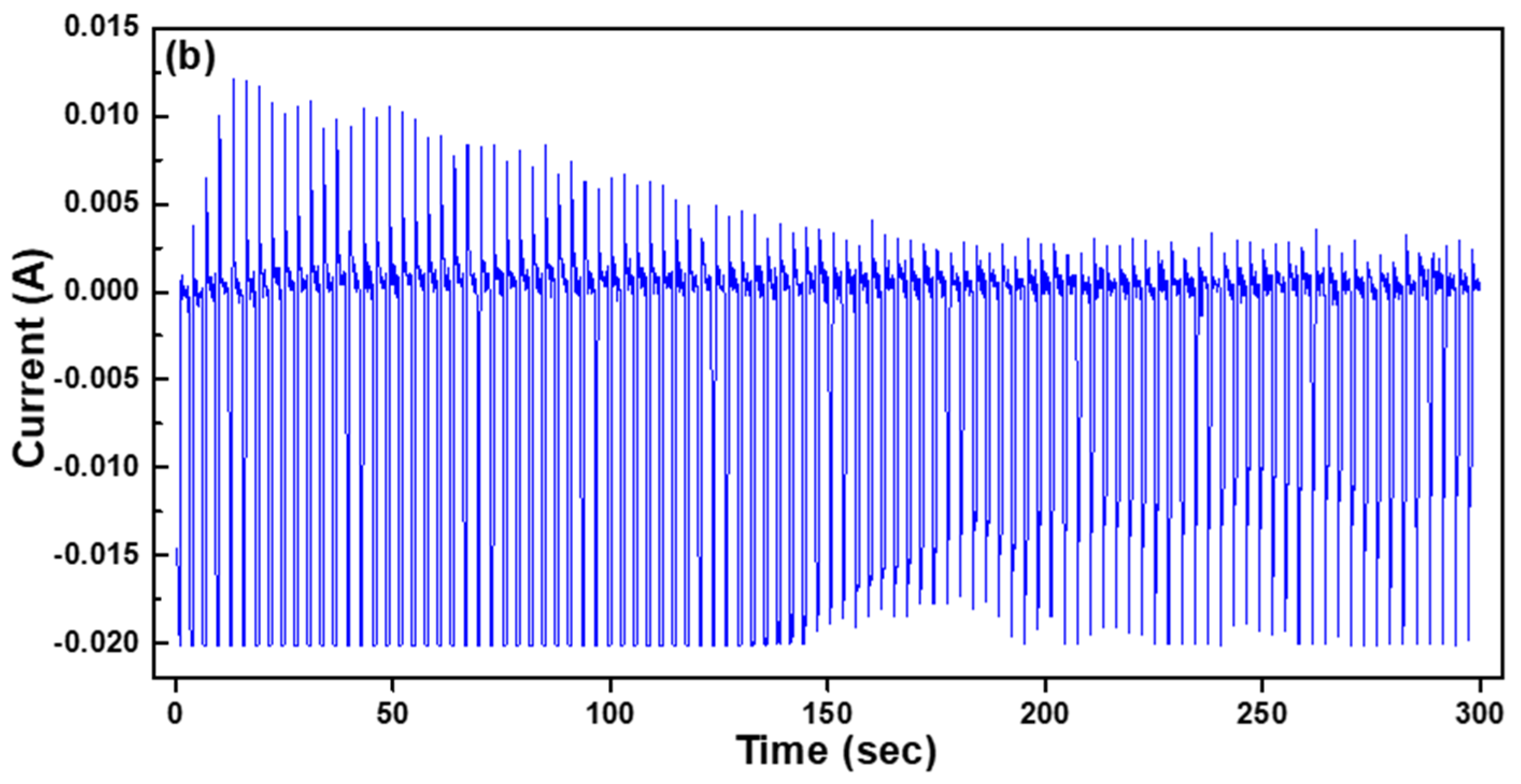
Figure 2a shows the variations of current and voltage during the first cycle and
Figure 2b shows the variation of current during the whole deposition process (0~300 s), respectively. They show that the deposition process was a pulsed electrodeposition with a duty cycle of 33%.
After the deposition process, the CIS films and CIS-NRs in the AAO templates were annealed at 250 °C for 15 min and then annealed at 450 °C for 15 min. The annealing process enhanced the crystallization, and made the CuSe phase melt and react with the CuInSe2 to obtain the CuInSe2 with a chemical dose close to 1:1:2, that is, the preferred crystal phase. The AAO template was removed using 0.6M phosphoric acid solution at 30 °C for 2 h. Finally, the KCN solution was used to etch the disk-typed Cu-rich or In-rich films, which were residual on the surfaces of the CIS-NRs. The Pt electrode was deposited using the direct current (DC) sputter in a pure Ar atmosphere. The ITO electrode was deposited using the DC sputter and the deposition parameters were as follows: Ar flow rate of 30 sccm, O2 flow rate of 0.8 sccm, deposition power of 100W, deposition time of 60 min, and deposition temperature of 100 °C. The ITO electrode deposited at these parameters had a resistivity of 1.08 × 10⁻³ Ω·cm and an average transmittance ratio (400~700 nm) of 91.68%. The morphologies of CIS nanomaterials were measured using a field emission scanning electron microscopy (FESEM), while nano-scale analyses of CIS nanomaterials were performed using transmission electron microscope (TEM). The crystalline structures of CIS nanomaterials were identified using X-ray diffraction (XRD) patterns with Cu Kα radiation.
3. Results
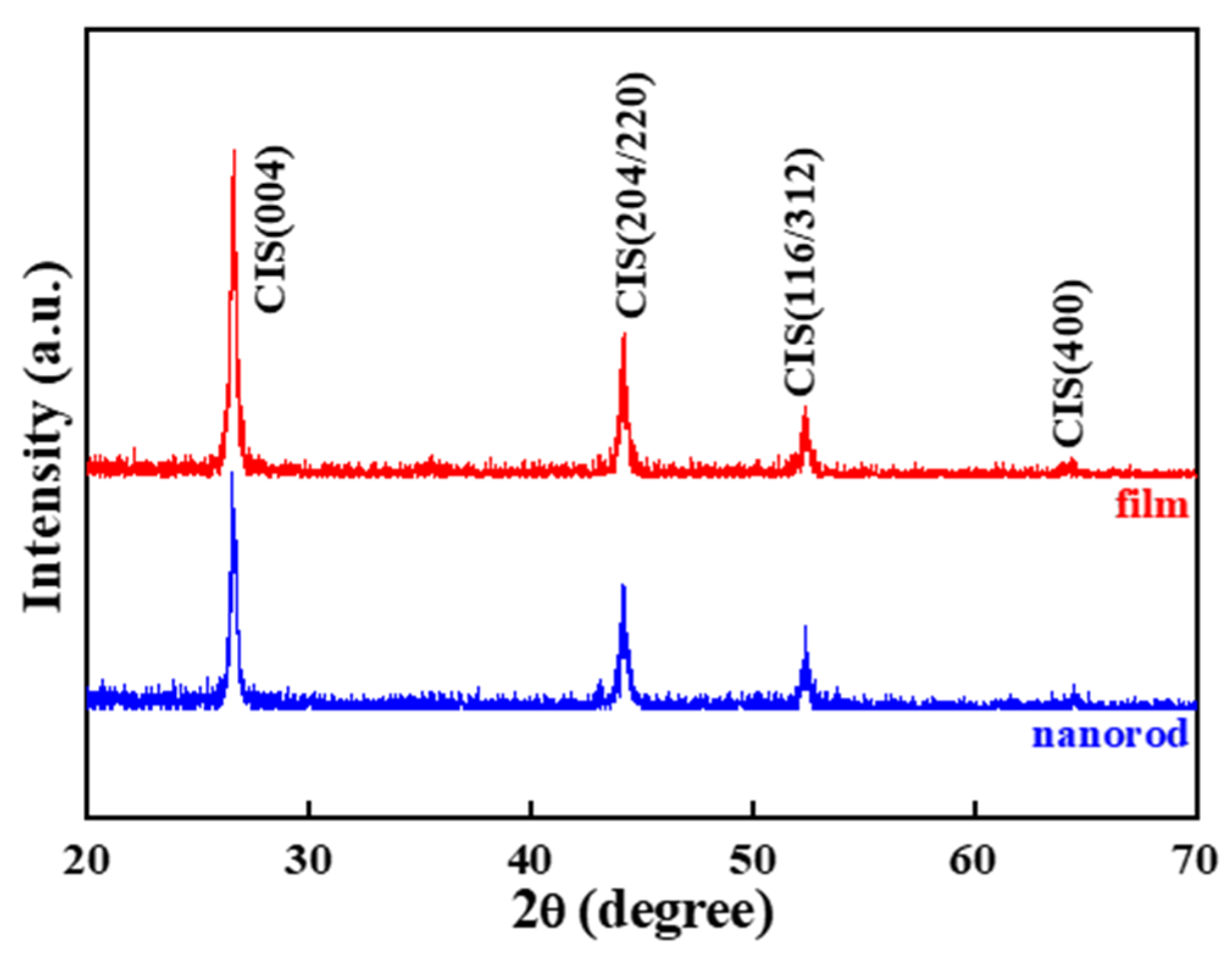
Figure 3 shows the diffraction characteristic peaks of the deposited CIS films and nanorods. Diffraction peaks at 2θ values of 26.61°, 44.20°, 52.32°, and 64.34°, which correspond to the diffraction planes of (112), (220/204), (312/116), and (400), were observed for the CIS phase. As the XRD pattern in
Figure 1 shows, the diffraction intensity of the CIS films was higher than that of the CIS-NRs. In addition, the full width at half maximum (FWHM) value of the (004) plane for the CIS films was smaller than that of the CIS-NRs. There are two reasons why the diffraction intensity of the CIS films was larger than that of the CIS-NRs. The first is that the crystallization of the CIS films is better than that of the CIS-NRs and the second is that the effective diffraction surface of the CIS films is larger than that of the CIS-NRs. Because the FWHM value of the CIS films is smaller than that of the CIS-NRs, we believe the better crystallization of the CIS films is the main reason for the difference in the diffraction intensities of CIS films and the CIS-NRs. However, both the deposited CIS films and the CIS-NRs have high crystallization for further applications of devices.
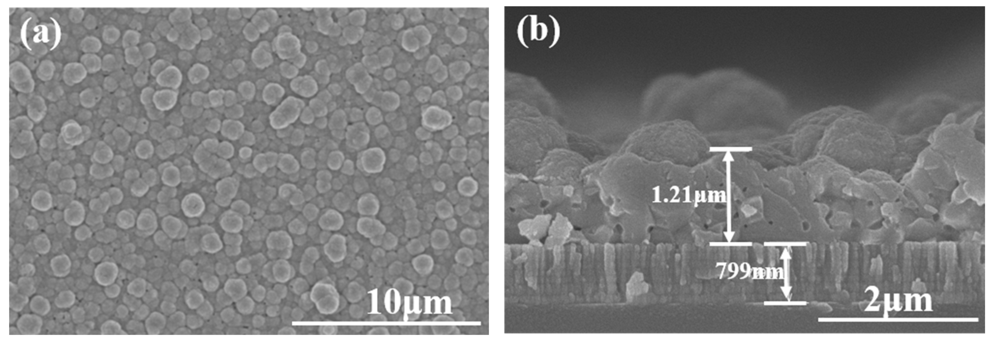
Figure 4 shows the SEM images of deposited CIS films on the surface of the Mo/Si
+ substrate.
Figure 4a shows that the CIS films had rough surfaces and a micro-crystalline structure and that the grain-size distributed from ~0.5 μm to ~1.6 μm.
Figure 4b shows that the thicknesses of the Mo electrode and CIS films were about 800 nm and 1.21 μm. In contrast,
Figure 4a shows the corresponding SEM images of deposited CIS films, and the elemental maps of CIS films were obtained by FESEM equipped with Energy Dispersive Spectrometer (EDX) for elemental Cu, In, and Se (not shown here). The elemental ratio of Cu:In:Se was about 27.90 (27.74~28.09):26.67 (26.51~26.88):45.43 (45.26~45.67), which was close to the ideal chemical ratio of 1:1:2. Because the Se/(Cu + In) ratio is smaller than 1 and the Cu/In ratio is larger than 1, the deposited CIS films had the properties of a p-type [
17]. The deposited film showed that it was richer in Cu than In, and it was the p-type CIS films.
A cross-sectional SEM image, a cross-sectional high-resolution transmission electron microscopy (HRTEM) image and TEM diffraction analysis of the CIS-NRs deposited on p
+-Si substrate are shown in
Figure 5. For the CIS-NRs, as
Figure 5a shows, the deposited nanorods expanded epitaxially on the p
+-Si substrate and their height was about 335 nm. The SEM analysis also found that the average particle size of the CIS-NRs was about 34.6 nm. The elemental maps of the CIS-NRs were also obtained by FESEM equipped with EDX for elemental Cu, In, and Se, and the elemental ratio of Cu:In:Se was about 28.17:21.21:50.62. Even the Se/(Cu + In) was larger than 1, but Cu/In was also larger than 1; therefore, the deposited CIS-NRs also revealed the properties of the p-type [
17]. To identify the microstructures, the HRTEM cross-sectional observation and nano-beam diffraction analyses were taken from the grown CIS-NRs, and the results are shown in
Figure 5b,c. From the HRTEM image in
Figure 4b, we found that the lattice spacing and lattice constant were 0.334 and 0.578 nm, respectively. The lattice parameters of deposited CIS-NRs calculated from the XRD patterns were
a = 0.5808 ± 0.0003 nm and
c = 1.159 ± 0.004 nm, which was the strongest match with the lattice constant observed using HRTEM. The measured lattice spacing of the CIS-NRs stem was 0.334 nm, which was also the strongest match with the hexagonal bismuth crystal structure and conformed with CuInSe
2 chalcopyrite (112) d-spacing. From the TEM diffraction analyses in
Figure 5c, we also found that the lattice distance matched the preferred crystal phase of the (112) plane.
In the past, Capon et al. deposited CuInSe
2 films that were obtained by selenization of ternary CuInSe
2 nanocrystals and mixtures of binary nanocrystals such as Cu
2Se and In
2Se
3. They investigated the d-spacing as a function of selenization time by fitting the raw in situ XRD data of the (112) diffraction peak. They found that the XRD pattern of the CuInSe
2 films depicted a lattice spacing of ~0.335 nm that corresponded to the distance between the (112) planes, indicating a good orientation along the (112) plane [
18]. Rincon and Ramlrez used the vertical Bridgman method to prepare the CuInSe
2 crystal and they found that a single phase with a chalcopyrite structure was present in the CuInSe
2 crystal with lattice parameters of
a = 0.5873 nm and
c = 1.1583 nm [
19]. Mobarak et al. used two different methods to prepare the CuInSe
2 compound and they found that the mean values of the lattice constants of the crystal prepared by the Bridgman method were
a =0.57823 nm and
c = 1.16192 nm, whereas those of the crystal grown by the traveling heater method were
a =0.5787 nm and
c =1.1574 nm, respectively [
20]. These results show that our prepared CIS samples have the good crystallinity with a chalcopyrite structure and a good orientation along the (112) plane.
The Schottky diode, which is also referred to as the Schottky barrier diode or hot-carrier diode, is a hetero-junction semiconductor diode formed by the contact of a semiconductor with a metal. For a typical Schottky diode, the used metal will act as the anode and the n-type semiconductor will act as the cathode, which means the current can flow from the metal side to the semiconductor side, but it cannot flow in the opposite direction. The different combinations of the metals and semiconductors can affect the forward voltage of the constructed diodes, and both n- and p-type semiconductors can develop as the Schottky barriers. However, the p-type typically can be used to fabricate a Schottky diode with a much lower forward voltage.
In this study, the work function of Al (Φ
Al) is about 4.28 eV and that of p
+-Si (Φ
p+-Si) is in the range of 4.61~5.17eV. From the theorem in
Figure 6, the Al/p
+-Si contact should be the Schottky contact. However, before the electrodeposition process, we first annealed the Al/p
+-Si contact at a high temperature, then Al was diffused onto the surface of the p
+-Si wafer. This process caused an increase in the doping concentration of the contact interface and reduced the width of the depletion region. This resulted in the electrons and holes tunneling the junction barrier and then the ohmic contact formed. The typical dark current–voltage (J-V) characteristic of the Pt/CIS-NRs/p
+-Si hetero-junction device is displayed in the
Figure 6, where
Figure 6a,b shows the normal scale and the log scale, respectively. The work function of CIS (Φ
CIS) is about 5.1 eV and that of Pt (Φ
Pt) is 5.65eV. From the theorem in
Figure 6, the CIS/Pt contact should be the ohmic contact. The J-V curves of the Pt/CIS-NRs/p
+-Si device in normal scale (
Figure 6a) and log scale (
Figure 6b) show that the CuInSe/p
+-Si produced symmetrical results, which show that all the interfaces of the Pt/CIS-NRs/p
+-Si device had ohmic contact.
The J-V curves of the ITO/CIS-NRs/p
+-Si device are shown in
Figure 7a,b for the normal scale and the log scale, respectively, which shows that the J-V curves were not symmetrical. When +1 V and −1 V were used as the standard to measure the current densities, the forward and reverse current densities were 0.35 mA/cm
a and −0.165 mA/cm
2, respectively, and the on/off ratio was 2.12. These results suggest that the interface of the ITO/CIS-NRs is a Schottky contact and the ITO/CIS-NRs/p
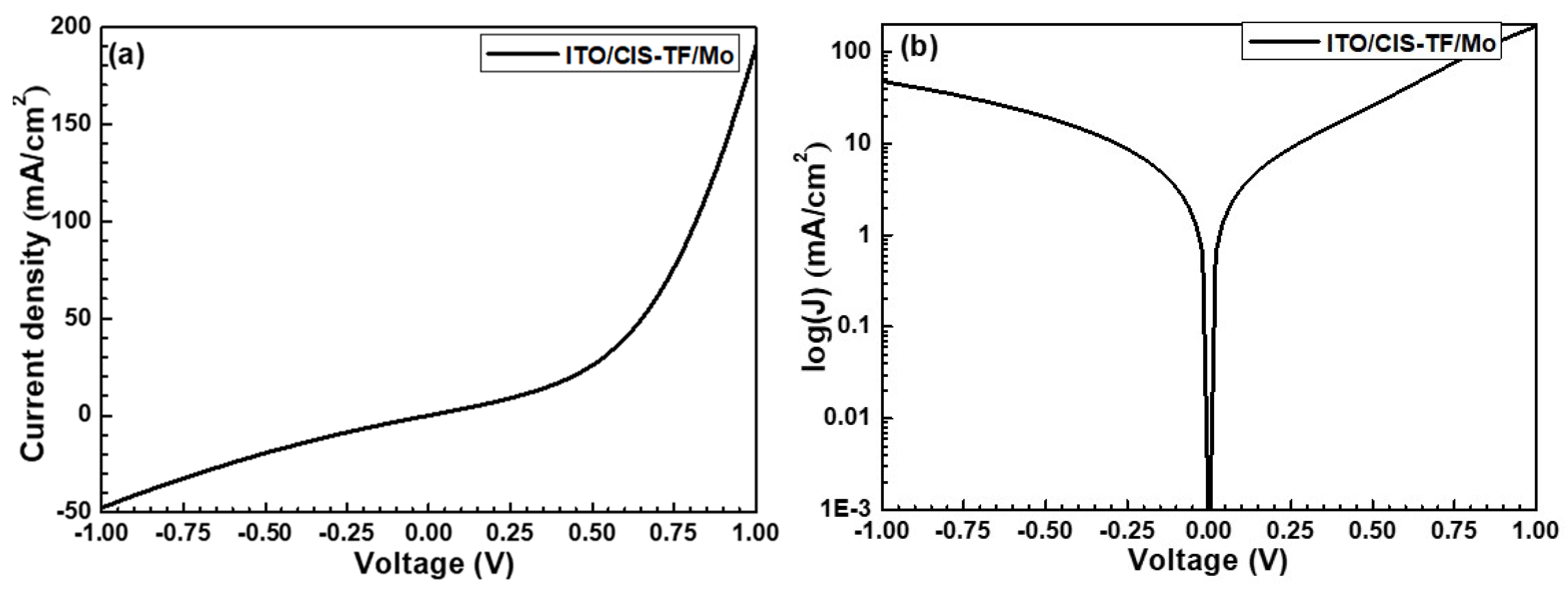
+-Si device can act as a Schottky diode. For the ITO/CIS-TF/Mo device, when +1V and -1V were used as the standard to measure the current densities, the forward and reverse current densities were 189.3 mA/cm
2 and −47.51 mA/cm
2, respectively.
Figure 8a,b shows the normal scale and the log scale, respectively, and the on/off ratio for these scales was 3.98. These results also suggest that the interface of ITO/CIS-TF is a Schottky contact.
For the ITO/CIS-TF/Mo device, its current densities of forward bias and reverse bias were higher than those of the ITO/CIS-NRs/p
+-Si device, and there are two possible reasons for these results. First, the contact interface of ITO/CIS-TF was larger and had better contact than that of the ITO/CIS-NRs device, and second, the contact interface of the CIS-TF/Mo was larger and had better contact than that of the CIS-NRs/p
+-Si device. The interfaces between the CIS-NRs/p
+-Si and CIS-TF/Mo were caused by the ohmic contact, therefore the Schottky effect was caused by the contact of the ITO/CIS-NRs and the ITO/CIS-TF. So far, the work function of ITO is not exactly defined. Chkoda et al. used photoelectron spectroscopy to measure the work function of commercial ITO, and their measured values were dependent on the cleaning air of substrates. When the glass substrate was cleaned by organic solvents, the Φ
ITO was 3.9–4.2 ± 0.1 eV and when the glass substrate was cleaned by Ar
+ sputtering, the Φ
ITO was 4.3 ± 0.1 eV [
21]. Beerbom et al. used photoemission spectroscopy and an ultra-high vacuum Kelvin probe to measure the work function of commercial ITO films on glass substrates, and their measured Φ
ITO values were in the range of 3.85~4.56 [
22]. Because the Φ
ITO value was smaller than the Φ
CIS value, there is no doubt that the Schottky effect was caused by the contact of the ITO/CIS-NRs and the ITO/CIS-TF.
Finally, Ag was used as the electrode to form the Ag/CIS-NRs/p
+-Si structure, and its J-V characteristic was also measured. The Φ
Ag was 4.26eV, which was smaller than the Φ
CIS value and the Ag/CIS-NRs/p
+-Si device formed the Schottky diode.
Figure 9a,b shows the normal scale and log scale, respectively. For the Ag/CIS-NRs/p
+-Si device, when +1 V and −1 V were used as the standard to measure the current densities, the forward and reverse current densities were 0.48 mA/cm
2, −0.06 mA/cm
2, respectively, and the on/off ratio was 8.07. These results show that interface of the Ag/CIS-NRs was a Schottky contact and the Ag/CIS-NRs/p
+-Si device acted as a Schottky diode.
In this study, the Ag/CIS-NRs/p
+-Si diode had the larger on/off ratio, therefore its C-V characteristic was also measured and the results are shown in
Figure 10a, and the relationship for 1/C
2-V is shown in
Figure 10b. The 1/
C2 can be used to find the built voltage (
Vbi) of the Ag/CIS-NRs/p
+-Si diode, and the Equation for the relationship between 1/
C2 and
Vbi is shown in Equation (1). Because the slope shown in
Figure 10b is positive, this shows that the CIS-NRs is a p-type semiconductor. From the extrapolation line of the slope, the
Vbi can be found at the intercept of the slope and voltage axis, and
Vbi is 0.22 V. The parameter
was used to measure
and was obtained from [
23], where
=
= 8.85 × 10
−14 × 13.5
F/cm = 1.19475 × 10
−12 F/cm and
Nv = 1.5 × 10
19 cm
−3. The relationships to find the Schottky barrier (Φ
SH) and the carrier concentration (
NA) of the CIS-NRs can be expressed in Equations (2) and (3). When we brought
= 0.22V into Equations (2) and (3), the calculated Φ
SH value was 0.7 V and the calculated
NA value was 1.38 × 10
11 cm
−3.
Because the Ag/CIS-NRs/p
+-Si diode has the maximum on/off ratio of 8.07, we used its properties to compare the performance of the Schottky diodes with those fabricated with other techniques. Tecimer et al. used a thermal evaporation method to synthesize CuInSe
2 films on a Mo-coated glass substrate, and the carrier concentration of the deposited CuInSe
2 films was 4.0 × 10
17 cm
−3. After the CuInSe
2 films were deposited, Al metal was evaporated on the upper surface of the CuInSe
2 films as a front contact to form the Al/CuInSe
2/Mo Schottky diode [
24]. The forward and reverse current densities of the Al/CuInSe
2/Mo Schottky diode (measured at 300 K and at +1 V and −1 V) were ~0.42 mA/cm
2 and ~−0.07 mA/cm
2, the on/off ratio was ~6, and the Φ
SH value was 0.729 V. Hamrouni et al. electrodeposited the CuInSe
2 films on FTO substrates and annealed them at 400 °C in a vacuum for a duration of 20 min, and the carrier concentration of deposited CuInSe
2 films at 300 K was 8.66 × 10
15 cm
−3. Additionally, Al metal was evaporated on the upper surface of the CuInSe
2 film as a front contact to form the Al/p-CuInSe
2/Mo Schottky diode [
16]. The forward and reverse current densities of the Al/CuInSe
2/Mo Schottky diode (at 300 K) were 0.151 mA/cm
2 and −0.038 mA/cm
2, respectively, the on/off ratio was 3.98, and the Φ
SH value was ~1.22 V. As compared with the two Al/p-CuInSe
2/Mo Schottky diodes, even our deposited CIS films had the lower value of carrier concentration (N
A), and our investigated Ag/CIS-NRs/p
+-Si diode had the larger forward current density of 0.48 mA/cm
2 and an on/off ratio of 8.07.


